Acoustoelectric effects in very high-mobility -SiGe/Ge/SiGe heterostructure
Abstract
Measurement results of the acoustoelectric effects (surface acoustic waves (SAW) attenuation and velocity) in a high-mobility -SiGe/Ge/SiGe structure are presented. The structure was LEPECVD grown with a two dimensional (2D) channel buried in the strained Ge layer. The measurements were performed as a function of temperature (1.5 - 4.2 K) and magnetic field (up to 8.4 T) at different SAW intensities at frequencies 28 and 87 MHz. Shubnikov-de Haas-like oscillations of both SAW attenuation and the velocity change have been observed. Hole density and mobility, effective mass, quantum and transport relaxation times, as well as the Dingle temperature were measured with a method free of electric contacts. The effect of heating of the 2D hole gas by the electric field of the SAW was investigated. Energy relaxation time and the deformation potential constant determined.
pacs:
73.63.Hs, 73.50.Rb, 72.20.Ee, 85.50.-nI Introduction
Two-dimensional semiconductor systems are usually a multilayer structure with a 2-dimensional conducting layer in the depth of the order of hundreds of angstrom from the surface. Determination the key parameters of these structures, involves customarily the measurement of transport properties such as resistance, magnetoresistance, the Hall effect on a direct current. Measurements of these effects require ohmic electrical contacts. The fabrication of such contacts often requires the heating of the studied samples, which can lead to irreversible changes of their properties. Besides it requires a Hall bar to be configured to meet the geometrical conditions for the correct measurement of effects. Hall bridge manufacturing usually requires a high technology photolithography. Moreover, the absence of contacts eliminates otherwise possible carrier injection into the low-dimension interface from the contact areas.
The present paper provides main heavy hole characteristics in a high-mobility -SiGe/Ge/SiGe heterostructure. The results were obtained with an acoustic method which is deprived of the disadvantages mentioned above as it implies use of samples of rectangular shape and the complete absence of electrical contacts.
II Experimental results
Object
The system under study was the sample -SiGe/Ge/SiGe (K6016) investigated earlier on a direct current in Ref. kanel, . The sample structure is illustrated on Fig. 1(a).
In the system under study the 2D-channel is in strained Ge. The threefold degenerated valence band of Ge is split due to a strain into 3 subbands, top of which is occupied by heavy holes.
The entire structure was grown by low-energy plasma-enhanced chemical vapor deposition (LEPECVD), by making use of the large dynamic range of growth rates offered by that technique kanel, . The buffer, graded at a rate of about 10m to a final Ge content of 70, and the 4 m thick constant composition layer were grown at a high rate of 5-10 nm/s while gradually lowering the substrate temperature from 720C to 450C. The active layer structure, consisting of a pure 20 nm thick Ge layer sandwiched between cladding layers with a Ge content of about 60 and a Si cap, was grown at a low rate of about 0.3 nm/s at = 450C. Modulation doping was achieved by introducing dilute diborane pulses into the cladding layer above the channel after an undoped spacer layer of about 30 nm.
Method
The experimental setup is illustrated in Fig. 1(b). It includes a piezoelectric crystal (LiNbO3), where a surface acoustic wave (SAW) is excited at its surface by inter-digital transducers. A SAW propagating along the surface of lithium niobate is accompanied by high-frequency electric field. This electric field penetrates into a 2DHG located in a semiconductor heterostructure mounted on the surface. The field produces electrical currents which, in turn, cause Joule losses. As a result, there are electron-induced contributions both to the SAW attenuation and to its velocity. These effects are governed by the complex high-frequency conductivity, .
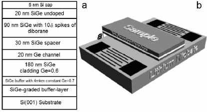
This ”sandwich”-like experimental configuration allows to carry out contactless acoustoelectric experiments on non-piezoelectric 2D systems, for example, on SiGe/Ge/SiGe.
In the present experiment the acoustoelectric effects - attenuation and the SAW velocity change - have been measured at frequencies 28 and 87 MHz and a magnetic field up to 8.4 T in a temperature range 1.6 - 4.2 K.
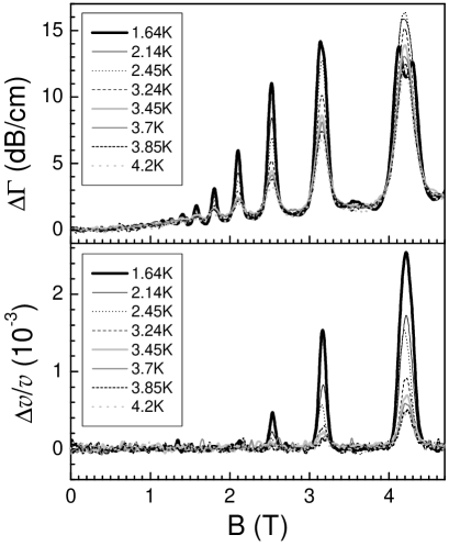
Fig.2 shows the magnetic field (B) dependences of the attenuation and the SAW velocity change in the K6016 sample.
One can see that in magnetic field the absorption coefficient and the velocity change both undergo Shubnikov-de Haas (SdH) type oscillations, analogous to that in on a direct current.
From the measured values of and both the real, and imaginary, parts of the high-frequency (AC) conductivity could be obtained with the aid of equations (II,II). Since , [ildPRB, ]:
| (1) | |||
| (2) |
where is the electro-mechanic coupling constant for lithium niobate (Y-cut), and are the SAW wave vector and velocity in LiNbO3, respectively. is the gap between the piezoelectric plate and the sample, distance between the sample surface and the 2DHG layer; , and are the dielectric constants of LiNbO3, of vacuum, and of the semiconductor, respectively; and are complex functions of , , , and . In order to obtain and from equations (II,II) one should know the values of and . 1.45 cm is determined in the technological process of the sample production, and is determined by fitting the experimental data at those magnetic fields where the conductance is metallic and essentially frequency independent. The value of depends on the assembling quality of the sample-LiNbO3 sandwich, and was in this experiment cm. AC conductivity components and as a function of magnetic field were measured at different temperatures.
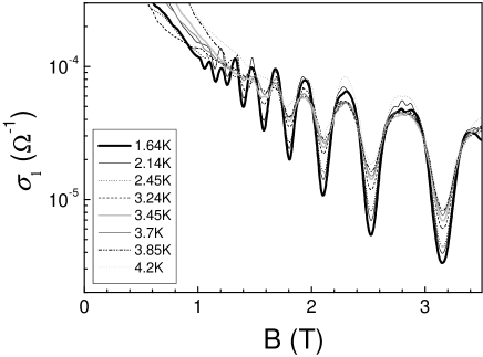
Fig. 3 illustrates the magnetic field dependence of the real component of the complex high-frequency conductivity, obtained from SAW measurements at different temperatures using Eqs. (II,II).
Determination of parameters
1) The density of holes, obtained from the SdH oscillations minima appeared to be: cm-2
2) Mobility temperature dependence at =0.
According to Ando’s theory [ando, ], in a magnetic field can be expressed in a form:
| (3) |
where is the classical Drude conductivity, is the zero magnetic field conductivity, is the cyclotron frequency, is the transport relaxation time; , where is the mobility, =3cm/s.
All acoustic method measurements are relative, thus it is impossible to obtain from them directly the absolute values of either conductivity, or mobility at =0. However, in case of high mobility samples, where there are many SdH oscillations in the relatively low magnetic field region (no localization) these values could be determined. In this case one could plot - mean value between the oscillations envelope, as a function of . The mobility at =0 is determined from the slope of this line.
| (4) |
Fig. 4 presents the mobility value, obtained with the method described as a function of temperature.

The value can be determined with the aid of the density and mobility, obtained in our measurements. For =1.7 K and =0 =0.008 Ohm-1 which value by only 5 differs from =0.0076 Ohm-1 measured in Ref. kanel, .
3) Determination of the effective mass and of the ratio , where is the quantum relaxation time.
| (5) |
where is the Fermi energy.
The effective mass is conventionally determined from the temperature dependences of the oscillation amplitude at different magnetic fields in the 1.5 - 2.1 T range. The ratio obtains from the oscillation amplitude dependence on at different temperatures. As a result, one has , =4.90.2. According to Ref. gold, , this corresponds to the holes scattering at the charged impurity centers with the screening taken into account. The values of , , and thus obtained are very close to those of Ref. kanel, .
Absolute values at -1.7 K are: the transport relaxation time s, the quantum relaxation time s and the Dingle temperature =1.24 K.
4) Energy relaxation time .
Additional measurements of the acousto-electronic effects dependence on the SAW power at 1.6 K in a magnetic field up to 2.5 T were performed for the determination of the relaxation time of energy .
Fig. 5 depicts the attenuation, , dependence on magnetic field for diverse SAW powers at the source generator output.
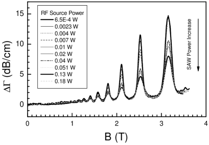
As it is easily seen in Fig. 5, depends on the SAW power introduced into a sample. Since all holes parameters obtained above were measured in their delocalized state, it seems natural to suppose that in the same magnetic field region the cause of dependence on SAW power is the 2DHG heating in strong electric field of the SAW. Following Ref. HeatSAW, , we shall use the concept of the hole gas temperature and determine it comparing two dependences: and , where is the RF source power, is the lattice temperature. This comparison enables one to establish correspondence between the hole gas temperature and the RF source output power. The energy loss rate, , dependence on the hole gas temperature was plotted for the determination of the relaxation mechanism.
According to Ref. HeatSAW, , the energy losses rate
| (6) |
where is the electric field produced by the SAW and penetrating the channel with the 2D holes, is the attenuation and is the SAW power at the sample entrance. is determined as the output power of the RF source generator minus the loss associated with the electro-acoustic conversion and transmission line.

relation seems the most suitable for experimental data interpretation. Here could be determined from the slope of the . The dependence of this kind evidences that the energy relaxation is determined by the unscreened acoustic phonon deformation potential scattering. At the limit of weak heating, when , the energetic relaxation time could be estimated, following Ref. HeatSAW, :
| (7) |
In our case, when =5, one gets: =10-10 s.
Regarding the energy relaxation as a deformation potential scattering with a weak screening, one can determine the deformation potential value. Indeed, according to Ref. Karpus, , the energetic loss value could then be evaluated with the aid of a formula:
| (8) |
where and are the longitudinal sound velocity and the density of Ge, is the wavevector of the electron with an energy of Fermi (), (x) is the Rihman function, is the deformation potential. =(121) eV.
Deformation potential of unstressed Ge, determined in Ref. deform, , =(16.20.4) eV.
As a conclusion, in Fig. 7 presented are the magnetic field dependence of both DC conductivity from [kanel, ], and that of the real part, , of the AC conductivity at = 1.7 K.
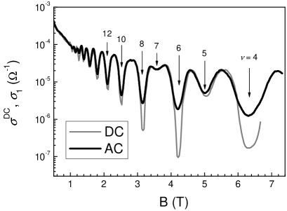
was obtained from Fig.3 of Ref. kanel, as .
As one can conclude observing the figure, the curves at = 1.7 K practically coincide up to =2.1 T, and then exceeds and the difference between these values grows with the growth of the magnetic field. In relatively week magnetic field the carriers are delocalized = and =0 [loc, ], the conductivity mechanisms for DC and AC are the same. With the increase of the magnetic field the holes in the SdH oscillation minima became localized, and the conductivity turns to be hopping. DC hopping differs from hopping in AC. In the DC case hopping is accomplished to the nearest neighbour with a constant activation energy, than changing to the variable length hopping (see [Greenbook, ]). In the alternating electric field the hopping conductivity is treated with the ”two site model”, in this case always [ildPRB, ; Pollak, ; Efros, ]. As soon as the 2DHG parameters should be determined when the carriers are not localized, the curve of Fig. 7 informs that it could be done at magnetic fields, not exceeding 2.1 T.
III Conclusion
In conclusion we draw here a comparative table with data obtained via conventional dc measurements [kanel, ] and using contactless SAW technique.
| DC | AC | |
|---|---|---|
| (cm-2) | ||
| (cm2/Vs) | ||
| 7.5 | 4.90.2 | |
| (s) | - | (6.30.1)10-10 |
| (eV) | - | 121 |
Acknowledgements.
This work was supported by grants of RFBR 08-02-00852; the Presidium of the Russian Academy of Science, the Program of Branch of Physical Sciences of RAS ”Spintronika”.References
- (1) H. von Känel, M. Kummer, G. Isella, E. Müller, T. Hackbarth, Appl. Phys. Lett. 80, 2922 (2002).
- (2) I.L. Drichko, A.M. Diakonov, I.Yu. Smirnov, Y.M. Galperin, and A.I. Toropov, Phys. Rev. B62, 7470 (2000).
- (3) T. Ando, Y.Uemura, J. Phys. Soc. Japan. 36, 959 (1974).
- (4) A.Gold, Phys. Rev. B38, 10798 (1988).
- (5) I.L. Drichko, A.M. Diakonov, V.D. Kagan, A.M. Kreshchuk, T.A. Polyanskaya, I.G. Savel’ev, I.Yu. Smirnov and A.V. Suslov, Fiz. Tekh. Poluprov. 31, 1357 (1997) [Semiconductors 31, 1170 (1997)].
- (6) V. Karpus, Fiz. Tekh. Poluprov. 22, 439 (1988) [Sov. Phys. Semicond. 22, 268 (1988)].
- (7) I. Balslev, Phys. Rev. 143, 636 (1966).
- (8) I.L. Drichko, A.M. D’yakonov, A.M. Kreshchuk, T.A. Polyanskaya, I.G. Savel’ev, I.Yu. Smirnov and A.V. Suslov, Fiz. Tekh. Poluprov. 31 451 (1997) [Semiconductors 31 384 (1997)].
- (9) B.I. Shklovskii and A.L. Efros, Electronic properties of doped semiconductors, 1984, pp. 388, Springer-Verlag (Berlin, New York).
- (10) M. Pollak, T.H. Geballe, Phys. Rev. 122, 1742 (1961).
- (11) A.L. Efros, Zh. Eksp. Teor. Fiz. 89, 1834 (1985) [JETP 89, 1057 (1985)].