In situ observation of stress relaxation in epitaxial graphene: Supplement I/II
1 Parallel and rotated graphene phases in LEEM and PEEM

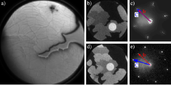
We observe two domains of graphene on Ir(111). In 1 a) a bright field LEEM image is shown. Graphene in the upper area is imaged brighter than graphene in the lower area, and there is a gulf of bare iridium cutting in from the right. The images b) and e) are photo emission electron microscopy (PEEM) images of the same region. Iridium is imaged black, graphene from the upper area of a) is imaged darker than graphene from the lower area. The bright circle displays the position of the electron beam for the LEED images in c) and e). The LEED patterns show that in the case of bright graphene in LEEM (dark in PEEM), there is a rotation of graphene’s direction with respect to the substrate’s direction whereas in the dominating phase - darker in LEEM (bright in PEEM) the dense packed directions of graphene and Ir(111) are parallel.
2 Delamination around heptagon-pentagon pairs

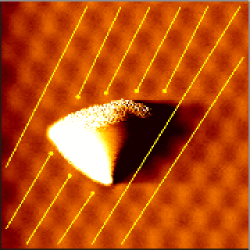
The STM topograph in 2 shows a bulge in the graphene layer. The extra ending line of moiré maxima (three on one side of the protrusion, but four on the other) indicate an extra row of atoms terminating in a pair of heptagon-pentagon carbon rings [1]. We speculate that the bulge is a nucleus of a wrinkle originating from such a point defect.
References
- [1] J. Coraux, A. T. N’Diaye, C. Busse, and T. Michely. Structural coherency of graphene on Ir(111). Nano Lett., 8:565–570, 2008.