Current-voltage characteristics of tunable ferromagnet-silicon-ferromagnet channels in the spin blockade regime
Abstract
The steady current-voltage characteristics of ferromagnet-silicon-ferromagnet channels with tunable emitter and collector polarizations are investigated in the presence of spin blockade generalizing the model developed by Pershin Yu V and Di Ventra M (2008 Phys. Rev. B 77 073301). The dependence of the critical current on both collector and emitter polarizations is obtained analytically. It is found that the current amplitude in the channel can be effectively tuned by varying the difference between the collector and emitter ferromagnet polarizations which allows to perform the magnetic manipulation of the electrical current in wide class of both n- and p-doped, low- and high-Ohmic semiconductor channels coupled to ferromagnetic leads.
pacs:
72.25.Dc, 72.25.Mk, 73.23.Hk1 Introduction
The progress of spintronics and physics of heterostructures which can be observed during the last years [1, 2] is focused on various physical phenomena, and one of them which attracts a considerable attention is the spin-dependent transport through semiconductor/spin-polarized junctions [3, 4, 5, 6, 7, 8, 9, 10, 11, 12, 13, 14, 15]. The physics of carrier polarization and its influence on transport in composite structures such as semiconductor/ferromagnet has been studied both theoretically [4, 6, 7, 8, 9, 12, 13, 14, 15] and experimentally [3, 5, 10, 11]. One of the models describing the spin-resolved carrier concentrations and currents at the junction is the two-component drift-diffusion model [6, 13, 14] which predicted highly nonlinear and saturating current-voltage dependence at a single semiconductor/feromagnet junction due to the effect of spin blockade [13, 14]. In this model the detailed structure of the charge and current distribution at the junction area [4, 6] as well as the Schottky barriers [7, 8], the charge redistribution effects [9], and the bound states [12] are not taken into consideration. Still, the qualitative and distinguishable behaviour of current saturation due to the effect of spin blockade is reliably predicted under various system parameters such as the junction/semiconductor resistance ratio. The spin blockade regime arises from the spatial distribution of the spin-minority carriers which cannot enter the ferromagnet region and form a cloud near the junction which growth prevents the further increase of spin-majority carrier transport if the current exceeds a threshold value called the critical current. Further studies have shown the importance and promising applications of this effect also for non-stationary phenomena such as spin memory effects [15]. The models described above were applied mainly to GaAs-based semiconductor channels, but is is known that the silicon-based structures are also of big interest for spintronics due to the dominating place of silicon in currently available electronic technologies. More, the technologies of fabricating the silicon/ferromagnet structures such as Si/Si:Mn formed on a basis of diluted magnetic semiconductors have been intensively developed during the last few years [16, 17] which makes their future applications in spintronics promising and creates certain questions about the phenomena described above. Is there a spin blockade regime in a silicon/ferromagnet junction at specific values of applied voltage, carrier mobility and concentration ? If so, what is the critical current density and how it depends on the silicon and ferromagnet parameters such as the carrier polarization in ferromagnets and the conductivity of the semiconductor channel? How deep can we modulate the current in the channel by manipulating the polarization of emitter or collector ferromagnets relative to each other? In the present manuscript we study these problems in the framework of a simple but effective model of transport in the spin blockade regime [13, 14] which we generalize for the case of arbitrary carrier polarizations in the emitting and collecting ferromagnetic regions of the channel as well as for wide range of low- and high-Ohmic n-doped and p-doped silicon samples. It is found that the current can be deeply modulated by changing the spin alignment in the emitter and/or collector ferromagnet since the critical current density is very sensitive to it. We find the analytical expression for the critical current density and calculate the current-voltage dependencies for various combinations of the channel/contact resistance ratios, as well as for n- and p-type of doping with both high and low concentrations. The manuscript is organized as follows: in Section 2 we derive a model generalizing the description of the spin blockade regime for the two-ferromagnet channel with arbitrary polarizations in the emitter and collector ferromagnets and discuss the properties of the critical current density, in Section 3 we plot and discuss the current-voltage characteristics for various combinations of system parameters, and the conclusions are given in Section 4.
2 The model
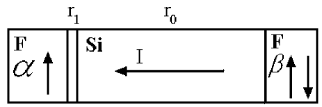
The schematic view of the ferromagnet-silicon-ferromagnet channel is shown in Figure 1. The collector ferromagnet with the junction resistance is separated from the emitter ferromagnet by a bulk silicon channel with length which we consider as exceeding the spin diffusion length given by [6, 13, 14]
| (1) |
where and are the carrier diffusion coefficient and drift mobility, respectively, is the electric field inside the channel, and ns is the typical spin relaxation time [2]. One can see from (1) that is maximal at zero electric field when and when the diffusion coefficient and spin relaxation time are big, or, since is coupled to the mobility via the Einstein relation [18], it is clear that the spin diffusion length grows with the mobility. Since the mobility in the bulk silicon is typically lower than the one for GaAs [19], for the given parameters of the silicon the condition is already fulfilled if mkm which is a reasonable channel length of bulk semiconductor structures. Hence, from the point view where the spin-resolved concentration decay length is considered, the distance between emitter and collector ferromagnets here can be taken as infinite which simplifies the boundary conditions. The key parameters of our model are the variable polarization degrees and in the collector and emitter ferromagnets describing the state of their non-ideality as well as the chosen direction of polarization for the majority of carriers. For example, the pair , corresponds to the previously investigated case [14] where the carriers are fully polarized in the collector and fully unpolarized in the emitter. Correspondingly, the choice , describes the situation when the collector and emitter are highly polarized in the same direction while the values , describe the opposite polarization at the emitter. We adopt the labeling for the spin-resolved current with spins in ferromagnets aligned up (down). If is the total current density, than the spin-resolved current at the collector which means that corresponds to an ideal ferromagnet where magnetic moments are all aligned up (down), and describes the unpolarized current. The same labeling is adopted for the carrier polarization generated by the emitter ferromagnet with polarization . The main purpose of the present paper is to find out how deep is the influence of the various and differences reflecting the polarization switch on the total electrical current in the channel. We include in our model the channel and contact zero-bias resistances and (see Figure 1) with variable ratio, and the direction of the carrier motion is labeled as (for the electrons the actual current is ). The spin blockade may occur in the contact region at the collector (left F in Figure 1) if the polarizations and significantly differ from each other, which enhances the contact resistance from the zero-bias value as long as the current builds up.
The model for the spin-resolved current densities and spin-resolved concentrations where is the total carrier concentration is well-known [6, 13, 14] and consists of the continuity equation
| (2) |
and the equation for the spin-resolved current
| (3) |
These equations should be accompanied by the boundary conditions at the collector contact and at the other boundary of the channel which is in our problem can be considered as . In this case the steady-state solution of (2) exists [13, 14] which has the form of two exponents decaying to their concentrations defined by the boundary conditions at the emitter. In our model the emitter ferromagnet is described by the arbitrary polarization which generalizes the unpolarized case considered previously [13, 14], so
| (4) | |||
| (5) |
The steady-state solution of (2) satisfying the boundary condition (5) at the emitter and the normalizing condition has the form
| (6) | |||
| (7) |
where is the inverse decay length defined in (1). The parameter should be determined from the boundary condition at the collector when . If the collector is a non-ideal ferromagnet with the polarization , then the spin-resolved current at the collector
| (8) |
and the other boundary condition at the emitter is satisfied automatically. The total current density is related to the electric field in the channel via usual relation which allows to construct a closed equation for the current density and applied voltage. From (8) it follows that the conductivity of the collector junction is proportional to the concentration of the majority carriers, and at the absence of the current the junction resistance has a predetermined value while the silicon channel with length and cross-section is described by the resistance defined in a usual way by the carrier mobility, concentration and geometric dimensions as . After a simple algebra we obtain the Ohmic law which reads in our case similar to the one obtained previously [14] for a non-polarized emitter with ,
| (9) |
but in our generalized model the parameter defined as the critical current density [14] depends on both the collector and emitter ferromagnet polarizations and :
| (10) |
where
| (11) |
is the critical current density for the case of fully polarized collector ferromagnet with and fully unpolarized emitter with [14]. Indeed, for and the value of from (10) is equal to .
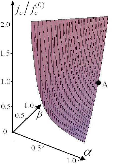
The main property of equation (9) determining the current-voltage characteristic is the current saturation occurring at current densities comparable to . Thus, it is of interest to investigate the critical current density (10) in more details with respect to the tunable polarization parameters and of the collector and emitter ferromagnets. In Figure 2 the three-dimensional plot is shown for the critical current density (10) measured in units of . The case of fully polarized carriers in the collector with and fully unpolarized electrons in the emitter considered in [14] is shown by a reference point A when . It is clear from (10) that diverges along the line which means that in the case of a perfect coincidence of the spin alignment in the emitter and collector the critical current can never be reached and there is no spin blockade in this limit. In the opposite limit of maximum difference between and the value of is considerably smaller than , so the spin blockade here occurs at lower current densities. The observed large variations of the critical current density are important for the desired high degree of control on the electrical current flowing through the ferromagnet-silicon-ferromagnet channel which can be achieved by variations of at least one ferromagnet polarization, say the emitter polarization . Below we shall see that these expectations are confirmed by the current-voltage dependencies in both n-doped and p-doped channels with both low- and high-Ohmic resistance.
3 Current-voltage characteristics
The current-voltage characteristics for n-doped and p-doped silicon channels with high and low carrier concentration are shown in Figures 3 and 4, respectively.
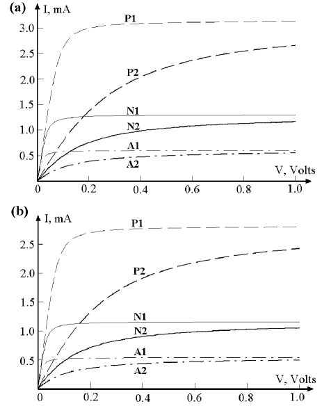
The data for the room temperature drift mobility of electrons and holes in the bulk silicon doped with various concentrations was taken from the standard reference plots [19], allowing to estimate both channel resistance for a bulk silicon sample with mkm and and the reference critical current density from (11). In Figure 3 the results are shown for the silicon channel with high carrier concentration where the reference critical current density is within the range of , and the channel resistance Ohm. On each plot the three families of curves correspond to three positions of the ”spin valve” emitter while the carriers at the collector are always highly polarized with . Each family has two curves labeled 1 and 2 (bold) which corresponds to the low and high ratios of the junction and channel resistances and . The solid curves N1, N2 describe the case of non-polarized carriers at the emitter with which was considered in [14], the dashed curves P1, P2 are for the emitter polarization which is close to the collector polarization , and the dash-dotted curves A1,A2 are for the emitter polarization which differs significantly from the one of the collector. For both type of carriers and for both low and high ratios of the contact/junction resistance ratio the current saturation is observed being the indication of the spin blockade regime. The switch between different emitter polarizations leads to strong modulations of the current saturation amplitude, creating the possibility of the magnetization control on the current.
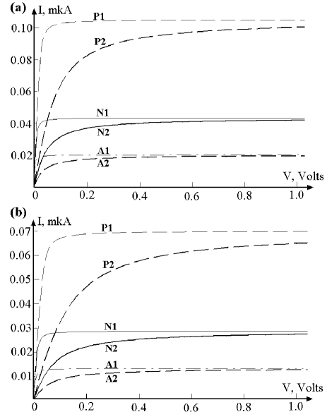
To compare the results for low-Ohmic samples with the high-Ohmic ones, we present in Figure 4 the current-voltage characteristics for the silicon channel doped with low carrier concentration where the reference critical current density is much lower and is within the range of . The channel resistance is correspondingly much higher, and we consider kOhm for n-doped and p-doped samples, respectively. The labeling of all curves is the same as in Figure 3, and the maximum achievable currents are much lower due to significantly smaller carrier concentration which decreases the conductivity. One can draw the same conclusions about the spin blockade manifestation and polarization control of the current amplitudes mentioned above which obviously can be applied also for the case of low carrier concentrations. We can conclude that the main goal of the present model which is the achievement of a deep current modulation by the magnetization switch at the emitter can be reached in both low- and highly-doped silicon samples, with both n-type and p-type doping and with both low and high ratios of the junction/channel resistances. Hence, the proposed model of the tunable current-voltage characteristics in a ferromagnet-silicon-ferromagnet channel seems to be applicable to a rather wide range of ferromagnet-semiconductor structures.
4 Conclusions
We have studied the steady-state current-voltage characteristics of ferromagnet-silicon-ferromagnet channels with long bulk silicon sample having the length exceeding the spin diffusion length. The current behaviour was investigated in the presence of spin blockade regime at the collector junction, and the dependence of the critical current on both collector and emitter polarizations has been obtained analytically. It was found that the current amplitude can be effectively tuned by varying the difference between the collector and emitter ferromagnet polarizations which allows to perform the magnetic manipulation on the electrical current in wide class of both n- and p-doped, low- and high-Ohmic semiconductor channels coupled to ferromagnetic leads.
References
- [1] Awschalom D D, Loss D and Samarth N (eds) 2002 Semiconductor Spintronics and Quantum Computation (Nanoscience and Technology) (Berlin: Springer)
- [2] Zǔtić I, Fabian J and Das Sarma S 2004 Rev. Mod. Phys. 76 323
- [3] Kawakami R K, Kato Y, Hanson M, Malajovich I, Stephens J M, Johnston-Halperin E, Salis G, Gossard A C and Awschalom D D 2001 Science 294 131
- [4] Zǔtić I, Fabian J and Das Sarma S 2002 Phys. Rev. Lett. 88 066603
- [5] Epstein R J, Malajovich I, Kawakami R K, Chye Y, Hanson M, Petroff P M, Gossard A C and Awschalom D D 2002 Phys. Rev. B 65 121202(R)
- [6] Yu Z G and Flatté 2002 Phys. Rev. B 66 201202(R)
- [7] Albrecht J D and Smith D L 2002 Phys. Rev. B 66 113303
- [8] Albrecht J D and Smith D L 2003 Phys. Rev. B 68 035340
- [9] Yu Yue, Li Jinbin and Chui S T 2003 Phys. Rev. B 67 193201
- [10] Stephens J, Berezovsky J, McGuire J P, Sham L J, Gossard A C and Awschalom D D 2004 Phys. Rev. Lett. 93 097602
- [11] Crooker S A, Furis M, Lou X, Adelmann C, Smith D L, Palmstrom C J and Crowell P A 2005 Science 309 2191
- [12] Dery H and Sham L J 2007 Phys. Rev. Lett. 98 046602
- [13] Pershin Yu V and Di Ventra M 2007 Phys. Rev. B 75 193301
- [14] Pershin Yu V and Di Ventra M 2008 Phys. Rev. B 77 073301
- [15] Pershin Yu V and Di Ventra M 2008 Phys. Rev. B 78 113309
- [16] Demidov E S et al 2006 Pis’ma Zh. Eksp. Theor. Fiz. 83 664 (2006 Journal of Experimental and Theoretical Physics Letters 83 568)
- [17] Demidov E S et al 2009 Journal of Magnetism and Magnetic Materials 321 690
- [18] Smith R A 1978 Semiconductors (Cambridge: Cambridge University Press)
- [19] Sze S M 1981 Physics of Semiconductor Devices (New York: John Wiley and Sons)