Electron counting in quantum dots
Abstract
We use time-resolved charge detection techniques to investigate single-electron tunneling in semiconductor quantum dots. The ability to detect individual charges in real-time makes it possible to count electrons one-by-one as they pass through the structure. The setup can thus be used as a high-precision current meter for measuring ultra-low currents, with resolution several orders of magnitude better than that of conventional current meters. In addition to measuring the average current, the counting procedure also makes it possible to investigate correlations between charge carriers. Electron correlations are conventionally probed in noise measurements, which are technically challenging due to the difficulty to exclude the influence of external noise sources in the experimental setup. Using real-time charge detection techniques, we circumvent the problem by studying the electron correlation directly from the counting statistics of the tunneling electrons. In quantum dots, we find that the strong Coulomb interaction makes electrons try to avoid each other. This leads to electron anti-bunching, giving stronger correlations and reduced noise compared to a current carried by statistically independent electrons.
The charge detector is implemented by monitoring changes in conductance in a near-by capacitively coupled quantum point contact. We find that the quantum point contact not only serves as a detector but also causes a back-action onto the measured device. Electron scattering in the quantum point contact leads to emission of microwave radiation. The radiation is found to induce an electronic transition between two quantum dots, similar to the absorption of light in real atoms and molecules. Using a charge detector to probe the electron transitions, we can relate a single-electron tunneling event to the absorption of a single photon. Moreover, since the energy levels of the double quantum dot can be tuned by external gate voltages, we use the device as a frequency-selective single-photon detector operating at microwave energies. The ability to put an on-chip microwave detector close to a quantum conductor opens up the possibility to investigate radiation emitted from mesoscopic structures and give a deeper understanding of the role of electron-photon interactions in quantum conductors.
A central concept of quantum mechanics is the wave-particle duality; matter exhibits both wave- and particle-like properties and can not be described by either formalism alone. To investigate the wave properties of the electrons, we perform experiments on a structure containing a double quantum dot embedded in the Aharonov-Bohm ring interferometer. Aharonov-Bohm rings are traditionally used to study interference of electron waves traversing different arms of the ring, in a similar way to the double-slit setup used for investigating interference of light waves. In our case, we use the time-resolved charge detection techniques to detect electrons one-by-one as they pass through the interferometer. We find that the individual particles indeed self-interfere and give rise to a strong interference pattern as a function of external magnetic field. The high level of control in the system together with the ability to detect single electrons enables us to make direct observations of non-intuitive fundamental quantum phenomena like single-particle interference or time-energy uncertainty relations.
keywords:
current fluctuations , Coulomb blockade , semiconductor quantum dots , gallium arsenide , III-V semiconductors , photon-electron interactions , quantum point contacts , Aharonov-Bohm effectPACS:
72.70.+m , 73.23.Hk , 73.63.Kv , 73.21.La , 72.40.+w1 The quantum point contact as a charge detector
The quantum point contact (QPC) is the electron analogue of a photon waveguide. Since the width of the constriction is of the order of the electron wavelength, constructive and destructive interference only allow electron wavefunctions corresponding to standing waves in the directions of the confinement. Due to the Fermionic nature of electrons, each mode within the QPC carries a fixed conductance of . The conductance of a QPC with available modes is thus equal to [1, 2]
| (1) |
with integer. The effect is called conductance quantization. If the measurement is performed in the absence of magnetic fields, the electron spin states are degenerate and the conductance quantization appears in units of instead of .
The conductance of the QPC depends strongly on its electrostatic surroundings. This may be utilized to detect charge fluctuations in a quantum dot (QD) close to the constriction with single-electron resolution. In this section, we show how to operate the quantum point contact as a charge detector and investigate how to optimize the device to obtain the best charge sensitivity
We are concerned with quantum point contacts formed in a two-dimensional electron gas (2DEG). For such structures, the confinement in growth direction is usually much stronger than in the lateral direction. In the following, we assume the part of the electron wavefunction in the growth direction to be in its ground state and consider additional modes only in the lateral direction. Quantum point contacts may be fabricated using a variety of methods, for example by depleting the 2DEG by applying negative voltages to metallic gates put on the heterostructure surface [1, 2]. Here we investigate structures formed by etching or by local oxidation of the heterostructure surface.
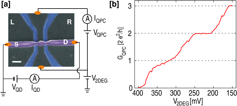
Figure 1(a) shows a scanning electron microscope (SEM) image of the device used in the experiments in this section. An InAs nanowire is deposited on top of a shallow (37 nm below the surface) AlGaAs/GaAs heterostructure based two-dimensional electron gas. The QPC is defined by etched trenches, which separate the QPC from the rest of the 2DEG. The parts of the 2DEG marked by L and R are used as in-plane gates. The horizontal object in the figure is the nanowire lying on top of the surface, electrically isolated from the QPC. The QD in the nanowire and the QPC in the underlying 2DEG are defined in a single etching step using patterned electron beam resist as an etch mask. The technique ensures perfect alignment between the two devices. Details of the fabrication procedure can be found in Ref. [3]. The QD charging energy is around , due to the small size of the structure.
In Fig. 1(b), we plot the conductance of the QPC, measured when shifting the voltage on the part of the 2DEG connected to the QPC () and keeping the other contacts grounded. Making more positive has the same effect as making the surrounding gates more negative, leading to pinch-off of the QPC. As is lowered, the constriction opens up to allow the first electron mode to populate the QPC. Further lowering makes more modes available and the conductance increases stepwise.
1.1 Charge detection
Next, we investigate the electrostatic interactions between the QPC and the QD in the nanowire. Figure 2 displays simultaneous measurements of QPC and QD currents for the structure of Fig. 1(a). As the gate voltage is lowered, electrons are unloaded from the QD and the QD current shows clear Coulomb peaks at each charge transition. At the same time, the QPC conductance changes in steps at the positions of the Coulomb peaks [4]. The QPC was voltage biased with and operated between pinch-off and the first plateau. The QPC conductance is kept roughly constant during the sweep by applying a compensation voltage to the side gate marked by L in Fig. 1(a).
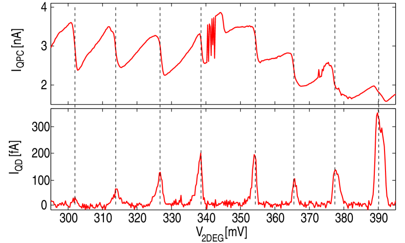
The left-most peak in the QD current in Fig. 2 is barely measurable due to weak tunnel coupling between the QD and its leads. However, the charge transition is still clearly visible in the QPC signal. This demonstrates one of the advantages of the charge detection method compared to a standard current measurement. A conventional current meter has a resolution of , meaning that the tunneling rates of the QD must be kept larger than for reasonable integration times. Moreover, in order to measure current through the QD it needs to be hooked up to two leads. On the other hand, a charge detector can measure electron tunneling which occurs on much slower timescales as well as detect equilibrium fluctuations between a QD and a single lead.
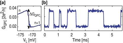
Figure 3(a) shows a measurement of the QPC conductance for a small region around one charge transition in the QD. The measurement was performed without any bias voltage applied to the QD and with the drain lead of the QD pinched off. At , the electrochemical potential of the QD shifts below the Fermi levels of the source lead and an electron may tunnel onto the QD. This gives a decrease of the QPC conductance corresponding to the change of the charge population on the QD. The curve in Fig. 3(a) shows the average QPC conductance, which gives the time-averaged QD population. In Fig. 3(b), we perform a time-resolved measurement of the QPC conductance at . The QPC conductance fluctuates between the two levels corresponding to and electrons on the QD. Transitions between the levels occur on a millisecond timescale, which provides a direct measurement of the tunnel coupling between the QD and the source lead [6].
1.2 Time-resolved operation
As described in the previous section, charge transitions in the QD may be detected in real-time if tunnel couplings between the QD and its leads are tuned below the QPC measurement bandwidth. This allows a wealth of experiments to be performed, like investigating single-electron dynamics or probing interactions between charge carriers in the system. We postpone the detailed investigation of single-electron tunneling in quantum dots to section 2; here we focus on the experimental setup and how to optimize the QPC in order to perform the best possible charge detection measurement. Figure 4(a) shows a time trace of the QPC current, measured in a configuration where the coupling between the QD and the source lead is below , and the other lead is completely pinched off. Again, the QPC current shows two levels, corresponding to and electrons on the QD.
The time resolution available for detecting charge transitions as seen in Fig. 4(a) is set directly by the bandwidth of the QPC measurement circuit. On the other hand, increasing the bandwidth also increases the noise in the measurement, leading to a trade-off between noise and bandwidth. The effect is visualized in Fig. 4, where the two curves show the same set of data but filtered with different bandwidths, (black) and (red). The filtering was performed numerically with a 6th-order Bessel low-pass filter. In Fig. 4(b), we zoom in on one of the transitions of Fig. 4(a). The data taken with lower bandwidth shows a considerably slower time response than the trace taken with higher bandwidth. The lower-bandwidth filter also introduces a time offset; this is not a major problem since we are interested in determining the time intervals between transitions rather than the absolute transition times.
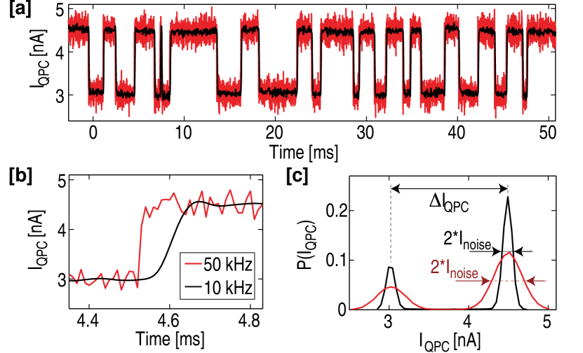
In Fig. 4(c), we plot the distribution functions for the two traces shown in Fig. 4(a). The distributions contain two peaks associated with the two QPC current levels. The distance between peaks gives directly the change in QPC current () for one electron entering the QD, while the standard deviation of the current distribution around each peak () reflects the amount of noise in the measured signal. As a consequence of the increased bandwidth for the red trace, the data contains noise contributions from a broader frequency spectrum and the peaks in the distribution function become significantly broader.
1.3 Signal-to-noise
The ratio between the change in current and the noise is conveniently expressed as a signal-to-noise (S/N) ratio. To maximize the useful information that can be extracted from the measurement, we need to maximize the signal and minimize the noise. In this subsection we consider the effects of the noise, in the following sections we describe how to optimize the signal by tuning the operation point of the QPC.
The noise of the QPC signal can be seperated into intrinsic and extrinsic contributions. With intrinsic noise we refer to noise generated by the QPC itself, while extrinsic noise is due to amplifiers and other external noise sources. It turns out that the main source of noise in the setup is given by amplifier noise. Since the noise is extrinsic, it is essentially independent of both operating point and biasing conditions of the QPC. The only way to reduce this noise is to use an amplifier with lower noise figures or to reduce cable capacitances. The amplifier noise spectrum is not flat and depends on the details of the experimental setup [7, 8]; a rough estimate for the noise contribution in the relevant frequency range is .
The fundamental intrinsic noise of the QPC current is the shot noise, which arises due to the fact that the current is carried by discrete charged particles. The shot noise has a flat power spectrum in the region of interest which scales linearly with the magnitude of the current. For typical currents used here (), the white noise power is , which is considerably lower than the amplifier noise. The thermal noise or Johnson-Nyquist noise is generated by the thermal agitation of the charge carriers in a conductor and appears regardless of applied voltage. Since the sample is held at very low temperatures, its thermal noise becomes negligible compared to the amplifier noise. Another form of intrinsic noise arises because of fluctuations of trapped charges close to the QPC. The charge traps sit at lattice defects or at the heterostructure surface and may be activated by a large current passing the QPC. Such noise is usually referred to as burst noise or popcorn noise. In GaAs QDs, it is believed that the 1/f-noise is generated by fluctuations in an ensemble of charge traps distributed uniformly in the device [9]. The magnitude of the noise depends on the quality of the heterostructure and on the abundance of traps close to the QPC. As we will see later in this section, the charge detection technique provides a method for mapping out the charge traps near the QPC.
The noise is described by a power spectral density , which depends on the physical process responsible for generating the fluctuations. The amplitude of the current noise in a trace as shown in Fig. 4 is given by integrating the spectral density over the measurement bandwidth
| (2) |
Here, is the noise power and the measurement bandwidth. If we assume for simplicity the spectrum to be independent of frequency , then the current noise scales with the square root of the bandwidth,
| (3) |
Increasing the bandwidth thus increases the noise and lowers the S/N, as visualized in Fig. 4. A single-electron detector must be able to reliably detect transitions between the two levels in the QPC current. How much can the bandwidth and the noise be increased before the detection mechanism becomes unreliable? A qualitative answer would be when is comparable to the step height . To investigate the issue quantitatively, we need to estimate the probability of detecting false transitions due to the noise. The problem is well understood in the language of information theory [10]; here we make a simplified analysis to get a quick estimate of the risk of detecting false counts.
For this purpose, we assume the distribution of the QPC current to be Gaussian around each of its two levels and evaluate the part of the distribution deviating by more than from the peak value,
| (4) |
This fraction is beyond the midline between the two peaks of the distribution and gives rise to false counts. The number of false counts registered during a time interval is equal to multiplied with the number of measurements performed in the interval, which according to sampling theorem needs to be . For the false counts, we get
| (5) |
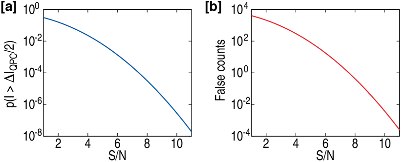
In Fig. 5(a) we plot as a function of S/N. As a consequence of the Gaussian distribution, the risk of detecting false counts falls off stronger than exponential with increased S/N. Figure 5(b) shows the risk of detecting a false count, calculated using Eq. (5) with and . For S/N=7, we find that the detector will register an average of four false counts per second.
1.4 Tuning the QPC operating point
Next, we investigate the best regime for operating the QPC as a charge detector. The conductance of a QPC depends strongly on the confinement potential . When operating the QPC in the region between pinch-off and the first plateau , a small perturbation leads to a large change in conductance . If a QD is placed in close vicinity to the QPC, we expect a fluctuation in the QD charge population to shift the QPC potential and thus give rise to a measurable change in QPC conductance. A figure of merit for using the QPC as a charge detector is then
| (6) |
The first factor describes how the conductance changes with confinement potential, which depends strongly on the operating point of the QPC. The second factor describes the electrostatic coupling between the QD and the QPC and is essentially a geometric property of the system.
The performance of the charge detector depends strongly on the operating point of the QPC. The best sensitivity for a device of given geometry is expected when the QPC is tuned to the steepest part of the conductance curve. This corresponds to maximizing the factor in Eq. (6). In Fig. 6(a) we plot the conductance change for one electron entering the QD versus QPC conductance, in the range between pinch-off and the first conductance plateau (). The change is maximal around but stays fairly constant over a range from 0.3 to . The dashed line in Fig. 6(a) shows the numerical derivative of with respect to gate voltage. The maximal value of coincides well with the steepest part of the QPC conductance curve. The inset in the figure shows how the conductance changes as a function of gate voltage.
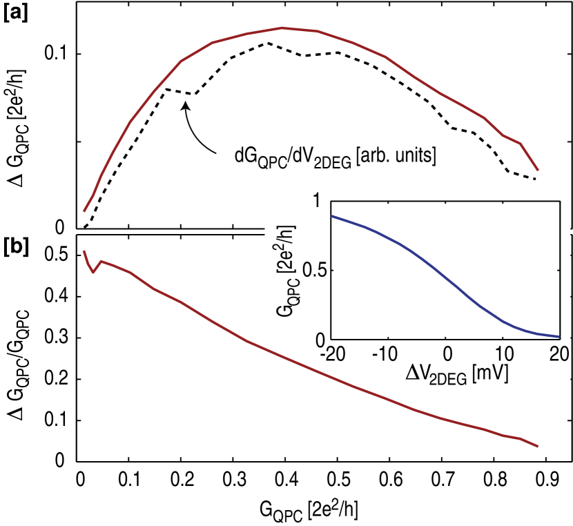
In Fig. 6(b), we plot the relative change in conductance for the same set of data. The relative change increases monotonically with decreasing conductance, reaching above 50% at . The relative change in QPC conductance in this particular device is extraordinarily large compared to top-gate defined structures, where is typically around one percent for the addition of one electron on the QD [7, 11]. We attribute the large sensitivity to the close distance between the QD and QPC (, due to the vertical arrangement of the QD and QPC) and to the absence of metallic gates on the heterostructure surface, which reduces screening.
The results of Fig. 6 indicate that it may be preferable to operate the charge detector close to pinch-off, where the relative change in conductance is maximized. The quantity relevant for optimal detector performance in the experiment is the signal-to-noise (S/N) ratio between the change in conductance and the noise level of the QPC conductance measurement. We measure the conductance by applying a fixed bias voltage across the QPC and monitoring the current. In the linear response regime, both the average current and the change in current for one electron on the QD () scale linearly with applied voltage bias. The noise in the setup is dominated by the voltage noise of the amplifier, which is essentially independent of the QPC operating point and the applied bias in the region of voltages discussed here. The S/N thus scales directly with
| (7) |
In practice the maximal usable QPC current is limited by effects like heating or emission of radiation which can influence the measured system. When considering heating effects, it becomes important to minimize the power dissipated in the QPC. Putting the power dissipation as a constraint to Eq. (7), the highest S/N is reached for the maximal value of . For the data shown in Fig. 6 this occurs at . However, this operation point requires a large voltage bias to be applied to the QPC. If the QPC bias is larger than the single-particle level spacing of the QD, the current in the QPC may drive transitions in the QD and thus exert a back-action on the measured device [12] (see section 5). Therefore, a better approach is to limit the QPC voltage. Here, the best S/N is obtained when optimizing rather than and operating the QPC close to . The sensitivity of the QPC together with the bandwidth of the measurement circuit allows a detection time of around [13].
1.5 Charge traps in the vicinity of the QPC
In the previous sections, we mentioned that charge fluctuations in traps in the vicinity of the QPC may induce excess noise in the QPC current measurement [9]. If the trap is close enough and if the fluctuations occur on a timescale slower than the measurement bandwidth, the charge dynamics of the individual traps can be investigated using the time-resolved charge detection methods. By comparing the conductance change due to charge fluctuations in a trap with the conductance change due to an electron in the QD, we get an idea of the position of the trap relative to the QD. The trap position may be further pinned down by checking the influences of various gate voltages [14].
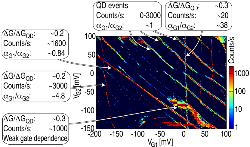
Figure 7 shows electron counts registered by the QPC charge detector for a QD-QPC structure defined by local oxidation [see Fig. 9(a)]. The two voltages and are applied to gates to the left and right of the structure that have roughly the same capacitive lever arms () on the QD states. The lines with slope in Fig. 7 all give the same and thus belong to tunneling in the QD. In the lower-left region of the graph the tunneling in the QD disappears due to pinch-off of the QD leads.
Various other lines are seen in the plot; their gate voltage dependences and their influence on the QPC conductance are given in the figure. Traps with are situated closer to gate G1, traps with are closer to gate G2. The trap with seen to the left in the graph is probably relatively close to the QD; the lines from the trap and the lines from the QD anticross due to their mutual charging energy, similar to a double quantum dot system. Almost all traps give a smaller compared to the QD, showing that the major influence on QPC conductance still originates from the QD. We note that the method only shows traps where the charge fluctuates on timescales slower than the measurement bandwidth; traps with faster fluctuations will give an overall increase in the noise floor.
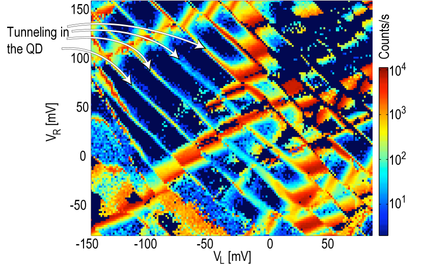
It is not clear whether the charge traps are formed inside the heterostructure or if they are sitting on the surface. In Fig. 8, we present a measurement similar to the one shown in Fig. 7, but this time for a QPC defined by etching [see Fig. 1(a)]. This sample shows a greater trap density compared to the structure defined by local oxidation used in Fig. 7. The difference could be due to the fabrication method; the etching procedure will bring surface states closer to the QPC. For a structure defined by local oxidation, the surface is kept further away. On the other hand, it is dangerous to draw too far-going conclusions from the two sets of data; the structures were fabricated on different (but similar) wafers, and the measurement of Fig. 8 was performed at a higher electron temperature ( compared to ). Further experiments are necessary to clarify the issue.
2 Time-resolved electron transport
In this section, we show how time-resolved charge-detection is used to investigate properties of electron transport in a single quantum dot. We start with describing the dynamics of electron tunneling between one lead and a single QD state, before moving on to more complex situations involving multiple leads, finite bias, excited states and degenerate states. Finally, we show how the potential landscape forming the tunnel barriers is influenced by changing the gate voltages.
2.1 Sample and experimental setup
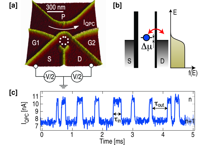
The sample investigated in this section is shown in Fig. 9(a). The structure was fabricated on a GaAs-GaAlAs heterostructure containing a two-dimensional electron gas 34 nm below the surface (density m-2, mobility 25 m2(Vs)-1). An atomic force microscope (AFM) was used to oxidize locally the surface, thereby defining depleted regions below the oxide lines [15, 16].
The sample consists of a QD [dotted circle in Fig. 9(a)] and a nearby QPC. The charging energy of the QD is and the mean level spacing is . From the geometry and the characteristic energy scales, we estimate that the QD contains about electrons. The QD is connected to source and drain leads through tunnel barriers. The transparency of the tunnel barriers is controlled by changing the voltage on gates and . In the experiment, we tune the tunnel coupling rates between the QD and the leads to below 10 kHz. This allows electron tunneling to be detected in real-time with the low-bandwidth () detector. The gate is used to tune the conductance of the QPC to a regime where the sensitivity to changes in the QD charge is maximal. The voltage on gate is adjusted to keep the QPC in the region of maximum sensitivity whenever changing the voltage on another gate. The measurements were performed in a dilution refrigerator with a base temperature of 60 mK.
2.2 Electron tunneling with one lead connected to the quantum dot
First, we investigate the case of electron tunneling between a QD and one lead. This is achieved by keeping the drain barrier open but making the source barrier very opaque, allowing electron tunneling only between the QD and the drain lead [Fig. 9(b)]. Coulomb blockade prohibits the QD to hold more than one excess electron. When an electron enters the QD, the conductance through the QPC is reduced due to the electrostatic coupling between the QD and the QPC. As the electron leaves, the QPC conductance returns to the original value. This gives rise to a QPC current switching between two levels, as shown in Fig. 9(c). The low level corresponds to a situation where the dot holds an excess electron. Transitions between the two levels occur whenever an electron enters or leaves the QD. The duration between transitions gives directly the time it takes for an electron to tunnel into or out of the QD. In Fig. 9(c), these times are marked by and .
In the regime of single-level transport, the process of an electron tunneling into or out of the dot is described by the rate equation
| (8) |
Here, is the probability density for an electron to tunnel into or out of the dot at a time after a complementary event. Solving the differential equation and normalizing the resulting distribution gives
| (9) |
The tunneling rates in Eqs. (8, 9) are effective rates involving the dot-lead tunnel coupling and the thermal population of the states in the lead, with
| (10) | |||||
| (11) |
Here, is the Fermi distribution function, is the electron temperature in the lead and is the energy difference between the electrochemical potential of the QD and the Fermi level in the lead. Equations (10-11) are valid in a small range around where the tunnel coupling can be assumed to be independent of energy and gate voltages. The gate-voltage influence on the tunnel coupling is investigated in greater detail in section 2.6. Also, Eqs. (10-11) assume the QD state to be non-degenerate. In the case of degenerate states, the rates should be multiplied with the appropriate degeneracy factor. Here, we assume non-degenerate states and postpone the discussion of degenerate states to section 2.7.
The method of time-resolved charge detection makes it possible to test the validity of the model described in Eqs. (8-11). The tunneling rates , are determined directly from time traces such as the one shown in Fig. 9(c). Using Eq. 9, we find
| (12) |
where and are the average tunneling times extracted from the time trace. It should be noted that the expression in Eq. (12) is valid only for an infinite-bandwidth detector, and that the finite bandwidth of the detector leads to a systematic under-estimation of the actual rates. However, knowing the bandwidth makes it possible to correct for the deviations [17]. The influence of the detector bandwidth is discussed in greater detail in section 3.7.
Combining Eqs. (10-12) gives an expression for the Fermi function
| (13) |
with being the average excess charge on the QD. The average dot population can be determined by monitoring the average conductance of the QPC [18]. By adding time resolution to the detector and counting electrons one by one as they enter the QD, we can extract not only the Fermi function of the lead but also the tunnel coupling . Assuming sequential tunneling and using Eqs. (10-11), we find that the rate for electrons entering the dot is given by
| (14) |
Measuring the count rate thus directly determines the tunnel coupling .
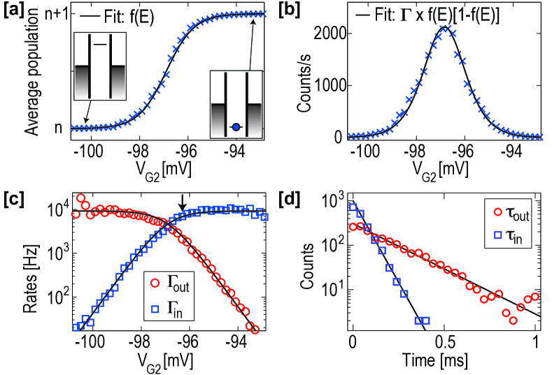
In Fig. 10(a, b) we plot the average QD population and the number of counts per second as gate was used to change the electrochemical potential of the QD. The solid lines are the fits to Eq. (13) and Eq. (14), demonstrating the good agreement between the data and the expected relations. By first determining the lever arm between gate and the dot from standard Coulomb diamond measurements [19], it was possible to extract the electronic temperature () from the width of the Fermi function. The same temperature was found by checking the width of standard Coulomb blockade current peaks [19], measured with the QD in a more strongly coupled regime.
The time-resolved detection method also allows the tunneling rates and to be determined separately. The rates are plotted in Fig. 10(c), extracted from the same set of data as shown in Fig. 10(a, b). The solid lines are fits to Eqs. (10-11), with and . The figure clearly demonstrates an exponential falloff of the tunneling rates as the QD electrochemical potential is shifted above or below the Fermi level of the lead. This is a direct consequence of the Fermi distribution for the electrons in the lead. The fact that both and can be fitted with a single tunneling rate shows that the QD state is non-degenerate. This is not always the case, as will be seen in section 2.7.
The results presented so far rely on the assumption that Eq. (9) is correct. The validity of this assumption can be tested by extracting the experimental distribution function of tunneling times , from a time trace containing a large number of events. Such distributions are shown in Fig. 10(d), taken at the position marked by the arrow in Fig. 10(c). The data exhibit the expected exponential behavior of Eq. (9), with dashed lines being fits with and .
The measurements presented so far only involve tunneling between the QD and one lead. These tunneling events are due to equilibrium fluctuations and do not give rise to a net current through the QD. Consequently, it is impossible to investigate such effects with conventional current measurement techniques. This demonstrates the power of time-resolved charge detection methods for probing properties of mesoscopic structures. The overall good agreement between Eqs. (9-11) and the results of Fig. 10 makes us confident that the model of single-electron tunneling is well capable of describing the system. Next, we move on to the case where the QD is connected to two leads.
2.3 Electron tunneling with two leads connected to the quantum dot
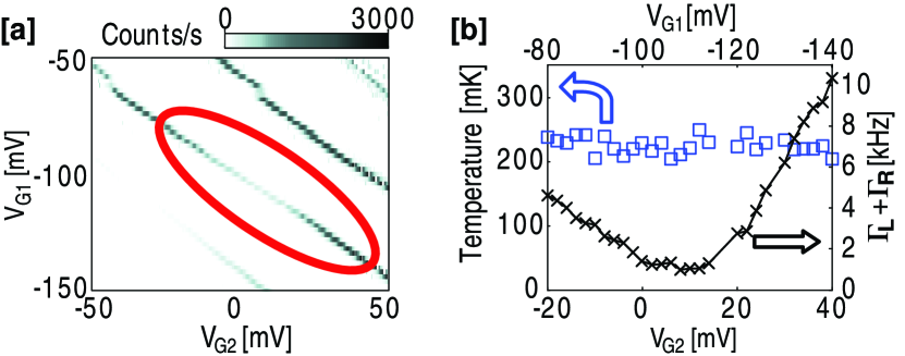
In order to perform time-resolved measurements of electron transport through the dot, the tunnel barriers have to be symmetrized so that both give similar tunneling rates. The rates must be kept lower than the bandwidth of the setup, but still high enough to give good statistics. Figure 11(a) shows the number of events per second as a function of the two gate voltages and . In the upper left corner of the figure, is high and is low, corresponding to the case where the source lead is open and the drain lead is closed. In the bottom right corner, the configuration is inverted. For the region in between, marked by the ellipse in Fig. 11(a), the data indicate that both leads are weakly coupled to the dot.
For zero voltage bias across the QD, the measurement method does not enable us to distinguish whether an electron that tunnels into the dot arrives from the left or from the right lead. Therefore, when both leads are connected to the dot, the rates in Eqs. (10-11) must be adjusted to contain one part for the left lead and one part for the right lead,
| (15) |
Here, and are the Fermi distribution functions of the left and the right lead, respectively. Using Eq. (2.3), we calculate the rate of events for the case when both leads are coupled to the dot with rates accessible for the detector,
| (16) |
With no bias applied across the dot, the two distributions functions and are identical except for a possible difference in electronic temperature in the two leads. However, assuming , we have , and Eq. (16) simplifies to . Fitting this expression to curves similar to that shown in Fig. 10(b), we extract the temperature and combined tunneling rate from the data within the ellipse of Fig. 11(a). The result is presented in Fig. 11(b). The rates and the temperature shown in the graph are due to the combined tunneling to and from both leads. Still, for low /high , the drain lead is pinched off and tunneling occurs mainly between the source lead and the dot. For high /low , the source is pinched off and the tunneling is dominated by electrons going between the drain and the dot. The fact that the electronic temperatures extracted from both regimes turn out to be the same () within the accuracy of the analysis justifies the assumption that .
2.4 Finite bias
With the barriers properly symmetrized, we apply a finite bias voltage between source and drain leads and measure electron transport through the QD. Figure 12(a) shows Coulomb blockade diamonds measured by counting electrons entering the QD. The bias is applied symmetrically, with
| (17) |
The gate is used as a plunger gate to control the dot electrochemical potential. However, the gate also strongly affects the source tunnel barrier. For low voltages, the source lead is closed, giving strong charge fluctuations only when the drain lead is in resonance with the dot [see case I in Fig. 12(a, b)].
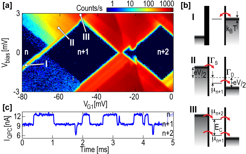
At higher gate voltages, the source lead opens up and a current can flow through the dot. In point II of Fig. 12(a), the QD electrochemical potential lies within the bias window but far away from the thermal broadening of the Fermi distribution in the leads. The condition can be expressed as
| (18) |
where the ”+” case refers to the source contact and the ”-” case refers to the drain. Whenever Eq. (18) is fulfilled, electrons can only enter the dot from the source lead and only leave through the drain. This makes it possible to determine the individual tunnel couplings , with
| (19) |
In this regime, we measure the current through the dot by counting events. This opens up the possibility to use the QD as a very precise current meter for measuring sub-fA currents [21, 22]. Since the electrons are detected one by one, the noise and higher order correlations of the current can also be experimentally investigated. This is explained in more detail in section 3.2
When the bias exceeds the dot charging energy, , and the electrochemical potentials of the and the states are within the bias window [see case III of Fig 12(a,b)], transport processes are allowed where the dot may contain 0, 1 or 2 excess electrons. A time trace measured at point III of Fig. 12(a) is shown in Fig. 12(c). The sensitivity of the QPC charge detector allows to measure switching between three different levels, corresponding to , and electrons on the dot. It is not possible to make this distinction in a standard current measurement.
2.5 Excited states
If there are excited states inside the bias window, tunneling may occur into any of the available states. In this regime, the rates and of Eq. (19) will not be the tunneling rates of the single ground state but rather a sum of rates from all states contributing to the tunneling process. A further complication with excited states is that there may be equilibrium charge fluctuations between the lead and the excited state, thereby removing the unidirectionality of the electron motion. However, if the relaxation rate of the excited state into the ground state is orders of magnitude faster than the tunneling-out rate, the electron in the excited state will have time to relax to the ground state before equilibrium fluctuations can take place.
The separate rates and for a close-up of the upper-left region of Fig. 12(a) are plotted in Fig. 13(a, b). It is important to note that the requirement of Eq. (18) is met only for the region along and above the dashed lines in the figures. At the lower left end of the dashed lines, the energy levels of the dot are aligned as shown in Fig. 13(c). Going diagonally upward along the lines corresponds to raising the Fermi level of the source lead, while keeping the energy difference between the dot and the drain lead fixed.
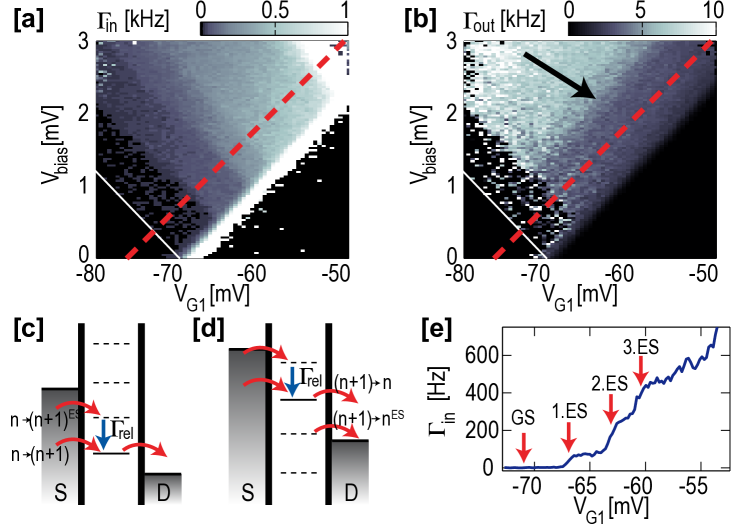
Starting at low bias and low voltage on the gate , the dot is in the Coulomb blockade regime, and no tunneling is possible. Following the dashed line upwards, the QD ground state becomes available for tunneling at . The transition is marked by the white solid lines in Fig. 13(a, b). At these low gate voltages, the source tunnel barrier is almost completely pinched off, meaning that the rate for electrons entering the QD is still low [Fig. 13(a)]. Even so, some electrons do enter the QD, as can be seen from the few points of measurements of within the corresponding region of Fig. 13(b).
We first concentrate on the tunneling-in rate in Fig. 13(a). As the source level is further raised, excited states become available for transport. The first excited state (at along the dashed line) is more strongly coupled to the lead than the ground state, giving a tunneling rate of for electrons entering the dot. The large difference in the tunneling-in rate between the ground and the excited state can be understood if the wavefunctions of the ground and excited state have different spatial distributions. If the overlap with the lead wavefunction is larger for the excited state, the tunneling rate will also be larger. Similar differences in tunneling rates have been found between the singlet and triplet states in a two-electron dot [23, 24].
By further raising the source level, tunneling can also occur through a second excited state. The measured tunneling-in rate will now be the sum of the rates from both excited states; by subtracting the contribution from the first state, the rate for the second state can be determined. Using this method, we can resolve three excited states, with excitations energies , , and with tunneling rates , , . The excited states are clearly seen in Fig. 13(e), which is a cut along the dashed diagonal line in Fig. 13(a).
Focusing on the rates for electrons tunneling out of the QD [Fig. 13(b)], there is a noisy region where the ground state but no excited states are within the bias window ( along the dashed line). In this regime, few electrons will enter the dot, meaning that the statistics needed for measuring the rate of electrons leaving the dot is not sufficient. However, for bias voltages higher than the first excited state, the tunneling-out rate remains constant along the dashed line. This is in contrast to the steps seen in the tunneling-in rates, indicating that the rate for tunneling out of the QD does not depend on the state used for tunneling into the QD. Since the individual excited states are expected to have different rates also for tunneling out of the dot, the data is consistent with the interpretation that an electron entering the dot into an excited state will always have time to relax to the ground state before it tunnels out. The rate for tunneling out is , giving an upper bound for the relaxation time of .
The main relaxation mechanism in quantum dots is thought to be electron-phonon scattering [25]. Measurements on few-electron vertical quantum dots have shown relaxation times of [26]. Recent numerical investigations have shown that the electron-electron interaction in multi-electron dots can lead to reduced relaxation rates [27]. Still, the relaxation rate is expected to be considerably faster than the upper limit we give here.
The rate for tunneling out is actually not constant for the whole region of the Coulomb diamond, but shows a change at the position marked by the arrow in Fig. 13(b). This transition occurs along a line perpendicular to the ones seen in . This is expected assuming the transition seen in Fig. 13(b) involves changes in instead of in . Going perpendicular to the dashed lines in Figs. 13(a, b), we keep the QD and source potential constant while lowering the drain lead. At some point, the Fermi level of the drain is low enough so that an electron in the QD -electron ground state may tunnel out and leave the QD in an -electron excited state. The process is sketched in Fig. 13(d). Comparing Figs. 13(c-d), we see that the rate probes the excitation spectrum of the -electron QD, while reflects the spectrum of the -electron QD.
2.6 Tuning the tunnel couplings
Changing a gate voltage does not only shift the electrochemical potential of the QD, but also affects the height of the tunnel barrier connecting the QD to the leads. The effect was mentioned already in relation with the results of Figs. 11 and 12. Here we investigate the behavior more carefully. Figure 14(a) shows a sketch of the potential landscape for a QD with a bias voltage applied between the source and drain contacts. Electrons entering the QD from the source lead need to tunnel through a potential barrier of height , while the barrier height for electrons tunneling from the QD to drain is . By changing the voltages on gates and , we expect to be able to tune the potentials and and thereby control the tunneling rates.
The tunneling probability also strongly depends on the width of the barrier as well as on the exact shape of the electrostatic potential forming the QD and the barriers. These details are not known, but for small perturbations to the barrier potential and QD potential , the tunneling rate is expected to depend exponentially on the energy difference [28]
| (20) |
Here, and are constants given by the exact shape of the potential. To make quantitative comparisons with the experiments, we use a capacitor model to estimate the influence that gate voltages have on the different potentials in the system [29]
| (24) | |||||
| (32) |
The coefficients are the capacitive lever arms between the gates and the various sample potentials. It should be noted that both the gate voltages , and the source and drain potentials , have gating effects on the QD and on the barriers. In the following, we focus on the influence of the gate voltages , and assume a fixed bias voltage applied symmetrically across the QD, with , . Also, by operating the QD at fixed bias and ensuring that electron transport is unidirectional [Eq. (18)], we can use the relations of Eq. (19) to determine the tunnel couplings and separately.
As seen in Eq. (20), the tunneling strength depends on the difference . To simplify matters we want to fix the QD potential and investigate only the influence that the gate voltages have on the barrier potentials and . This is done by sweeping the two gate voltages and against each other in a way that remains constant. Setting in Eq. (24), assuming a fixed bias voltage () and solving for gives the prescription
| (33) |
Due to the symmetry of the device, we have so that the above expression reduces to . Introducing we find from Eqs. (20-24)
| (34) | |||||
| (35) | |||||
Thus we expect the tunneling rates to depend exponentially on the voltage difference . The sign of the factors and determine if the rates increase or decrease with . From the geometry of the device we expect the source barrier to be more strongly influenced by gate G1 than gate G2 , while the opposite is true for the drain barrier. This would make decrease () and increase () with .
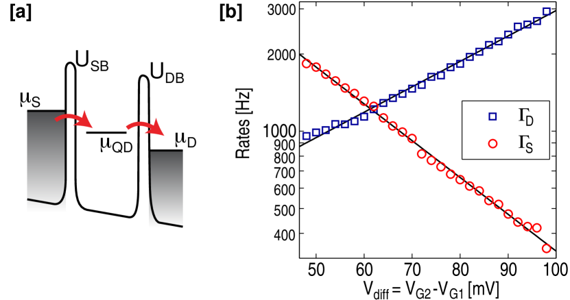
In Fig. 14(b), we plot the tunneling rates and measured while changing . The solid lines are fits to Eq. (35), with fitting parameters and . The results are consistent with Eq. (35), although one would expect from the symmetry of the device. However, the exact shapes of the confining potential and the QD wavefunction are not known and it must be considered unlikely that the potential barriers separating the QD from source and drain contacts are geometrically exactly identical.
2.7 Degenerate states
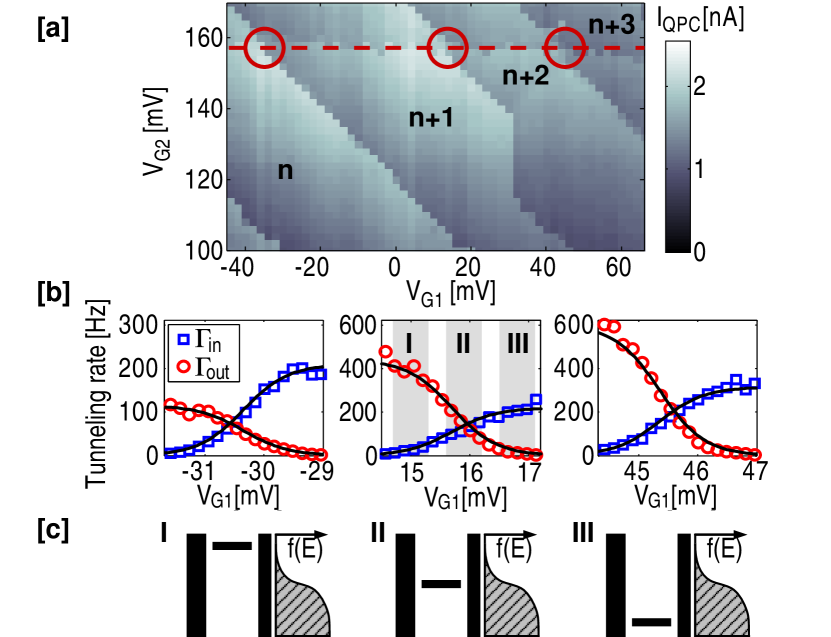
In this section, we discuss how degenerate states may influence the measured statistics. For simplicity, we limit the discussion to the case where the QD is connected only to one lead, with the other lead being completely pinched off. In this configuration, the tunneling is due to equilibrium fluctuations between the QD and the lead. Fig. 15(a) shows the average dc current through the QPC when sweeping the two gates and . The diagonal lines correspond to electrons being loaded/unloaded from the QD. Along these lines, the electrochemical potential of the QD is aligned with the Fermi level of the right lead. From the slope of the line we see that the voltages on the two gates and have roughly the same influence on the energy levels of the QD, as expected from the device geometry. We now focus on determining the tunneling rates for three electronic states along the dotted line in Fig. 15(a). Starting at low voltages, the dot gets successively populated as the voltage on is increased. At each charge degeneracy point, we use the time-resolved measurement techniques to determine the rates for electrons entering and leaving the dot. The results are shown in Fig. 15(b).
Taking the possibility of degenerate states into account, the results of Eqs. (10-11) are extended to
| (36) | |||||
| (37) |
Here, the factors and account for possible degeneracies. For electrons entering the QD, the factor should include the number of degenerate empty states. For tunneling out, only the degeneracy of occupied states is relevant. The tunnel coupling is assumed to be independent of energy and of the QD level within the small gate voltage range considered here. The energy level for three different gate voltages are drawn schematically in Fig. 15(c). The middle plot of Fig. 15(b) indicates the gate voltage ranges corresponding to the drawings shown in Fig. 15(c).
The effective rates for electrons tunneling into and out of the QD involve the density of states and the occupation probability in the lead. This gives a strong dependence on the alignment between the Fermi level in the right lead and the electrochemical potential of the dot. Starting at low voltages in Fig. 15(b) [case I in Fig. 15(c)], the QD potential is far above the Fermi level of the lead. At this point, the density of occupied states in the lead is low and the effective rate for tunneling into the QD is low. If an electron eventually manages to tunnel in, the effective rate for tunneling out again will be high, since there are many empty states in the lead to tunnel into. As the gate voltage is increased, the QD potential goes down to the Fermi level of the lead [case II in Fig. 15(b, c)]. In this configuration, the effective rates for tunneling into and out of the QD are roughly equal. As the gate voltage is further increased, the potential of the QD is pushed below the Fermi level. Here, the density of occupied states in the lead is large, giving a high effective rate for electrons entering the QD. Conversely, the effective rate for leaving the dot is low [case III in Fig. 15(b, c)].
Looking at the shape of the data in Fig. 15(b), we see that they indeed follow a Fermi function. The solid lines in the figure are fits using Eqs. (36-37), with . The parameters used in the fitting procedure are summarized in Table 1.
| -30.35 mV | 210 Hz | 115 Hz | 1.8 |
| 15.70 mV | 220 Hz | 440 Hz | 0.5 |
| 45.35 mV | 315 Hz | 600 Hz | 0.5 |
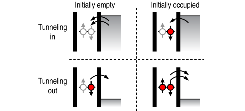
Comparing the numbers of Table 1, we see that the effective coupling differs strongly depending on whether it was extracted from the tunneling in or from the tunneling out data. One possible explanation for the difference is degeneracy due to the electron spin. Assuming a spin-degenerate state with both the spin-up and the spin-down state initially empty, electrons from the lead could tunnel into either of the two states. This makes . Once the electron has tunneled into the QD, it sits in either the spin-up or the spin-down state. Since only one of the spin-degenerate states is occupied, the degeneracy for tunneling out will be . The situation is different if we start with a QD with one of the spin-degenerate states already occupied. For the tunneling-in process, there is only one empty state available, giving . For the tunneling-out process, any of the two electrons sitting on the dot may tunnel out. This leads to . The different situations are shown schematically in Fig. 16. The model discussed here assumes that the spin states are not influenced by Coulomb interactions, which may be an oversimplification considering that we are dealing with a many-electron system. Still, spin pairing has been observed in chaotic QDs containing a large number of electrons [31].
The experimental method described here can only determine the ratio . In the following we assume the degeneracies to be due to spin to be able to extract tunnel couplings and absolute degeneracies from the data. The results of this model are shown in Table 2. For the first resonance at we extract and , indicating a two-fold degeneracy with both states initially empty. At the next resonance, the degeneracy factors are exchanged, with and . For the third resonance, the degeneracy factors are the same as for the second resonance, with and .
| -30.35 mV | 110 Hz | 2 | 1 |
|---|---|---|---|
| 15.70 mV | 220 Hz | 1 | 2 |
| 45.35 mV | 307 Hz | 1 | 2 |
The first and second resonance could be attributed to consecutive filling of spin states, meaning that the two first electrons would form a so-called spin pair. The third electron does not follow the rules expected from simple spin-filling. The reason could be due to many-body effects between the electrons in the quantum dot or due to a charge rearrangement taking place between the second and third resonance (at ). Also, we stress that there are other possible explanations for the measurement results, like energy-dependent tunneling rates or accidental degeneracies of orbital states. To prove the spin degeneracy, one would need to perform measurements at non-zero magnetic fields. This would lift the spin degeneracy and make and .
As seen in section 2.6, changing a gate voltage also affects the tunnel couplings in the system. Since the tunneling rates are measured at slightly different gate voltages, it could be that the differences seen in Fig. 15(b) are due to tuning of the tunneling barrier. To avoid such influences, we used gate to tune the QD electrochemical potential, since it is expected to have a smaller effect on the tunnel barrier between the QD and drain than gate . From Eq. (35) and the results of section 2.6, we estimate the change of tunneling rates within the gate voltage range shown in Fig. 15(b) to be well below . Also, the gating effect of on the tunnel barrier would make it more likely for to increase with . Since is determined at a slightly higher gate voltage than , we would expect to be larger than . This is in contradiction with the results of Table 1 and thus supports our interpretation of additional degeneracies of the QD states influencing the tunneling rates.
3 Statistics of electron transport
In this section, we investigate the statistical properties of single-electron tunneling through a quantum dot. In the general case, we find that current fluctuations due to shot noise are suppressed because of Coulomb blockade. Electrons tend to avoid each other, giving anti-bunching or sub-poissonian noise. In other regimes we find bunching of electrons, or super-poissonian noise. Finally, we investigate how the finite bandwidth of the detector influences the measured statistics and discuss the possibilities of using a quantum dot combined with a charge-detector as a current meter.
3.1 Electron transport and shot noise
Electrical current is carried by electrons passing through the conductor. The current is given as
| (38) |
where is the electron charge and the average time between electrons. The discreteness of the charge carriers gives rise to temporal fluctuations in the current. These statistical fluctuations are called shot noise. The principle behind the shot noise is illustrated in Fig. 17. In Fig. 17(a), we show an idealized current flow. Each spike corresponds to one electron passing the conductor. The time interval between two electrons is constant, so that the current is given as . Figure 17(b) displays a more realistic current, where the time intervals between electrons show random fluctuations. If the average time between electrons , then a measurement of the time-averaged current in case (a) and (b) will give the same value.
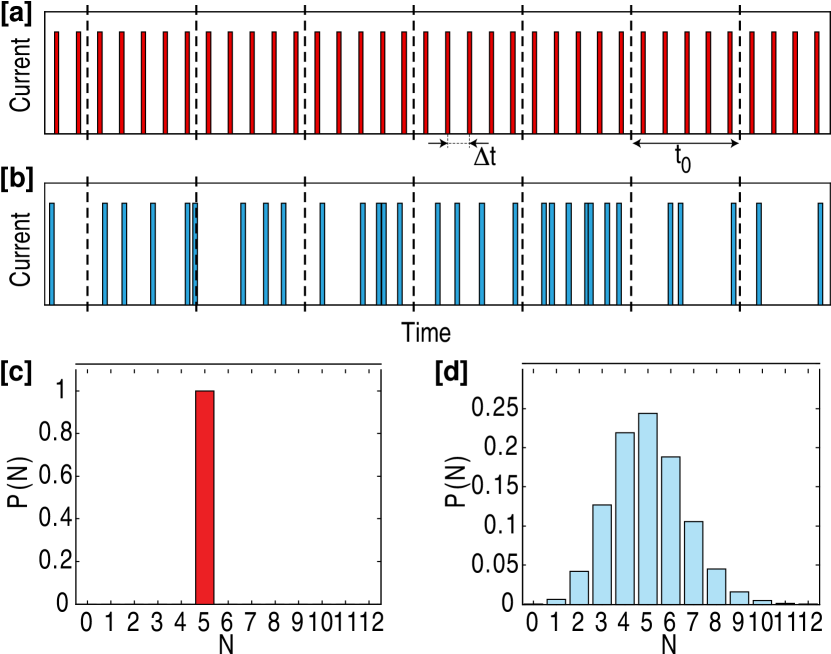
Still, the currents in the two cases are obviously different. This becomes clear in Fig. 17(c-d), where we plot the distribution function of the number of electrons that pass through the conductor within a fixed time-interval . The time is chosen so that the average number of transmitted electron in both cases. The distribution function for the idealized current in (a) is simply a single peak with [Fig. 17(c)]. On the other hand, the realistic current gives a broad distribution due to the statistical fluctuations in the current.
In this way, the shape of the distribution function is a measure of the statistical fluctuations of the current. To be more quantitative, we calculate the central moments of the distribution
| (39) |
Here, represents the mean over a large number of periods of length . The first moment (mean) gives access to the average current, . The second central moment (variance) defines the shot noise power, with
| (40) |
Equation (40) is valid if is much larger than correlation times in the system. In the following section, we will also evaluate the third central moment, . It describes the asymmetry (skewness) of the distribution function around its maximum.
The noise of a current is often expressed as the Fano factor, which is the width of the distribution divided by its mean,
| (41) |
For processes governed by Poisson statistics, like electron tunneling through a single barrier, the Fano factor is equal to one. If the Fano factor is smaller than one, we speak of sub-Poissonian noise. This generally means lower noise power and electron correlation in time. Conversely, if the Fano factor is greater than one, the noise is super-Poissonian and the electron transport is less regular than in the Poissonian case.
If the charge is transferred in units of instead of , the Fano factor will be modified by a factor . By measuring both the shot noise and current , one can use this relation to directly determine the fractionality of the charge of the carriers. Such measurements have been performed to demonstrate the charge of quasi-particles in the fractional quantum Hall effect [32, 33] as well as the double charge of Cooper pairs in superconductors [34]. These are examples where noise measurements provide additional information about the system that can not be extracted from a standard current measurement [35].
In electron transport through a semiconductor quantum dot (QD), the noise is typically suppressed compared to the Poisson distribution. This is due to Coulomb blockade, which enhances the temporal correlation between successive electrons and thereby reduces the noise [36, 37, 38, 39, 40]. The Pauli exclusion principle provides an additional noise suppression mechanism [41, 42]. However, when several channels with different coupling strengths contribute to electron transport, interactions can lead to more complex processes and to an enhancement of the noise [43, 44, 45, 20]. Furthermore, there are predictions that entangled electrons may lead to super-Poissonian noise, thus making noise measurements a possible way of detecting entanglement in mesoscopic systems [46, 47, 48].
The above examples demonstrate that noise measurements are important tools for characterizing properties of mesoscopic systems. However, due to the very low current levels involved, it is difficult to perform the experiments with conventional measurement techniques. One has to carefully eliminate other noise sources like Johnson-Nyquist thermal noise and the noise of the amplifiers. Recent attempts include using a resonant circuit together with a low-temperature amplifier [49, 50], a superconductor-insulator-superconductor junction [51] or a second QD acting as a high-frequency detector [52].
A different approach is to use time-resolved charge detection methods as described in Chapter 2 to count the electrons one-by-one as they pass through the conductor. From such a measurement, one can directly determine the probability distribution function . The distribution function is then used to calculate both the shot noise as well as higher order moments. This way of measuring is analogous to the theoretical concept of full counting statistics (FCS), which was introduced as a new way of examining current fluctuations [53]. In the following sections, we investigate the experimental method in more detail.
3.2 Sequential transport – Sub-Poissonian noise
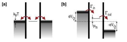
In order to use a charge detector for measuring current and current noise, one has to avoid that electrons tunnel back and forth between the dot and the source or drain lead due to thermal fluctuations [Fig. 18(a)]. This is achieved by applying a finite bias voltage between source and drain, i.e.
| (42) |
Here, is the charging energy, is the electrochemical potential of the QD and is the bias voltage, symmetrically applied to the QD [Fig. 18(b)]. With a finite bias applied to the QD, and with the Fermi levels of the leads far away from the electrochemical potential of the QD, the probability for electrons to tunnel in the opposite direction is exponentially suppressed. In this regime, we attribute each transition to an electron entering the QD from the source contact, and each transition to an electron leaving the QD to the drain contact. The charge fluctuations in the QD then correspond to a non-equilibrium process, and are directly related to the current through the dot. The current is determined by the tunneling rates and , with
| (43) |
From the tunneling rates, one could calculate all the higher moments of the current distribution as well [54]. However, the results are only valid assuming that Eq. (9) is correct. In order to measure the current and the current distribution function for any experimental configuration, we instead focus on extracting the current distribution function from the experimental data.
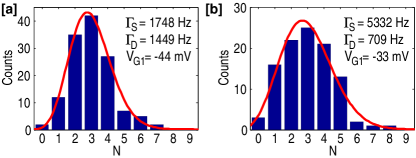
The distribution is found by splitting a time trace of length into intervals of length and counting the number of electrons entering the QD within each interval. Examples of such distributions are shown in Fig. 19, taken at two different gate configurations. The noise and the higher moments are then extracted directly from the measured distribution using Eqs. (39-41), giving for , for case (a) and , for case (b). The noise is relatively close to Poissonian for case (b), but clearly sub-Poissonian in case (a). This difference is easily seen by eye by comparing the width of the two distributions. In order to understand why the shape is different in the two situations in Fig. 19(a, b), we need to calculated the noise expected from the QD. This is the subject of the next section.
3.3 Theory and model description
The noise properties of a QD in the sequential tunneling regime was investigated in detail by Bagrets and Nazarov [54], using the framework of full counting statistics. Here, we summarize their results, apply conditions appropriate for our experimental configuration and compare the theoretical results with experimental data.

The QD occupancy in the low bias, single-level transport regime is modeled by a two-state rate equation
| (44) |
Here, and give the occupation probability for the the states with and electrons, respectively. The two states and the possible transitions are depicted in Fig. 20.
To evaluate the counting statistics of the system, we need to introduce a counting field into the rate equation. We choose to count electrons tunneling into the QD, which changes the matrix in Eq. (44) to:
| (45) |
In the limit , the normalized distribution is independent of . In the same limit, the cumulant-generating function is related to the lowest eigenvalue of , as [54]
| (46) | |||||
The distribution function for the number of electrons tunneling through the quantum dot during a time is generated from the cumulant-generating function [see Appendix A]:
| (47) |
The solid lines in Fig. 19 are distributions calculated from Eqs. (46-47). The tunneling rates and are determined separately, as explained in Chapter 2. The agreement with the experimental distribution is very good, in particular, given that the curves involve no fitting parameters. As mentioned earlier, the graphs show a clear qualitative difference: Figure 19(b) has a broader and more asymmetric distribution than Fig. 19(a). We will see later that this difference comes from the different asymmetries of the source and drain tunneling rates.
In order to perform a more quantitative analysis, we evaluate the three first central moments of the current distribution, which coincide with the first three cumulants [see Appendix A for a discussion about the difference between moments and cumulants]. The cumulants are generated directly from the cumulant-generating function . The mean current is then given by the first cumulant of the distribution:
| (48) |
The symmetrized shot noise is calculated from the variance, or the second cumulant , of the distribution:
| (49) |
from which we get the Fano factor:
| (50) |
where is the asymmetry of the coupling. This result recovers the earlier calculations for the shot noise in a quantum dot [36], and shows the reduction of the noise by a factor for a QD symmetrically coupled to the leads, while the Poissonian limit, , is reached for an asymmetrically coupled QD . The reduction of the noise is a direct consequence of Coulomb blockade; when one electron occupies the QD, a second electron cannot enter before the first one leaves. This leads to correlations in the current fluctuations, and to a reduction of the noise. The reduction is maximal when the tunnel barriers are symmetric. For an asymmetrically coupled QD, the transport is essentially governed by the weakly transparent barrier and the noise approaches the value for a single tunneling barrier, . The results discussed here assume tunneling with transmission coefficients much smaller than one.
Finally, we want to calculate the third cumulant , of the fluctuations, which characterizes the asymmetry of the distribution (skewness):
| (51) |
The asymmetry can also be normalized to the mean of the distribution:
| (52) | |||||
The result shows that for a symmetrically coupled QD, the third moment is reduced by a factor compared to the Poissonian limit. For an asymmetrically coupled dot with , we recover .
3.4 Experimental results
From experimental distributions as the ones shown in Fig 19, we can easily obtain moments of any order using the relations in Eq. (39). We first focus on the mean of the distribution. By measuring as a function of the voltage applied on gate G1 and the bias voltage , we construct the Coulomb diamonds [see Fig. 21(a)]. We observe clear Coulomb blockade regions as well as regions of finite current. Figure 21(b) shows a cross section taken at , the position is indicated by the dashed line in Fig. 21(a)]. As the bias voltage is increased, we see steps in the current. As explained in Section 2.5, the first step in Fig. 21(b) (see left arrow) corresponds to the alignment of the chemical potential of the source contact with the ground state in the QD, and the following steps with excited states in the QD. From the resolution of the Coulomb diamonds, we see that the sample is stable enough such that background charge fluctuations do not play a significant role on the time scales relevant for this experiment [9].
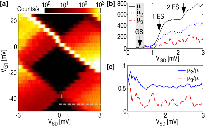
In addition to the mean, we evaluate the second and third central moments from the measured counting statistics. These two moments are plotted in Fig. 21(b) as a function of the bias voltage. The second moment (blue dotted line) reproduces the steps seen in the current. These two moments can be represented by their reduced quantities (Fano factor) and , as shown in Fig. 21(c). Both normalized moments are almost independent of the bias voltage, and show a reduction compared to the values expected for classical fluctuations with Poissonian counting statistics.
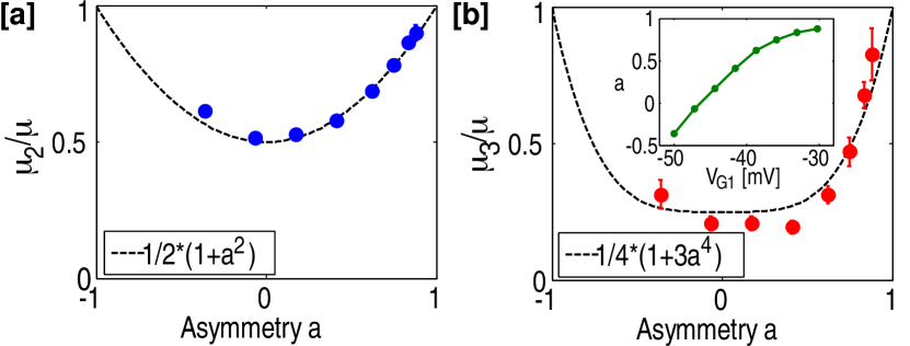
As described in section 2.6, the tunnel couplings can be tuned by adjusting the gate voltages and . In this way, we are able to continuously change the symmetry of the barriers from symmetric to very asymmetric coupling. In Fig. 22, we show the normalized second and third central moments as a function of the asymmetry . The tunneling rates are directly measured as described in section 2, and the inset of Fig. 22(b) shows the variation of asymmetry with gate voltage in the region of interest. As expected from the discussion in the previous section, the noise is reduced for symmetric barriers. The experimental data follow the theoretical predictions given by Eqs. (50, 52) very well. We note in particular that no fitting parameters have been used since the tunneling rates are determined separately.
3.5 Time statistics
A complementary way of investigating the correlations is to look at the temporal statistics of electron transport. Instead of evaluating the probability distribution for the number of electrons that are transferred within a fixed time , we examine the continuous distribution describing the time needed for a fixed number of electrons to pass through the QD. With the rates for tunneling into and out of the QD given by Eq. (9), we find for
| (53) | |||||
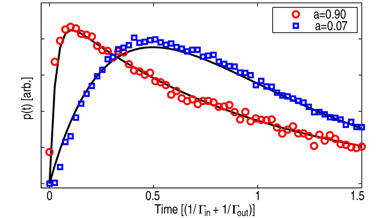
In Fig. 23, we show the experimentally determined distribution for two different values of the asymmetry together with the results of Eq. (53). For the symmetric case [ in Fig. 23], there is a clear suppression of transfer probability for short time scales. Again, this is due to Coulomb blockade. We measure anti-bunching of electrons and sub-Poisson noise levels. For the more asymmetric case [ in Fig. 23], anti-bunching is less prominent and the probability distribution approaches the exponential behavior expected for a single tunnel barrier.
The ability to measure the counting statistics of electron transport relies on the high sensitivity of the QPC as a charge detector. Given the bandwidth of our experimental setup, kHz, the method allows to measure currents up to fA, and we can measure currents as low as a few electrons per second, i.e., less than 1 aA. The low-current limitation is mainly given by the length of the time trace and the stability of the QD, and is well below what can be measured with conventional current meters. In addition, as we directly count electrons one by one, this measurement is not sensitive to the noise and drifts of the experimental setup. It is also a very sensitive way of measuring low current noise levels. The precision and limitations of the measurement method are described in more details in sections 3.7 and 3.8.
3.6 Bunching of electrons
So far, we have analyzed data where the tunneling events can be well explained by a rate equation approach with one rate for electrons tunneling into and another rate for electrons leaving the dot. For the trace shown in Fig. 24(a), the behavior is distinctly different. The electrons come in bunches; there are intervals where tunneling occurs on a fast time scale (), in-between these intervals there are long periods of time () without any tunneling. The data was taken with a bias applied so that the Fermi level of the source lead lines up with the electrochemical potential of the dot, while the drain lead is far below the electrochemical potential of the dot, thus prohibiting electrons from entering the QD through the drain lead. The voltage on gate was set to , which is outside the range of the Coulomb diamonds presented in Fig. 21(a). Since the QPC current is at the high level during the intervals without tunneling, the dot contains one electron less when the fast tunneling is blocked.
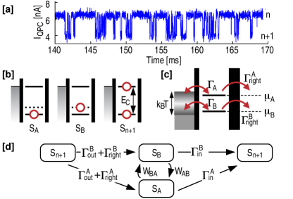
In order to explain the two different time scales, we assume a mechanism where there are two almost energy-degenerate dot states within the thermal broadening of the distribution in the source lead. Because of Coulomb blockade, the dot may hold one or zero excess electrons. Hence, the model includes three possible dot states as shown in Fig. 24(b). State is the -electron ground state, state is an excited -electron state and state is the ground state when the dot contains electrons. Transitions between the / states and the state occur whenever an electron tunnels into or out of the dot.
The tunnel coupling strength between the dot and the lead is given by the overlap of the dot and lead electronic wavefunctions. Since the wavefunctions corresponding to the two states and may have different spatial distributions, the coupling strength of the transition may differ from the coupling of the transition. The energy levels of the dot and the leads for the configuration where we measure bunching of electrons are shown in Fig. 24(c), while the possible transitions of the model are depicted in Fig. 24(d).
Starting with one excess electron on the dot [state in Fig. 24(d)], at some point an electron will tunnel out, leaving the dot in either state or state . Assuming , it is most likely that the dot will end up in the excited state . If the tunneling rate is faster than the relaxation process , an electron from the lead will have time to tunnel onto the dot again and take the dot back to the initial state. The whole process can then be repeated, leading to the fast tunneling in Fig. 24(a).
However, at some point the dot will end up in state , either through an electron leaving the dot via the transition, or through relaxation of the state. To get out of state , there must be either a direct transition back to state , or an electron tunneling into the dot through the transition. With and assuming , both processes are slow compared to the tunneling between the lead and state . This mechanism will block the fast tunneling and produce the intervals without switching events seen in Fig. 24(a). Similar arguments can be used to show that the blocking mechanism will be possible also if .
From the above reasoning, we see that the fast time scale is set by the fast tunneling state, while the slow time scale is determined either by the relaxation process or by the slow tunneling rate, depending on which process is the fastest. Either way, it is crucial that the relaxation rate is slower than the fast tunneling rate (in our case ). We speculate that the slow relaxation rate may be due to different spin configurations of the two states. For a few-electron QD, spin relaxation times of have been reported [23, 55, 56].
To make quantitative comparisons between the model and the data, we use the methods of full counting statistics to investigate how the dot charge fluctuations change as the source lead is swept over a Coulomb resonance. Theoretical investigations of multi-level quantum dots have lead to predictions of electron bunching and super-Poissonian noise [45]. Following the lines of Refs. [54, 45], we first write the master equation for the system,
| (54) |
with
| (55) |
Here and , and are occupation probabilities for states , and , respectively. The effective tunneling rates are determined by multiplying the tunnel coupling constants for each state with the Fermi distribution of the electrons in the lead,
| (56) |
The tunneling rates and are included to account for the possibility for electrons to leave through the right barrier. The Fermi level of the right lead is far below the electrochemical potential of the dot, so that the states in the right lead can be assumed to be unoccupied. Finally, and are the direct transition rates between states and . These rates obey detailed balance,
| (57) |
The phenomenological relaxation rate between the two states is given as .
In Eq. (55), we introduce charge counting by multiplying all entries of involving an electron leaving the dot with the counting factor [54]. We do not distinguish whether the electron leaves the dot through the left or the right lead. In this way we obtain the counting statistics , which is the probability for counting events within the time span . The distribution describes fluctuations of charge on the dot, which is exactly what is measured by the QPC detector in the experiment. We stress that this distribution is equal to the distribution of current fluctuations only if it can be safely assumed that the electron motion is unidirectional. This is the case if the condition in Eq. (42) is fulfilled, i.e. if the tunneling due to thermal fluctuations is suppressed. Here, we are in a regime where there is a mixture of tunneling due to the applied bias and tunneling due to equilibrium fluctuations. But since the model defined in Eq. (55) is valid regardless of the direction of the electron motion, it can still be used for analyzing the experimental data.
Using the method of Ref. [54], we calculate the lowest eigenvalue of and use it to obtain the cumulant generating function (CGF) for ,
| (58) |
The CGF can then be used to obtain the cumulants of any order using the relation . In order to compare the theory with the experiment we extract the first three cumulants of from the experimental data. The cumulants were found by taking a trace of length and splitting it into independent traces. By counting the number of electrons leaving the dot in each trace and repeating the procedure for all sub-traces, the distribution function could be experimentally determined. The experimental cumulants were then calculated directly from the measured distribution function. The time was chosen such that .
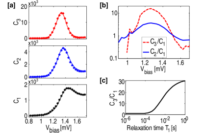
Figure 25(a) shows the first three cumulants versus voltage applied to the source lead. The points correspond to experimental data, while the solid lines show the cumulants calculated from the CGF of our model, with fitting parameters , , , , and . The electronic temperature in this measurement was 400 mK. The figure shows good agreement between the model and the experimental data.
Figure 25(b) shows the normalized cumulants and for the experimental data; we notice that both the second and the third cumulants vastly exceed the first cumulant when the Fermi level of the source lead is aligned with the electrochemical potential of the dot (). For a Poissonian process one expects ; here, the noise is clearly of super-Poissonian nature, as expected from the bunching behavior of the electrons.
When the bias voltage is further increased (), the source lead is no longer in resonance with the electrochemical potential of the dot and the equilibrium fluctuations between the source and the dot are suppressed. In this regime, the measured charge fluctuations are due to a current flowing through the dot. Electrons enter the dot from the source lead and leave the dot through the drain lead. The blocking mechanism is no longer effective and the transport process will predominantly take place through state , since the tunnel coupling to the drain lead is stronger for this state (). The transport through the dot can essentially be described by a rate equation, with one rate for electrons entering and another rate for electrons leaving the dot. For such systems, it has been shown in section 3.2 that the Coulomb blockade will lead to an increase in correlation between the tunneling electrons compared to a single-barrier structure, giving sub-Poissonian noise [36, 40]. The effect is seen for in Fig 25(b); both the second and third cumulants are reduced compared to the first cumulant.
The value of obtained from fitting the experimental data is of the same order of magnitude as previously reported values for the spin relaxation time . We stress that the bunching of electrons and the super-Poissonian noise can only exist if the relaxation time is at least as long as the inverse tunneling time. This is demonstrated in Fig. 25(c), which shows the maximum value obtained for the ratio calculated for different while keeping the rest of the fitting parameters at the values given in the caption of Fig. 25.
3.7 Higher order moments and limitations of the detector
So far, we have presented measurements of the second and third cumulants or central moments. As mentioned in section 3.1, the shot noise is a direct consequence of the discreteness of the charge carriers in the system. A measurement of the second moment (Fano factor) thus provides a way to determine the charge of those discrete carriers. The third moment of a tunneling current has been shown to be independent of the thermal noise [57, 22], thus making it a potential tool for investigating electron-electron interactions even at elevated temperatures.
What about the higher order moments? In strongly interacting systems, they are predicted to depend strongly on both the conductance [58] and on the internal level structure [45] of the system. Determining higher order moments may therefore give a more complete characterization of the electron transport process. This can be of importance for realizing measurements of electron correlation and entanglement effects in quantum dots [46, 47]. In quantum optics, higher order moments are routinely measured in order to study entanglement and coherence effects of the electromagnetic field [59].
In this section, we present measurements of the fourth and fifth cumulant of the distribution function for charge transport through a QD. As demonstrated in section 3.2, we determine the cumulants by first generating the experimental probability density function . This is done by splitting a time trace of length into intervals and counting the number of electrons entering the dot within each interval. The higher cumulants describe more subtle features of the distribution function. To extend the methods of section 3.2 to higher cumulants, it is therefore necessary to increase the measurement time to collect more statistics. This requires a stable sample without any fluctuating charge traps close to the QD.
In the experiment, we use a single QD with the same design as the one described in section 2 and section 3.2. The coupling between the QD and the QPC was weaker in the sample used here, meaning that the bandwidth had to be reduced below . On the other hand, the stability of the structure allowed the measurement of time traces of length . In the experiment, the QPC was voltage biased with . The current signal was sampled at , software filtered at using an 8th order Butterworth filter and finally resampled at in real-time to keep the amount of data manageable.
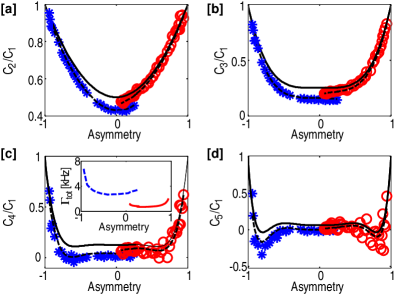
The results are shown in Fig. 26, where we plot the normalized cumulants for different values of the asymmetry of the tunneling rates, . The asymmetry is tuned by shifting the voltage on gate by an amount and at the same time applying a compensating voltage on gate . With the two gates having a similar lever arm on the dot, the electrochemical potential of the QD remains at the same level, but the height of the tunneling barriers between the dot and the source and drain leads will change. Doing so, we could tune the asymmetry from to while still keeping both tunneling rates within the measurement bandwidth and avoiding charge rearrangements. To get data for the full range of asymmetry, we did a second measurement at a different gate voltage configuration. For the second set of data, the asymmetry was tuned from to . The stars and the circles in Fig. 26 represent data from the two different sets of measurements. The measurements were performed with a QD bias of , with the electrochemical potential of the dot far away from the Fermi levels of the source and drain leads. This is to ensure that tunneling due to thermal fluctuations is sufficiently suppressed.
The solid lines in Fig. 26 depict the theoretical predictions calculated from a two-state model [54]. The analytical expressions are given in the figure caption. The higher cumulants show a complex behavior as a function of the asymmetry, with local minima at for and at for . The fifth cumulant even becomes negative for some configurations. The experimental data qualitatively agrees with the theory, but for small values of the asymmetry there are deviations from the expected behavior. The deviations are stronger for the first set of data (stars). Since the tunneling rates in the first measurement was about a factor of three higher than in the second measurement [see inset of Fig. 26(c)], we suspect the finite bandwidth of the detector to be a possible reason for the discrepancies.
In general, experimental measurements of FCS for electrons are difficult to achieve due to the need of a sensitive, high-bandwidth detector capable of resolving individual electrons [61, 62, 21]. However, a more fundamental complication with the measurements is that most forms of the FCS theory assume the existence of (1) a detector with infinite bandwidth and (2) infinitely long data traces. Since no physical detector or experiment can fulfill these requirements, every experimental realization of the FCS will measure a distribution which is influenced by the properties of the detector. In the following, we investigate how the violation of the two assumptions modifies the measured statistics.
Naaman et al. [17] pointed out that measurements of the transition rates of a Poisson two-state system using a finite bandwidth detector always leads to an underestimate of the rates. As a result, the measured probability distribution for the times needed for an electron to tunnel into or out of the QD no longer follow the expected exponential . Due to the finite detection time, very fast tunneling events are less likely to be detected, giving a cut-off for short time scales in the measured distribution. Moreover, since the fast events are not detected, the measurement will over-estimate the occurrence of slow events. The long-time tail of the measured distribution will still decay exponentially, but the tunneling rate extracted from the distribution will be under-estimated. To determine the rates correctly, the detection rate of the detector must be taken into account [17].
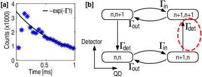
An example of a probability distribution taken from measured data is shown in Fig. 27(a). The long-time behavior is exponential, but for times there is a sharp decrease in the number of counts registered by the detector. From the figure, we can estimate , which is the average time it takes for the detector to register an event. We find , giving a detection rate of . Note that the detection rate does not only depend on the measurement bandwidth but also on the signal-to-noise ratio of the detector signal as well as the redundancy needed to minimize the risk of detecting false events [63]. The compensations for the tunneling rates are given as [17]
| (59) | |||||
| (60) |
Here, are the true tunneling couplings and are rates extracted from the measurement. All tunneling rates presented in the following have been extracted using Eqs. (59-60) with .
The finite bandwidth will also influence the FCS measured by the detector. Following the ideas of Ref. [17], we account for the finite bandwidth by including the states of the detector into the two-state model of section 3.3. Figure 27(b) shows the four possible states of the combined dot-detector model. The state refers to a situation where there are electrons on the dot, while the detector at the same time reads electrons. The transition from the state to the state occurs when the detector registers the electron. This process occurs with the rate of the detector, .
To calculate the FCS for the QD-detector system, we write the master equation , with and
| (61) |
In the above matrix, we have included the counting factor at the element where the detector registers an electron tunneling into the dot [see dashed circle in Fig. 27(b)]. The statistics obtained in this way relates directly to what is measured in the experiment. Using the methods of Ref. [54], we calculate the first few cumulants for the above expression as a function of relative bandwidth and asymmetry . The normalized second and third cumulants take the form
| (62) | |||||
| (63) | |||||
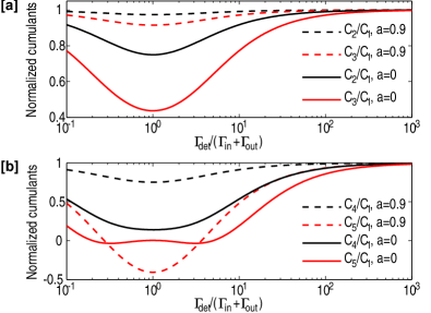
In Fig. 28(a) we plot the second and third cumulants from Eq. (62) and Eq. (63) for different values of asymmetry and relative bandwidth . The cumulants have been normalized to the values for the infinite bandwidth detector. Fig. 28(b) shows the corresponding results for the forth and fifth cumulants. With , the cumulants approach the infinite bandwidth result, as expected. However, even with and perfect symmetry (), the second cumulant deviates by almost 10% and the third cumulant by more than 20% from the perfect detector values. As the bandwidth is further decreased, the deviations grow stronger and reach a maximum as . With , the cumulants once again approach the perfect detector values. When the detector is much slower than the underlying tunneling process, it will only sample the average population of the two states. In this limit, the dynamics of the system does not interfere with the dynamics of the detector and we recover the correct relative noise levels. It should be noted that this is true only for the noise relative to the detected mean current. Since the detector will miss most of the tunneling events, the absolute values of both the current and the noise will be underestimated.
Over the full range of bandwidth and asymmetry, we find that the noise detected with the finite bandwidth system is always lower than for the ideal detector case. The reduction can be qualitatively understood by considering the probability distribution . The finite bandwidth makes it less probable to detect fast events, meaning that the probability of detecting a large number of electrons within the interval will decrease more than the probability of detecting few electrons. This will cut the high-count tail of the distribution and thereby reduce its width () and its skewness (). An interesting feature is that the cumulants calculated for a less symmetric configurations [ in Fig. 27(c)] show less influence of the finite bandwidth.
A second limitation of a general FCS measurement is the finite length of each time trace. In order to generate the experimental probability density function , the total trace of length must be split into intervals, each of length . Most FCS theories only predict results for the case , where is a typical transition rate of the system. In the experiment, it is favorable to make as short as possible in order to increase the number of samples . This will improve the quality of the distribution and help to minimize statistical errors. However, if is made too short, this will influence the extracted distribution. This is visualized in Fig. 29, where distribution functions for different are extracted from the same set of experimental data. The distributions give the same current , but their properties are clearly different. In the extreme case of , the distribution approaches the Bernoulli distribution, for which only and are non-zero.

The condition is imposed by the approximation that the cumulant generating function (CGF) for only depends on the lowest eigenvalue of the master equation matrix , with . A FCS valid for finite must include all eigenvalues and eigenvectors of [54]. The corresponding expression is
| (64) |
where and are the left and right eigenvectors of the matrix , are the eigenvalues of and are the eigenvectors corresponding to the lowest eigenvalue . The cumulants generated from the CGF in Eq. (64) will in general be a function of .
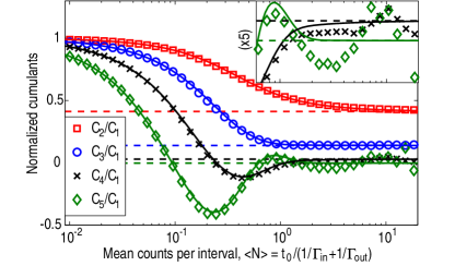
To investigate how small can be before systematic errors become relevant, we calculate the cumulants from the CGF of Eq. (64) with the master equation matrix of Eq. (61). The results are shown in Fig. 30, where we plot the normalized cumulants as a function of the mean number of counts per interval, . The symbols show cumulants extracted from measured data (, , and ), while the solid lines are results from the CGF for the same set of parameters. The dashed lines are the asymptotes for the limiting case .
In general, data and theory are in good agreement. There are some deviations in the fourth and fifth cumulants for large ( in Fig. 30), but these are statistical errors in the experiment due to the finite length of the total time trace. For short , all cumulants converge to . This is because as , the probability distribution will be non-zero only for and , with , and . This is the definition of a Bernoulli distribution, for which the normalized cumulants as [64].
Focusing on the other regime, , we see that cumulants of different orders converge to their asymptotic limits for different values of . The second cumulant needs a longer interval to reach a specified tolerance compared to the higher cumulants. This is of interest for the experimental determination of higher cumulants. By choosing a shorter value of when calculating higher cumulants, the amount of samples can be increased. For the data in Fig. 26, the cumulants were calculated with intervals giving for , for , for and for . The maximal deviations between the correct cumulants and the ones determined with a finite length can be estimated by checking the convergence for all values of the asymmetry. For the data shown in Fig. 26, we find , , and .
Coming back to the results of Fig. 26, we are now able to explain why the measured cumulants show lower values compared to the perfect-detector theory. The dashed lines in Fig. 26 are the cumulants calculated from the combined QD-detector model of Eq. (61), with . The overall agreement is good, especially since no fitting parameters are involved. Higher cumulants end up to be slightly lower than theory predicts. We speculate that the deviations could be due to low-frequency fluctuations of the tunneling rates over the time of measurement.
3.8 Measurement precision
In this section we investigate the precision possible to achieve with a current meter based on single-electron counting. For this purpose, we assume a QD in the high-bias regime with a single state available for transport, i.e., the model defined by Eq. (44) in section 3.3. As derived in section 3.3, the current and the shot noise are
| (65) |
| (66) |
When counting electrons passing through the QD, we use the tunneling electrons to probe the tunnel couplings . Since tunneling is a statistical process, it involves a certain degree of randomness and we need to detect an ensemble of electrons in order to be able to form the average . The statistical variations of the tunneling times imply that there is relation between the duration and the precision of the measurement. More precisely, assuming that the tunneling rates in Eqs. (65-66) are constant, for how long is it necessary to measure in order to reach a certain precision in the current or the noise level? This is investigated in the following section. The theoretical findings are then compared with experimental results.
3.9 Theoretical precision
In the single-level regime, the process of an electron tunneling into or out of the dot is described by the rate equation
| (67) |
Here, is the probability density for an electron to tunnel into or out of the dot at a time after a complementary event. Since the expressions for electrons entering and leaving the dot are the same, we drop the subscripts () and use the notations and to describe either one of the two processes. Solving the differential equation and normalizing the resulting distribution gives
| (68) |
In the experiment, we measure a time trace containing a sequence of tunneling times , To estimate and its relative accuracy from such a sequence, we need to calculate the probability distribution for extracting a certain value , given a fixed sequence of tunneling times. We start by dividing the time axis into bins of width and number them with A tunneling event will be counted in bin if . Using Eq. (68) and assuming , we find that the probability to get a count in bin for a given value of is equal to
| (69) |
A certain sequence is realized with probability
| (70) | |||||
Here, is the number of times an event falls into bin , is the total number of events in the trace and is the average of . A certain set of bin occupations can be achieved with many different -series, namely . Assuming that they all occur with the same probability , we find
| (71) |
This is our sampling distribution. For an estimate of we use Bayes theorem
| (72) |
Because we have no information on the prior probabilities and , the principle of indifference requires them to be constants, giving
| (73) |
where is constant. Normalization leads to
| (74) | |||||
The most likely value of is therefore . The relative accuracy of this estimate is given by the width of the distribution. Setting and evaluating the width at half maximum gives
| (75) |
For large we can expand in a Taylor series around . Keeping only the first two terms, it follows
| (76) |
Thus the relative accuracy is
| (77) |
3.10 Experimental precision
In order to compare the results of Eq. (77) with the measurement, we take a data set containing 120000 events, extracted from a trace such as the one shown in Fig. 9(c). The tunneling rates are and . In the following, we choose to investigate the precision of and drop the subscript. We have also performed the analysis for , with similar results.
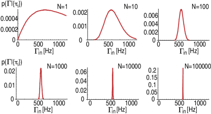
To proceed, we use Eq. (68) to calculate the probability that a certain set of tunneling times belongs to a physical process characterized by the tunnel coupling
| (78) |
In Fig. 31 we plot the probability distributions of Eq. (78) for subsets of with different lengths . As the size of the subset is increased, the probability distribution gets focused around . This simply reflects the fact that the larger the amount of experimental evidence available, the less likely it becomes that the data is generated by a tunneling process with .
The experimental uncertainty in is given by the width of the distributions in Fig. 31. Figure 32 shows the normalized uncertainty versus subset size . The solid line is the result of Eq. (77), showing very good agreement with the experimental data. The results validate Eq. (68) and demonstrate the stability of the sample; a sudden change in the tunnel coupling during the relatively long measurement time of 10 minutes would introduce deviations between Eq. (77) and the measured precision. For the full data set , we find and .
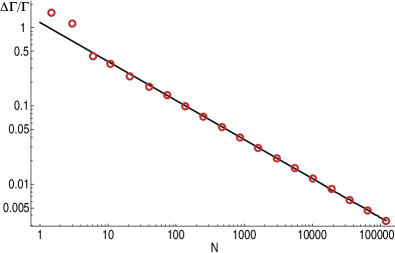
For simplicity, we have assumed a perfect detector with infinite bandwidth. We have also performed the analysis for a model incorporating the detector bandwidth as explained in section 3.7, and we obtain very similar results. The analysis is slightly more involved since a tunnel coupling will depend not only on the set , but also on .
3.11 Current meter precision
Knowing the precision of the tunneling rates , we use the relations in Eqs. (65-66) to determine the precision of the current and the noise. For the data set with discussed in the previous section, we find
| (79) |
The shot noise of the current is equal to
| (80) |
Conventional measurement techniques are usually limited by the current noise of the amplifiers (typically A2/Hz) [32, 33, 37, 39]: here we demonstrate a measurement of the noise power with a sensitivity better than A2/Hz. The limits in precision investigated here are not due to a measurement apparatus but appears because of the discreteness of charge; the precision of the shot noise measurement is limited by the shot noise itself. In the experiment more uncertainty occurs if (1) the correction for the finite bandwidth in Eq. (59) is incorrect or (2) because of the detection of false events due to an insufficient signal-to-noise ratio in the measurement of the QPC conductance (see section 1.3).
4 Double quantum dots
The double quantum dot is the mesoscopic analogue of a diatomic molecule. In weakly coupled dots, the electrons are well localized within the individual dots, their wavefunctions are spatially separated and electron transport is described by sequential tunneling between discrete single-dot states. With increased interdot coupling, the single-dot wavefunctions hybridize and form molecular states extending over both dots. The ability to tune both the interdot coupling and the energy levels of the individual QDs make the double quantum dot an interesting model system for studying interactions in coupled quantum systems. In this section we show how to use time-resolved charge detection techniques to probe various properties of double quantum dots.
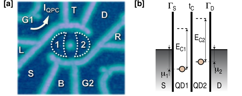
The measurements presented in this section were performed on the sample shown in Fig. 33(a). The structure is fabricated with local oxidation techniques and consists of two QDs (marked by 1 and 2 in the figure) connected by two separate tunnel barriers. For the results presented here only the upper tunnel barrier was kept open; the lower was pinched-off by applying appropriate voltages to the surrounding gates. For the purpose of this section, the system may be described as a standard serial double quantum dot (DQD); the ring-shape properties of the sample are investigated and utilized in section 6.
The DQD is coupled to source and drain leads via tunnel barriers. Several in-plane gates [marked by T, B, L and R in Fig. 33(a)] are used to tune the various tunnel couplings. Two quantum point contacts are located in the upper-left and lower-right parts of Fig. 33(a). In the measurement, it was only possible to operate the upper-left QPC as a charge detector; the one in the lower-right corner was always pinched off. The conductance of the upper-left QPC was measured by applying a bias voltage of and monitoring the current ( in the figure). The QPCs were also used as in-plane gates to control the electron population in the DQD. This was achieved by applying fixed voltages , to both sides of the QPCs in addition to the bias voltage.
In Fig. 33(b) we sketch the energy levels in the system. The QD states are coupled to source and drain leads with tunneling rates and , while the interdot coupling is described by a coupling energy . The electrochemical potentials of the two QDs are denoted by and , measured relative to the Fermi levels of the source and drain leads. The next unoccupied QD states are separated by the charging energies and .
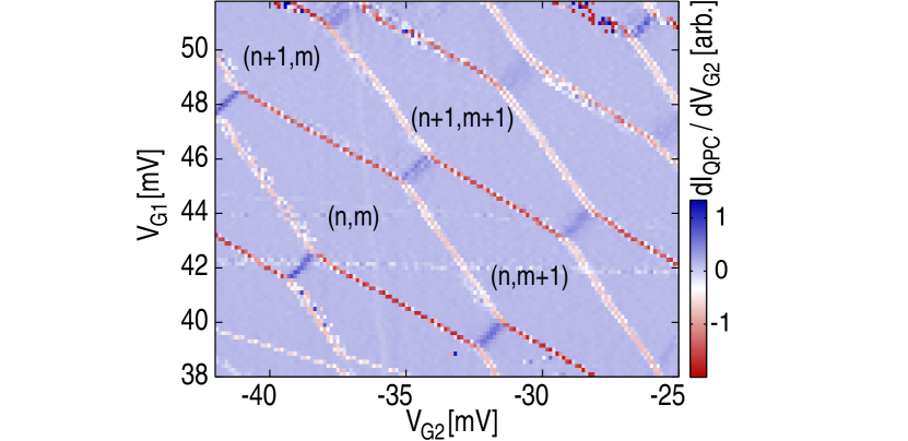
To reach a well-defined DQD configuration we apply negative gate voltages in order to close the constrictions between QD1 and QD2. The gate voltages also influence the tunneling coupling to source and drain; as a consequence the DQD current drops below the measurable limit and we need to operate the charge detector to measure charge transitions in the QDs. Figure 34 shows the numerical derivative of the QPC current with respect to the gate voltage . A compensation voltage was applied to the QPC gate [upper-leftmost part of Fig. 33(a)] to keep the QPC conductance relatively constant within the gate voltage of interest. This gives the uniform light-bluish background of Fig. 34. On top of that there is a clear hexagon pattern emerging, with all features expected from a DQD [65].
The numbers in brackets denote the electron population of the two QDs. The charge transitions occurring at the borders between different regions of fixed charge give rise to different changes of . To understand these features we first note that the QPC is asymmetrically positioned with respect to the DQD, with QD1 being much closer than QD2. Charge fluctuations in QD1 are therefore expected to give a stronger influence on the QPC conductance than fluctuations in QD2. Now, starting within the hexagon marked by (n,m) and increasing will lower the DQD potentials and and eventually allow an additional electron to enter the DQD. As the transition takes place, the QPC conductance decreases, giving a sharp peak with negative in Fig. 34. Depending on the energy level configuration of the two QDs, the electron may enter into either QD1 or QD2. The dip in is stronger for the transition than for , reflecting the stronger coupling between the QPC and QD1.
Since the gate G2 is located closer to QD2 the gate voltage has a larger influence on than on . Increasing may thus lead to a situation where is shifted below . At the transition an electron will tunnel from QD1 over to QD2. The process takes an electron further away from the QPC, leading to an increase in QPC conductance and a positive peak in . The effect is clearly seen at the transition in Fig. 34.
An interesting feature of Fig. 34 is that the blue lines corresponding to interdot transitions grow broader and fainter at higher gate voltages. This is a consequence of increased interdot coupling ; if the coupling is strong enough the interdot transition is smeared out over the gate voltage region where the electron is delocalized over both QDs. Measuring the width of these transitions thus provides a convenient way to determine the tunnel coupling between the two QDs that works even if the electron tunneling occurs on timescales much faster than the detector bandwidth. The method is investigated in more detail in section 4.2.
4.1 Time-resolved detection
The electron population of the DQD is monitored by operating the QPC in the lower-right corner of Fig. 33(a) as a charge detector [4]. By tuning the tunneling rates of the DQD below the detector bandwidth, charge transitions can be detected in real-time [7, 6, 62]. In the experiment, the tunneling rates and to source and drain leads are kept around 1 kHz, while the interdot coupling is set much larger (). Interdot transitions thus occur on timescales much faster than it is possible to register with the detector () [17], but the coupling energy may still be determined from charge localization measurements [18]. The conductance of the QPC was measured by applying a bias voltage of and monitoring the current [ in Fig. 33(a)]. We ensured that the QPC bias voltage was kept low enough to avoid charge transitions driven by current fluctuations in the QPC [12]. The sample is realized without metallic gates so that the coupling between dots and QPC detectors is not screened by metallic structures.
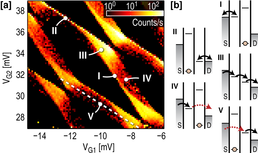
Figure 35(a) shows a charge stability diagram for the DQD, measured by counting electrons tunneling into and out of the DQD. The data was taken with a bias voltage of applied across the DQD, giving rise to finite-bias triangles of sequential transport [65]. The diagrams in Fig. 35(b) show schematics of the DQD energy levels for different positions in the charge stability diagram. Depending on energy level alignment, different kinds of electron tunneling are possible.
At the position marked by I in Fig. 35(a), the electrochemical potential of QD1 is aligned with the Fermi level of the source lead. The tunneling is due to equilibrium fluctuations between source and QD1. A measurement of the count rate as a function of provides a way to determine both the tunneling rate and the electron temperature in the source lead [20]. The situation is reversed at point II in Fig. 35(a). Here, electron tunneling occurs between QD2 and the drain, thus giving an independent measurement of and the electron temperature of the drain lead. At point III within the triangle of Fig. 35(a), the levels of both QD1 and QD2 are within the bias window and the tunneling is due to sequential transport of electrons from the source lead into QD1, over to QD2 and finally out to the drain. The electron flow is unidirectional and the count rate relates directly to the current flowing through the system [22]. Between the triangles, there are broad, band-shaped regions with low but non-zero count rates where sequential transport is expected to be suppressed due to Coulomb blockade [cases IV and V in Fig. 35(a,b)]. The finite count rate in this region is attributed to electron tunneling involving virtual processes. These features will be investigated in more detail in the forthcoming sections.
To begin with, we use the time-resolved charge detection methods to characterize the system. Typical time traces of the QPC current for DQD configurations marked by I and II in Fig. 35(a) are shown in Fig. 36(a). The QPC current switches between two levels, corresponding to electrons entering or leaving QD1 (case I) or QD2 (case II). The change as one electron enters the DQD is larger for charge fluctuations in QD2 than in QD1. This reflects the stronger coupling between the QPC and QD2 due to the geometry of the device. A measurement of thus gives information about the charge localization in the DQD.
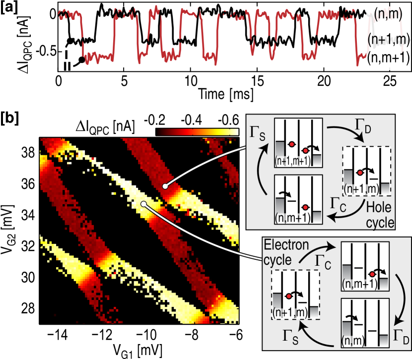
In Fig. 36(b) we investigate the charge localization in more detail by plotting the absolute change in QPC current for the same set of data as in Fig. 35(a). The detector essentially only measures two different values of ; either or . Comparing the results of Fig. 36(b) with the sketches in Fig. 35(b), we see that regions with high match with the regions where we expect the counts to be due to electron tunneling in QD2, while the regions with low come from electron tunneling in QD1.
The regions inside the bias triangles are described in detail in the energy level diagrams of Fig. 36(b). We assume each QD to hold n and m electrons, respectively. In the lower triangle, the current is carried by a sequential electron cycle. Starting from the (n,m)-configuration, an electron will tunnel in from the source lead at a rate making the transition . The electron then passes on to QD2 at a rate before leaving to drain at the rate . Since the rate is much faster than the detector bandwidth (and ), the detector will only register transitions between the two states and . Therefore, we expect the step height within the lower triangle to be equal to measured for electron fluctuations in QD2, in agreement with the results of Fig. 36.
For the upper triangle, the DQD holds an additional electron and the current is carried by a hole cycle. Starting with both QDs occupied , an electron in QD2 may leave to the drain , followed by a fast interdot transition from QD1 to QD2 . Finally, an electron can tunnel into QD1 from the source lead . In the hole cycle, the detector is not able to resolve the time the system stays in the state; the measurement will only register transitions between and . This corresponds to fluctuations of charge in QD1, giving the low value of in Fig. 36(b). Finally, we note that at the transition between regions of low and high the electron wavefunction delocalizes onto both QDs. This provides a method for determining the interdot coupling energy , which is the subject of the next section.
4.2 Determining the coupling energy
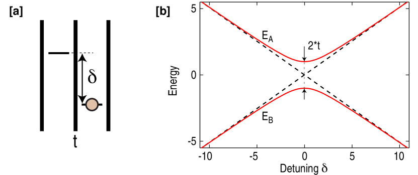
In the previous section we have shown that interdot transitions occur much faster than the detector bandwidth, but so far we did not try to quantify the tunnel coupling. As already mentioned, the coupling can be determined by looking at the delocalization of charge as a function of energy separation of the QD states [18]. To simplify the problem, we consider the DQD as a tunnel-coupled two-level system containing one electron, isolated from the environment [see Fig. 37(a)]. We introduce the basis states describing the electron sitting on the left or the right QD, respectively. The two states are tunnel coupled with coupling and separated in energy by the detuning . The Hamiltonian of the system is
| (81) |
The eigenvectors of the Hamiltonian in Eq. (81) form the bonding and antibonding states of the system. The eigenvalues give the energies , of the two states, with
| (82) |
The energies are plotted in Fig. 37(b); at zero detuning, the states anticross due to the coupling energy. For a finite temperature , the system will be in a statistical mixture of the bonding and antibonding states. The occupation probabilities and of the two states are determined by detailed balance,
| (83) |
In the measurement, we use the change of the QPC current () when one electron enters the DQD to determine the amount of charge localized in the individual QDs. To evaluate this quantity from Eqs. (81-4.2), we take the thermal population of the bonding and antibonding states and project them onto the states and
| (84) | |||||
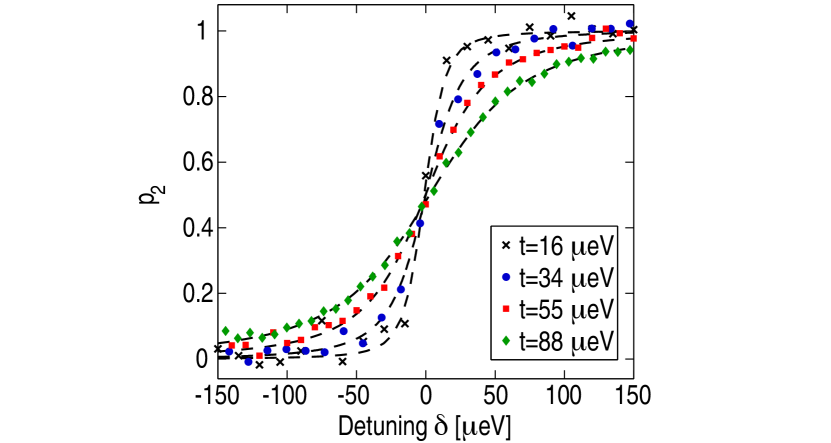
Next, we compare the results of Eq. (4.2) with experimental data. Figure 38 shows the measured electron population on QD2 versus detuning, extracted from the change in QPC current . The signal has been normalized to the levels measured for complete localization in QD1 and QD2. The different data sets are taken for different gate voltages, demonstrating the possibility to tune the tunnel coupling. The dashed lines are fits to Eq. (4.2), showing good agreement with the data. It should be noted that this method for determining the tunneling coupling can only be used as long as the coupling is larger than the thermal broadening. For a temperature of , the limit corresponds to .
4.3 Cotunneling
We now focus on the regions of weak tunneling occuring in regions outside the boundaries expected from sequential transport. In case IV, the electrochemical potential of QD1 is within the bias window, but the potential of QD2 is shifted below the Fermi level of the source and not available for transport. We attribute the non-zero count rate for this configuration to be due to electrons cotunneling from QD1 to the drain lead. The time-energy uncertainty principle still allows electrons to tunnel from QD1 to drain by means of a higher order process. In case V, the situation is analogous but the roles of the two QDs are reversed; electrons cotunnel from the source into QD2 and leave sequentially to the drain lead.
To investigate the phenomenon more carefully, we measure the rates for electrons tunneling into and out of the DQD in a configuration similar to the configuration along the dashed line in Fig. 35(a). The line corresponds to keeping the electrochemical potential of QD2 fixed within the bias window and sweeping . The data is presented in Fig. 39. In the region marked by A in Fig. 39, electrons tunnel sequentially from source into QD1, relax from QD1 down to QD2 and finally tunnel out from QD2 to the drain lead. Proceeding from region A to region B, the electrochemical potential is lowered so that an electron eventually gets trapped in QD1. At point B, the electrons lack an energy to leave to QD2. Still, electron tunneling is possible by means of a virtual process [67]. Due to the energy-time uncertainty principle, there is a time-window of length within which tunneling from QD1 to QD2 followed by tunneling from the source into QD1 is possible without violating energy conservation. An analogous process is possible involving the next unoccupied state of QD1, occuring on timescales , where and is the charging energy of QD1. The two processes correspond to electron cotunneling from the source lead to QD2. Continuing from point B to point C, the unoccupied state of QD2 is shifted into the bias window and electron transport is again sequential.
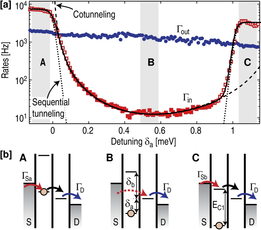
In the sequential regime (regions A and C), we fit the rate for electrons entering the DQD to a model involving only sequential tunneling [dotted lines in Fig. 39(a)] [19]. The fit allows us to determine the tunnel couplings between source and the occupied ()/unoccupied () states of QD2, giving , and . Going towards region B, the rates due to sequential tunneling are expected to drop exponentially as the energy difference between the levels in QD1 and QD2 is increased. In the measurement, the rate initially decreases with detuning, but the decrease is slower than exponential and flattens out as the detuning gets larger. This is in strong disagreement with the behavior expected for sequential tunneling. Instead, in a region around point B we attribute the measured rate to be due to electrons cotunneling from source to QD2.
The rate for cotunneling from source to QD2 is given as [68]:
| (85) |
Here, , are the tunnel couplings between the occupied/unoccupied states in QD1 and the state in QD2. The first term describes cotunneling involving the occupied state of QD1, the second term describes the cotunneling over the unoccupied state and the third term accounts for possible interference between the two. The phase defines the phase difference between the two processes. To determine one needs to be able to tune the phases experimentally, which is not possible from the measurement shown in Fig. 39(a). In the following we therefore assume the two processes to be independent (). Interference effects between cotunneling processes have been studied in detail in Ref. [69].
The dashed line in Fig. 39(a) shows the results of Eq. (85), with fitting parameters and . These values are in good agreement with values obtained from charge localization measurements. The values for and are taken from measurements in the sequential regimes. We emphasize that Eq. (85) is valid only if and if sequential transport is sufficiently suppressed. The data points used in the fitting procedure are marked by filled squares in the figure. It should be noted that the sequential tunneling in region C prevents investigation of the cotunneling rate at small . This can easily be overcome by inverting the DQD bias. The rate for electrons tunneling out of the DQD [ in Fig. 39(a)] shows only slight variations over the region of interest. This is expected since stays constant over the sweep. The slight decay of with increased detuning comes from tuning of the tunnel barrier between QD2 and the drain [28].
The cotunneling may be modified by the existence of a near-by QPC. If the QPC were able to detect the presence electron in QD2 during the cotunneling we would expect this to influence the cotunneling process. For the measurements in Fig. 39(a) the QPC current was kept below 10 nA. This gives an average time delay between two electrons passing the QPC of . Since this is larger than the typical cotunneling time, it is unlikely that the electrons in the QPC are capable of detecting the cotunneling process. The influence of the QPC may become important for larger QPC currents. However, when the QPC bias voltage is larger than the detuning (), the fluctuations in the QPC current may start to drive inelastic charge transitions between the QDs [12, 69]. Such transitions will compete with the cotunneling. For this reason it was not possible to extract what effect the presence of the QPC may have on the cotunneling process.
4.4 Molecular states
The overall good agreement between Eq. (85) and the measured data demonstrates that time-resolved charge detection techniques provide a direct way of quantitatively using the time-energy uncertainty principle. However, a difficulty arises as ; the cotunneling rate in Eq. (85) diverges, as visualized for the dashed line in Fig. 39(a). The problem with Eq. (85) is that it only takes second-order tunneling processes into account. For small detuning the cotunneling described in Eq. (85) must be extended to include higher order processes [70].
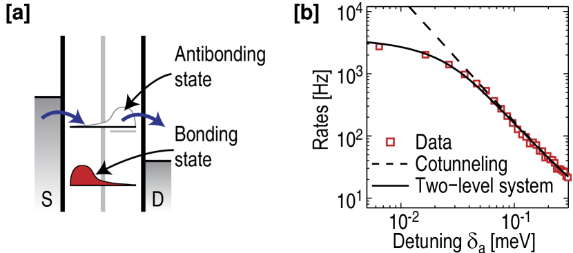
A different approach is to assume the coupling between the QDs to be fully coherent and describe the DQD in terms of the bonding and antibonding molecular states [71, 72]. Both the sequential tunneling and the cotunneling can then be treated as first-order tunneling processes into the molecular states; what we in Fig. 39 referred to as cotunneling would be tunneling into an antibonding state. The model is sketched in Fig. 40(a). The bonding state is occupied and in Coulomb blockade. Still, an electron may tunnel from drain into the antibonding state. Due to the large detuning, the antibonding state is mainly located on QD2, the overlap with the electrons in the source lead is small and the tunneling is weak. Changing the detuning will have the effect of changing the shape of the molecular states and shift their weights between the two QDs.
To calculate the rate for electrons tunneling from source into the antibonding molecular state of the DQD as visualized in Fig. 40(a), we use the formalism from section 4.2 and project the thermal population , of the molecular states and onto the unperturbed state of QD1, . This gives the probability of finding an electron in QD1 if making a projective measurement in the -basis. The measured rate is equal to the probability of finding QD1 being empty multiplied with , the tunneling rate between the source and the unperturbed state in QD1.
| (86) | |||||
For large detuning, the bonding and antibonding states are well localized in QD1 and QD2, respectively. Here, we should recover the results for the cotunneling rate obtained for the second-order process [Eq. (85)]. First, we assume low temperature , so that the electron only populates the bonding ground state ( and ):
| (87) |
In the limit the relation reduces to and the rate approaches the result of the second-order cotunneling processes in Eq. (85). The advantage of the molecular-state model is that it is valid for any detuning, both in the sequential and in the cotunneling regime.
The solid line in Fig. 39(a) shows the results of Eq. (86). The equation has been evaluated twice, once for the occupied [(n,m)] and once for the unoccupied state in QD2 [(n,m+1)]; the curve in Fig. 39(a) is the sum of the two rates. The same parameters were used as for the cotunneling fit of Eq. (85). The model shows very good agreement with data over the full range of the measurement. To compare the results of the molecular-state and the cotunneling model in the regime of small detuning, we plot the data in Fig. 39(a) on a log-log scale [Fig. 40(b)]. For large detuning, the tunneling rate follows the predicted by both the molecular-state and the cotunneling model. For small detuning, the deviations become apparent as the cotunneling model diverges whereas the molecular-state model still reproduces the data well.
4.5 Excited states
So far, we have only considered cotunneling involving the ground states of the two QDs. The situation is more complex if we include excited states in the model; the measured rate may come from a combination of cotunneling processes involving different QD states. To investigate the influence of excited states experimentally, we start by extracting the DQD excitation spectrum using finite bias spectroscopy [65]. If the coupling between the QDs is weak (, with being the mean level spacing in each QD), the DQD spectrum essentially consists of the combined excitation spectrum of the individual QDs. For a more strongly coupled DQD the QD states residing in different dots will hybridize and delocalize over both QDs. In this section we consider a relatively weakly coupled configuration () and assume the excited states to be predominantly located within the individual QDs.
Figure 41 shows a magnification of two triangles from Fig. 35(a), measured with both negative and positive bias applied across the DQD. Excited states are visible within the triangles, especially for the case of positive bias [marked with arrows in Fig. 41(a)]. Transitions between excited states occur along parallel lines at which the potential of QD1 is held constant; this indicates that the excited states are located in QD1. To investigate the states more carefully, we measure the separate tunneling rates and along the dashed lines in Fig. 41. The results are presented in Fig. 42, together with a few sketches depicting the energy level configuration of the system.
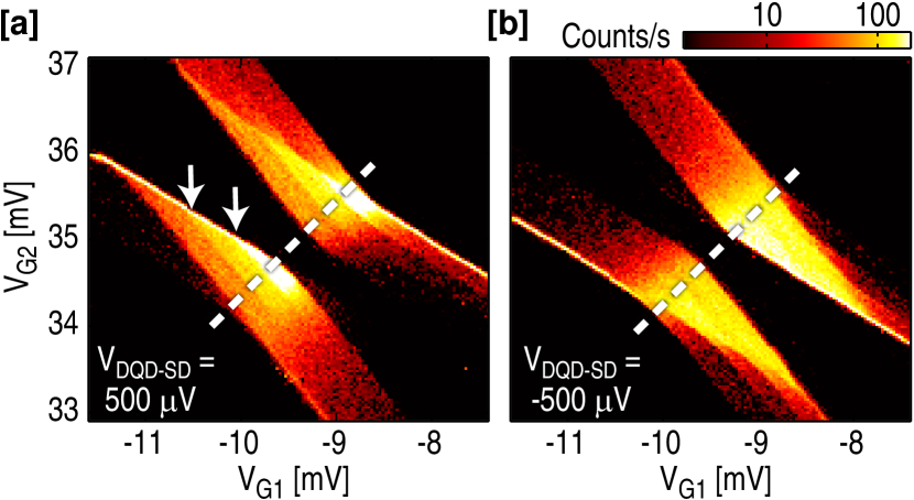
We begin with the results for the positive bias case, which are plotted in Fig. 42(a). Going along the dashed line in Fig. 41(a) corresponds to keeping the detuning between the QDs fixed and shifting the total DQD energy. The measurements were performed with a small detuning () to ensure that electron transport is unidirectional. Because of this, the outermost parts of the traces in Fig. 42(a) correspond to regions where transport is due to cotunneling [compare the dashed line with the position of the triangle in Fig. 41(a)]; the regions where transport is sequential are shaded gray in Fig. 42(a).
Starting in the regime marked by I in Fig. 42(a,c), electrons may tunnel from source into the ground state of QD1, relax down to QD2 and tunnel out to the drain lead. Assuming the relaxation process to be much faster than the other processes, the measured rates and are related to the tunnel couplings of the source and drain and . Going to higher gate voltages lowers the overall energy of both QDs. At the position marked by an arrow in Fig. 42(a), there is a sharp increase in the rate for tunneling into the DQD. We attribute this to the existence of an excited state in QD1; as shown in case II in Fig. 42(c), the electron tunneling from source into QD1 may enter either into the ground or the excited state , giving an increase in . When further lowering the DQD energy another excited state comes into the bias window and increases even more [second arrow in Fig. 42(a)]. The rate for tunneling out of the DQD shows only minor variations within the region of interest. This supports the assumption that the excited states quickly relax and that the electron tunnels out of the DQD from the ground state of QD2
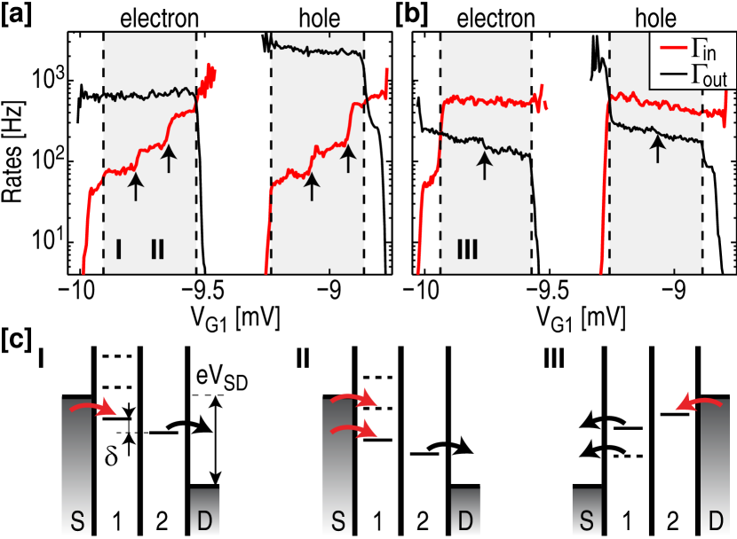
Finally, continuing to the edge of the shaded region (), the potential of QD2 goes below the Fermi level of the drain. Here, electrons get trapped in QD2 and the tunneling-out rate drops drastically. At the same time, increases; when the electron in QD2 eventually tunnels out, the DQD may be refilled from either the source or the drain lead. The picture described above is repeated in the triangle with hole transport (). This is expected, since the hole transport cycle involves the same QD states as in the electron case. An interesting feature is that shows essentially the same values in both the electron and the hole cycle, while increases by a factor of three. The presence of the additional electron in QD1 apparently affects the tunnel barrier between drain and QD2 more than an additional electron in QD2 affects the barrier between QD1 and source.
Next, we move over to the case of negative bias [Fig. 42(b)]. Here, the roles of QD1 and QD2 are inverted, meaning that electrons enter the DQD into QD2 and leave from QD1. Following the data and the arguments presented for the case of positive bias, one would expect this configuration to be suitable for detecting excited states in QD2. However, looking at the tunneling rates within the sequential region of Fig. 42(b), the rate for entering QD2 () stays fairly constant, while the rate for tunneling out decreases at the point marked by the arrow. Again, we attribute the behavior to the existence of an excited state in QD1.
The situation is described in sketch III of Fig. 42(c). The electrochemical potential of QD1 is high enough to allow the electron in the -state to tunnel out to the source and leave the DQD in an excited state . Since the energy difference is smaller than , the transition involving the excited state appears below the ground state transition. As the overall DQD potential is lowered, the transition energy involving the excited state goes below the Fermi level of the drain, resulting in a drop of as only the ground state transition is left available. Similar to the single QD case [20], the tunneling-in rate samples the excitation spectrum for the (n+1,m)-configuration, while the tunneling-out rate reflects the excitation spectrum of the -DQD.
To conclude the results of Fig. 42, we find two excited states in QD1 in the configuration with and , and one excited state in QD1 in the configuration, with . No clear excited state is visible in QD2. This does not necessarily mean that such states do not exist; if they are weakly coupled to the lead they will only have a minor influence on the measured tunneling rates. Excited states in both QDs have been measured in other configurations; there, we find similar spectra of excited states for both QDs.
4.6 Inelastic cotunneling
Next, we investigate the cotunneling process in the presence of excited states. Looking carefully at the lower-right regions of the negative-bias triangles in Fig. 41(b), we see that the count rates in the cotunneling regions outside the triangles are not constant along lines of fixed detuning (corresponds to going in a direction parallel to the dashed line). Instead, the cotunneling regions seem to split into three parallel bands.
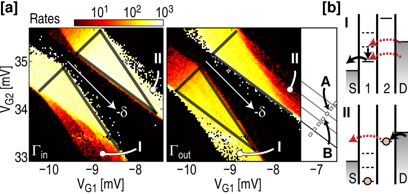
In Fig. 43(a), we plot the tunneling rates and for electrons entering and leaving the DQD, extracted from the same set of data as used in Fig. 41(b). The thick solid lines mark the edges of the finite-bias triangles. Again, the cotunneling rates outside the triangles are not uniform; parallel bands appear in for the position marked by I and in for the position marked by II in the figures.
To understand the data we draw energy level diagrams for the two configurations [see Fig. 43(b)]. Focusing first on case I, we see that the electrochemical potential of QD1 is within the bias window, whereas QD2 is detuned and in Coulomb blockade. The cotunneling occurs via QD2 states; electrons cotunnel from drain into QD1, followed by sequential tunneling from QD1 to the source lead. The picture is in agreement with what is measured in Fig. 43(a); the cotunneling rate () is low and strongly depends on detuning , while the sequential rate is high and essentially independent of detuning. The three bands seen in occur because of the excited states in QD1; depending on the average DQD energy, electrons may cotunnel from drain into one of the excited states, relax to the ground state and then leave to the source lead. The state of QD2 remains unaffected by the cotunneling process. For this configuration, we speak of elastic cotunneling.
The situation is different in case II. Here, cotunneling occurs in QD1 as electrons tunnel directly from QD2 into the source lead. This means that is sequential while describe the cotunneling process. As in case I, the cotunneling rate splits up into three bands; we attribute this to cotunneling where the state of QD1 is changed during the process. QD1 ends up in one of its excited states. The energy of the electron arriving in the source lead is correspondingly decreased compared to the electrochemical potential of QD2. Here, the cotunneling is inelastic.
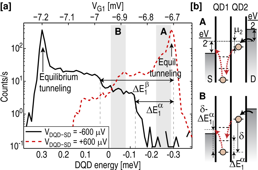
The inelastic cotunneling is described in greater detail in Fig. 44. In Fig. 44(a) we plot the count rate for positive and negative DQD bias, measured along the dashed line at the right edge of Fig. 43(a). Figure 44(b) shows energy level diagrams for negative bias at two positions along this line. The bias voltage is applied symmetrically to the DQD, meaning that the Fermi levels in source and drain leads are shifted by relative to the Fermi energy at zero bias [dotted line in Fig. 44(b)]. In the measurement of Fig. 44(a) we sweep the average DQD energy while keeping the detuning constant. The average DQD energy is defined to be zero when aligns with the zero-bias Fermi energy in the leads [i.e. when ].
Starting in the configuration marked by A, cotunneling is only possible involving the QD2 ground state. Cotunneling is weak, with count rates being well below 1 count/s. Continuing to case B, we raise the average DQD energy. When the electrochemical potential of QD2 is sufficiently increased compared to the Fermi level of the source, inelastic cotunneling becomes possible leading to a sharp increase in count rate. The process is sketched in Fig. 44(b); it involves the simultaneous tunneling of an electron from QD2 to the first excited state of QD1 with an electron in the QD1 ground state leaving to the source. The process is only possible if
| (88) |
Here, is the energy of the first excited state in QD1. The position of the step in Fig. 44(a) directly gives the energy of the first excited state, and we find .
Further increasing the average DQD energy makes an inelastic process involving the second excited state in QD2 possible, giving . Finally, as the DQD energy is raised to become equal to half the applied bias, the electrochemical potential of QD2 aligns with Fermi level of the drain lead. Here electron tunneling mainly occurs due to equilibrium fluctuations between drain and QD2, giving a sharp peak in the count rate. The excited states energies extracted from the inelastic cotunneling give the same values as obtained from finite-bias spectroscopy within the triangles, as described in the previous section. The good agreement between the two measurements demonstrates the consistency of the model.
The dashed line in Fig. 44(a) shows data taken with reversed DQD bias; for this configuration the Fermi levels of the source and drain leads are inverted, the electrons cotunnel from source to QD2 and the peak due to equilibrium tunneling occurs at .
4.7 Noise in the cotunneling regime
Using time-resolved charge detection methods, we can extract the noise of electron transport in the cotunneling regime. For a weakly-coupled single QD in the regime of sequential tunneling, transport in most configurations is well-described by independent tunneling events for electrons entering and leaving the QD [40]. The Fano factor becomes a function of the tunneling rates [36]:
| (89) |
with . For symmetric barriers (), the Fano factor is reduced to 0.5 because of an increase in electron correlation due to Coulomb blockade. In the case of cotunneling, the situation is more complex. As described in the previous section, cotunneling may involve processes leaving either QD in an excited state. The excited state has a finite lifetime ; during this time, the tunneling rates may be different compared to the ground-state configuration [73]. We therefore expect that the existence of an electron in an excited state may induce temporal correlations on time scales on the order of between subsequent cotunneling events. In this way, the noise of the cotunneling current has been proposed as a tool to probe excited states and relaxation processes in QDs [74, 75].
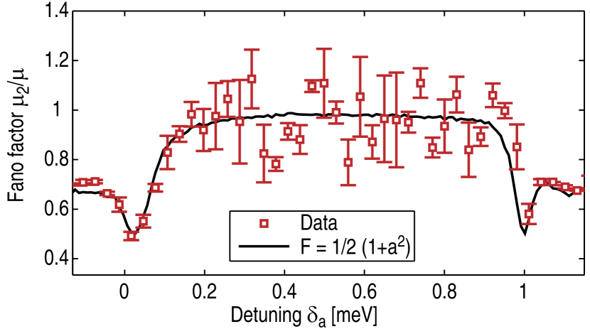
In Fig. 45, we plot the Fano factor measured from the same region as that of Fig. 39. The Fano factor was extracted by measuring the distribution function for transmitted charge through the system [40]. The solid line shows the result of Eq. (89), with tunneling rates extracted from the measured traces. In the outermost regions of the graph, the electrons tunnel sequentially through the DQD. Here, the Fano factor is reduced due to Coulomb blockade, similar to the single QD case. At the edges of the cotunneling regions, the Fano factor drops further down to . This is because the injection rate drops drastically as sequential transport becomes unavailable, while stays approximately constant. At some point we get , which means that the asymmetry is zero and the Fano factor of Eq. (89) shows a minimum. Further into the cotunneling region, the Fano factor approaches one as transport essentially becomes limited by a single rate; the cotunneling rate () is two orders of magnitude smaller than the sequential rate .
We do not see any major deviation from the results of Eq. (89), which is only valid assuming independent tunneling events. We have performed similar measurements in several inelastic and elastic cotunneling regimes, without detecting any clear deviations from Eq. (89). As it turns out, there are two effects that make it hard to detect correlations due to the internal QD relaxations. For the first, the correlation time is essentially set by the relaxation time , which typically occurs on a timescale. This is several orders of magnitude smaller than a typical tunneling time of [26]. Secondly, the slow cotunneling rate limits the amount of experimental data available within a reasonable measurement time. This explains the large spread between the data points in Fig. 45 in the cotunneling regime. We conclude that the measurement bandwidth currently limits the possibility of examining correlations in the cotunneling regime using time-resolved detection techniques. A higher-bandwidth detector would solve both the above mentioned problems. It would allow a general increase in the tunneling rates in the system, which would both decrease the difference between and as well as provide faster acquisition of sufficient statistics.
4.8 Spin effects in many-electron dots
So far, we have neglected the spin properties of the electrons by considering them to be spin-less particles. In few-electron double quantum dots, spin effects have been shown to lead to Pauli spin blockade [76, 77]; the current is strongly suppressed in configurations where a spin flip is required for electrons to traverse the DQD. The Pauli blockade configuration has been utilized for performing electron spin resonance experiments [78, 79] as well as for studying interactions between the electron and nuclei spin systems [80, 77, 81, 82].
In the system investigated here, the DQD contains a relatively large number of electrons; from the energy scales and from the geometry of the device we estimate each QD to hold electrons. This makes the observation of spin blockade more difficult, since neither the excitation spectrum nor the exact QD spin configuration is well known. For few-electron QDs, the first two electrons fill up spin-degenerate single-particle states and form a spin-pair [83]. Spin pairing has also been reported in many-electron chaotic dots [31] and quantum rings [84]. If spin-pairing occurs, it is possible to get a spin-zero many-electron ground state and we may neglect the spin-less core of electrons and only consider the spin of the outermost electrons [81].
To investigate the occurrence of spin pairing and spin blockade in our device, we use the methods of section 2.7 to determine the degeneracy of the QD ground states. Depending on the occupancy of a spin-degenerate state, the rates for electrons tunneling into and out of a QD should differ by a factor of two. By performing such measurements for consecutive electron filling in the DQDs, we can extract a possible spin configuration of the DQD. The method is visualized in Fig. 46, together with a possible spin configuration for the hexagons from Fig. 35(a). The numbers in the figure do not refer to the absolute DQD electron population but to the number of excess electrons relative to the configuration indicated by (0,0).
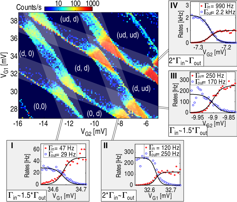
Starting in the Coulomb-blockaded region marked by (0,0), we increase the gate voltage to add an electron into QD2. At the transition to (0,d) (case I in Fig. 2.7), we find that the tunneling rate for electrons entering QD2 is larger than the rate for electrons tunneling out. Increasing the gate voltage further to add another electron to QD2 (case II), the relation between and is reversed. This is in agreement with successive filling of electrons into a degenerate state; if both degenerate states are initially unoccupied (case I), an incoming electron may tunnel into either state with an effective tunneling rate . Here, is the degeneracy factor and is the tunnel coupling to the lead. On the other hand, the rate for electrons leaving the QD is determined by the number of occupied degenerate states. With only one electron in the QD we get and thus expect . The situation is reversed if the QD is initially occupied (case II); here we expect .
If we assume the degeneracy to be due to spin states, the data indicates that QD2 is successively filled up with one spin-down and one spin-up electron. The pattern is repeated if we perform similar measurements for QD1 (cases III-IV). From these measurements we extract the spin configurations shown in Fig. 46. It should be noted that the degeneracy factors in cases I and III are lower than the factor expected from spin-degenerate states. This might be due to changes in the tunneling coupling within the gate voltage region of interest, although the coupling normally only changes slightly within the small voltage range used here (see section 2.6). Therefore, the spin configurations marked in Fig. 46 should not be considered as definite; we can not rule out other explanations for the data.
Keeping this reservation in mind but still assuming the spin configuration of Fig. 46 to be correct, we expect spin blockade to occur in the transport triangle involving the configurations (0,d), (d,d) and (0,ud). The principle of the blockade is explained in Fig. 47(a). We start in the configuration (0,d), where QD1 is empty and QD2 contains one excess electron. An electron may tunnel from source into QD1 and since the QD is initially empty, the incoming electron may be either spin-up or spin-down. If the spin is opposite to the spin of the electron in QD2, the electron in QD1 can continue to QD2 to form the spin singlet ground state (0,ud). Finally, an electron may leave to the drain which takes the system back to the state (0,d) and the cycle can be repeated.
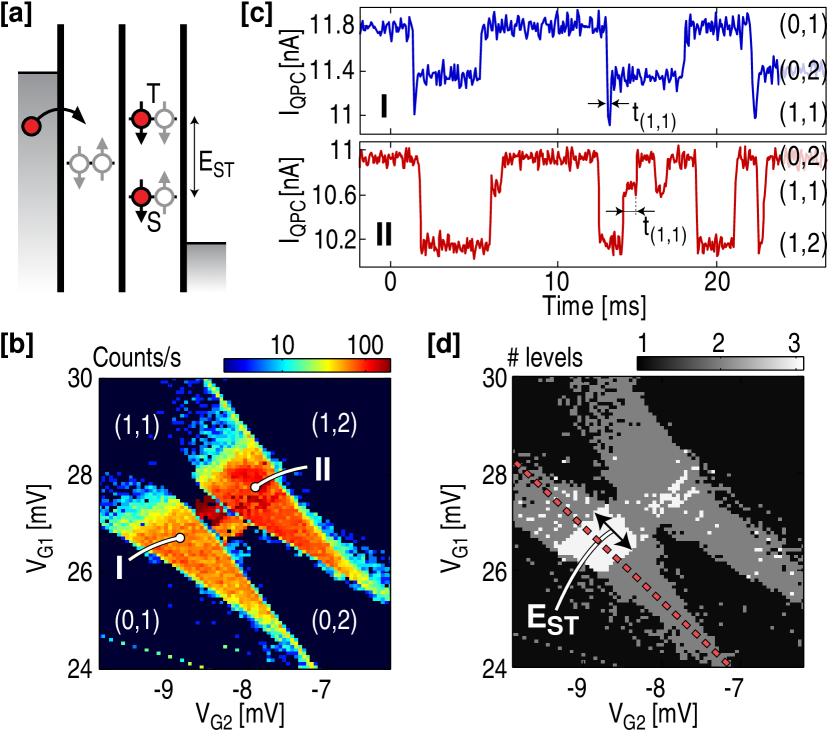
However, if the electron tunneling from source into QD1 has the same spin orientation as the electron in QD2, it cannot continue from QD1 to QD2. This is because of the singlet-triplet splitting in QD2; due to the exchange energy the system favors the formation of a spin singlet and the energy of the spin triplet is raised by the single-triplet splitting . The electron in QD1 is thus blocked until a spin-flip occurs in either QD1 and QD2. Since spin relaxation is slow, the effect leads to a sharp decrease in the current through the DQD [76]. In our case, we do not measure the average current but rather count the electrons as they pass through the structure. As mentioned in section 4.2, the tunnel coupling between the QDs is too strong to allow interdot charge transitions to be resolved in time. However, in the spin-blockade regime interdot charge transition from QD1 to QD2 should be limited by the spin relaxation rate, which for GaAs QDs has been reported to be several milliseconds or even seconds for magnetic fields of [55, 56]. This is within the bandwidth of the charge detector and we thus expect spin blockade to help make the interdot charge transitions resolvable.
Figure 47(b) shows the finite-bias charge stability diagram measured by counting electrons in the regime located between the (d,d) and (0,ud)-region of Fig. 46. The data shows two triangle-shaped regions of electron and hole transport expected from the applied voltage bias. Figure 47(c) shows examples of QPC current traces taken at the two positions marked in Fig. 47(b). Taking a closer look at the data from position I, we see that the time trace actually contains three levels; starting at the QPC current level labeled (0,1), the QPC current drops to level (1,1) as an electron tunnels into QD1. The electron relatively quickly continues to QD2 [level (0,2) in Fig. 47(c)], before tunneling out to the drain and taking the QPC conductance back to level (0,1). The ability of the QPC to determine if the electron is sitting in QD1 or QD2 comes directly from the geometry of the device; the QPC is located closer to QD1.
For case II of Fig. 47(b,c), transport is governed by the hole process . As for the electron process in case I, the transition that possibly involves spin relaxation is the one where the electron hops from QD1 to QD2 []. The timescale of the interdot transitions is marked by in the traces of Fig. 47(c). From the above discussion, we expect to be long enough to be measurable as long as the DQD detuning is smaller than the singlet-triplet spacing, . If , the electron in QD1 may tunnel to QD2 regardless of the spin direction and we expect to resolve only two levels in the QPC conductance traces. This is visualized in Fig. 47(d), where we plot the number of current levels detected by an automatic level detection algorithm. Focusing first on the electron transport cycle, there is a region of three-level traces situated at the base of the triangle. In the model of spin-blockade, the width of the region in direction of detuning is equal to the singlet-triplet splitting in QD2, giving . For the hole cycle, the region showing three levels is less regular. However, this is actually an artifact due to imperfections of the level detection algorithm; for the electron cycle (case I), the third, fast level occurs below the other levels, which makes it relatively easy to detect. It is much harder to reliably detect a fast third level if it occurs in-between the two main levels as in the hole region (case II). Manual inspection of the traces confirms that the region of three-level traces indeed has the same extension for the hole as for the electron cycle.
To get more quantitative concerning the time scale of the transition and to investigate if it is really related to spin relaxation, we measure the average of as a function of detuning [dashed line in Fig. 47(d)] and magnetic field. The result is presented in Fig. 48(a). As mentioned in the previous paragraph, the third level is only visible in the region of . Figure 48(b) shows a cross section taken at . The time spent in the (1,1)-state is around at zero magnetic field, but decays rapidly with increased B-field and disappears below the time resolution of the detector as .
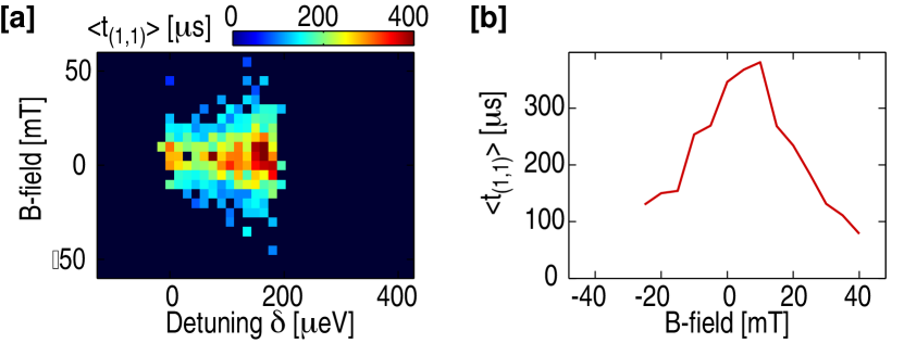
The spin blockade can be conveniently expressed using a model involving two-electron spin singlet (S) and triplet (T) states distributed over both QDs. In this language, the electron tunneling into the DQD from the source lead can enter either the singlet S(1,1) or the triplet T(1,1) state. The singlet S(1,1) quickly relaxes to S(0,2) followed by an electron leaving the DQD to the drain. On the other hand, if the electron enters into the triplet T(1,1), it can not proceed to T(0,2) since this state is raised by the singlet-triplet splitting in QD2. The triplet T(1,1) first needs to relax to S(1,1) before proceeding to S(0,2), leading to spin blockade.
For GaAs quantum dots, the spin blockade has been observed to be lifted at zero magnetic field because of mixing of the T(1,1) and S(1,1) states due to hyperfine interactions with the nuclear spin bath. The mixing energy is given by the magnitude of the random magnetic field generated by the fluctuating nuclear spins, with for a typical quantum dot containing nuclei. The mixing can be removed by applying an external magnetic field so that the electron Zeeman splitting becomes larger than the mixing energy . This typically occurs on a magnetic field scale of a few mT [77]. In our case, we observe the opposite behavior; the relaxation rate is minimal at zero magnetic field and increases with external magnetic field. In contrast to the setup of Ref. [77], we are in the strong coupling regime, with . As discussed in section 4.2, the tunnel coupling will hybridize the S(1,1) and S(0,2) singlet configurations and thereby keep the energy separation to the T(1,1) triplet larger than over the full range of detuning in Fig. 48(a). This suppresses the relaxation due to hyperfine mixing, even at zero external magnetic field [85].
A strong increase in the relaxation rate for small magnetic field has been seen in InAs DQD [81]. The behavior was attributed to the strong spin-orbit interactions of that material system. The main spin relaxation mechanism in few-electron single QDs in GaAs is also due to spin-orbit coupling, with relaxation rates increasing with external magnetic field [86, 56]. However, the relaxation times seen in Fig. 48(b) are much shorter and the B-field dependence much stronger than reported for few-electron single quantum dots. It is unclear how the existence of additional electrons in our DQD influences the relaxation process and it is uncertain if it is reasonable to assume electron-electron interactions to be weak enough to allow the QDs to be modeled using independent single-particle states. From the measurements presented here, one can not make a clear statement whether the observed features are due to spin relaxation or not. It would certainly be interesting to repeat the time-resolved measurements on a DQD containing only two electrons.
4.9 Weak interdot coupling
In the last part of this section, we treat the case where the three barriers of the DQD are tuned so that all tunneling processes occur on timescales slower than the bandwidth of the charge detector. In this regime it is possible to detect electrons tunneling back and forth between the QDs and thus determine the direction of the tunneling electrons [22].
It turned out to be difficult to reach this regime for the ring-shaped DQD of Fig. 33(a). The constrictions between the QDs were generally much more open than the constrictions to source and drain leads, which made it hard to pinch off the middle constriction while at the same time keeping source and drain open and forming well-defined dots. A measurement from one of the few cases where we were partly successful is shown in Fig. 49(a). The plot shows the charge stability diagram measured with bias applied across the DQD. The transport triangles due to electron and hole transport are well visible. There are a few striking things in this measurement compared to charge stability diagrams shown previously in this section. First, the size of the triangle due to hole transport is considerably smaller than the electron triangle. Although this is not quantitatively understood, we speculate that it is due to a weakly coupled state in QD2 that blocks transport in parts of the triangles. Second, there are bands of weak tunneling occurring outside the triangles. We attribute this to photon absorption processes driven by the current flowing in the QPC; this is the subject of section 5. Finally, there are stripes occurring parallel to the base line of the triangles; these are excited states in the QDs probed by interdot transitions.
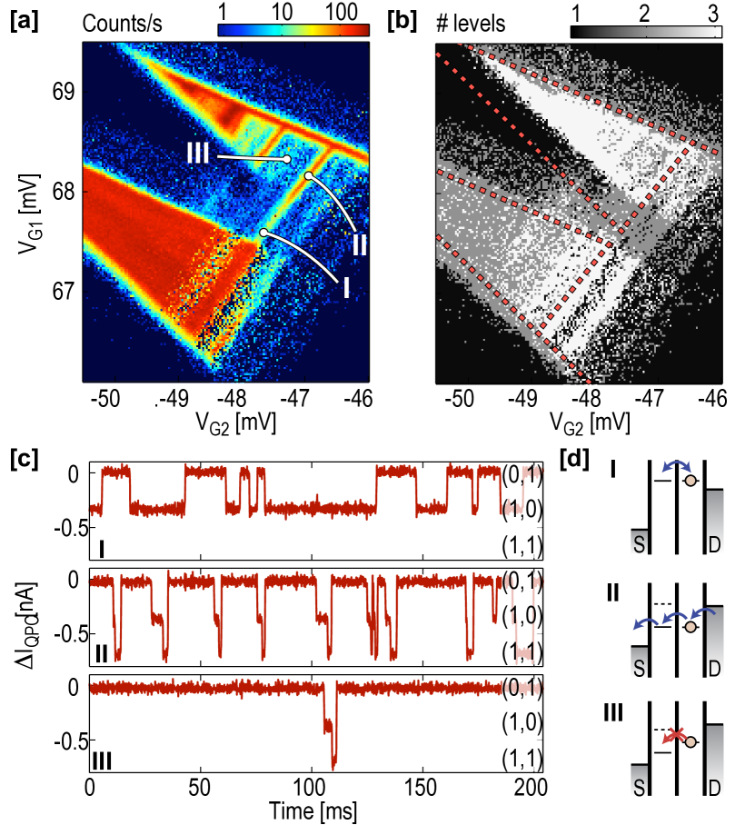
Figure 49(b) shows the number of QPC current levels found with the automatic level detection algorithm. Three levels are found in most of the hole transport triangle as well as in large parts of the electron transport triangle, showing that tunneling between the QDs is indeed slow enough to be detected by the detector. Figure 49(c) shows three QPC conductance traces taken at the positions marked in Fig. 49(a). Energy level diagrams for the corresponding configurations are shown in Fig. 49(d).
Starting at the position marked by I, the two QD levels are aligned but shifted outside the bias window. Here, equilibrium fluctuations occur between the QDs. The QPC conductance trace shows transitions between two levels corresponding to an electron sitting on QD1 and QD2, respectively. The transitions occur on a relatively slow timescale of .
Continuing to case II, we keep the alignment of the levels in the two QDs but shift them inside the bias window of the hole transport cycle. Looking at the trace in Fig. 49(c), we see that the transition of electrons from QD2 to QD1 [] still occurs on a timescale comparable to case I. However, before the electron in QD1 has time to tunnel back to QD2, an electron is quickly refilled into QD2 from the drain lead and takes the QPC conductance to the (1,1) level. Afterwards, an electron may leave from QD1 to source and the system is back in the (0,1) state. Each cycle corresponds to one electron being transferred through the DQD.
The timescale for interdot transition is clearly slower than the tunneling involving the source or drain lead. The DQD current is thus limited by the central barrier. This is clearly visualized if we continue to case III, which corresponds to a slightly lowered electrochemical potential of QD1 relative to QD2. Here, the interdot transition can not occur resonantly; the tunneling electron needs to lose parts of it energy to the environment. This makes the tunneling process less probable and reduces the count rate in the region of case III in Fig. 49(a). The QPC conductance trace Fig. 49(c) shows that the electron indeed spends most of the time in QD2; once a transition to QD1 occurs it is immediately followed by tunneling from drain to QD2 and from QD1 to source, as discussed for case II. Finally, by further lowering the electrochemical potential of QD1 an excited state of QD1 lines up with QD2 and tunneling may again occur resonantly. This is the reason for the stripes parallel to the triangle baseline occurring inside the triangles.
The above discussion raises a few interesting questions concerning the interdot tunneling. First, what sets the width of the regime with resonant interdot tunneling? In case I, the electrons in the DQD are isolated from the leads and it seems unlikely that the DQD transitions should be influenced by the thermal distribution of the electrons in the leads. Second, what are the relaxation processes leading to the slow but non-zero tunneling rates in the non-resonant regime? To answer the first question, we take the data from Fig. 49(a) and use the known capacitive lever arms to convert the gate voltages into energy of the DQD. The result is presented in Fig. 50(a), where we plot the count rate for the hole transport triangle vs average DQD energy and detuning energy . The two axes have the same scaling, which makes it easier to compare energy scales of different processes.
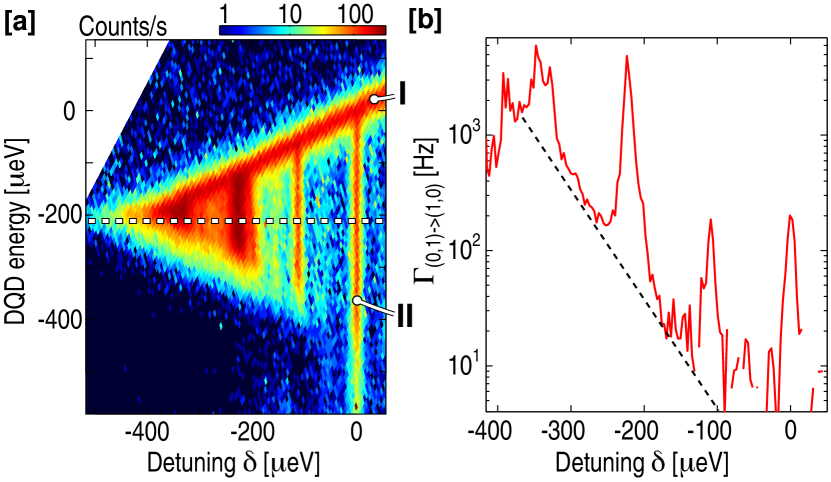
We first focus on the tilted line with slope marked by I in Fig. 50(a). The line is due to equilibrium fluctuations between QD1 and the source lead; the broadening of the line is a direct measure of the electron temperature in the source lead (see section 2.2). By converting the energy to temperature we find that the electron temperature in the lead is around . However, the width of the thermally-broadened line stands in sharp contrast to the narrow vertical lines coming from interdot transitions (case II). The width of these lines is only around a quarter of the thermal-broadened line, which would correspond to a temperature of . This energy scale matches relatively well to the base temperature of the cryostat. A possible explanation could therefore be that the broadening occurs because of scattering with thermally excited acoustic phonons. A straightforward experimental check of this hypothesis would be to investigate how the broadening changes when raising the base temperature of the cryostat. Unfortunately, shortly after measuring the data in Fig. 49 we had to warm up the cryostat, and we were not able to reach the same regime in subsequent cool-downs.
A different energy scale is given by the tunnel coupling between the two QDs. If we assume the transport between the QDs to be coherent and convert the measured tunneling rate of to a coupling energy, we find
| (90) |
This is obviously several orders of magnitudes smaller than the width measured in the experiment. Still, the discussion raises some interesting questions concerning coherence and projective measurements. For a fully coherent system, the electron wavefunctions in the two QDs hybridize and form bonding and antibonding states that delocalize over both dots. At zero detuning both the bonding and antibonding wavefunctions have the same spatial extent, which means that a charge detector would not be able to resolve transitions between the two states independently of how slowly the transitions occur. The very fact that we detect electrons tunneling back and forth between the QDs even at zero detuning is an obvious indication that the system is not coherent. The decoherence rate is faster than the tunnel coupling, meaning that the coherent evolution of an electron between the two QDs is interrupted by a projective measurement taking the electron back into the states of the individual QDs. The rate at which we observe transitions between the two QDs thus depends not only on the tunnel coupling but also on the decoherence in the system. It would certainly be interesting to perform measurements in a regime where the tunnel coupling and the decoherence rate are comparable, and to investigate how the measured transition rates are affected by the presence of the QPC and its ability to perform projective measurements. One would expect an increased QPC bias to introduce additional effects compared to the intrinsic decoherence.
Finally, we come back to the question of the relaxation mechanism leading to the finite count rate between the lines of resonant tunneling in Fig. 49(a) and Fig. 50(a). Figure 50(b) shows the interdot transition rate measured along the dashed line in Fig. 50(b), extracted from traces similar to the ones shown in Fig. 49(c). The ground state transition as well as transitions due to three exited states give rise to clear peaks in the figure. In between the peaks, the rate of the non-resonant transition increases strongly as the detuning gets larger.
Spontaneous energy relaxation in a DQD has been investigated previously using conventional current measurement techniques [87]. In that work, the authors find that the emission rate decreases with increased detuning and attribute the mechanism behind the relaxation to phonon emission. This is in disagreement with the results of Fig. 50(b), where the emission rate clearly increases with detuning. It would therefore be interesting to perform further experiments in this regime and investigate the inelastic tunneling of Fig. 50(b) in more detail. In addition to checking the obvious influence of the temperature of the phonon bath there could be other explanations for the relaxation such as photon emission to the nearby quantum point contact [88] or to anywhere else in the environment.
5 Detector back-action
In the previous sections, we used quantum point contacts to measure charge transitions in various mesoscopic structures. While doing so we assumed the point contact to be an idealized detector that does not exert any back-action on the measured object. In reality, this is not true. The scattering of electrons in the quantum point contact leads to emission of microwave radiation. In this section, we show that the radiation may drive transitions in a double quantum dot. Turning the perspectives around, the double quantum dot can be seen as a frequency-selective microwave detector. The frequency of the absorbed radiation is set by the energy separation between the levels in the dots, which is easily tuned with gate voltages. By combining this with time-resolved charge detection techniques, we can directly relate the detection of a tunneling electron to the absorption of a single photon.
5.1 Using the double quantum dot as a frequency-selective detector
The interplay between quantum optics and mesoscopic physics opens up new horizons for investigating radiation produced in nanoscale conductors [89, 90]. Microwave photons emitted from quantum conductors are predicted to show non-classical behavior such as anti-bunching [91] and entanglement [92]. Experimental investigations of such systems require sensitive, high-bandwidth detectors operating at microwave-frequency [93]. On-chip detection schemes, with the device and detector being strongly capacitively coupled, offer advantages in terms of sensitivity and large bandwidths. In previous work, the detection mechanism was implemented utilizing photon-assisted tunneling in a superconductor-insulator-superconductor junction [94, 51] or in a single quantum dot (QD) [52].
Aguado and Kouwenhoven proposed to use a double quantum dot (DQD) as a frequency-tunable quantum noise detector [88]. The idea is sketched in Fig. 51(a), showing the energy levels of the DQD together with a quantum point contact acting as a noise source. The DQD is operated with a fixed detuning between the electrochemical potentials of the left and right QDs. For an isolated system, the DQD is in the Coulomb blockade regime and there will be no current flowing. However, if the system absorbs an energy from the environment, the electron in QD1 is excited to QD2. This electron may leave to the drain lead, a new electron enters from the source contact and the cycle can be repeated. The process induces a current flow through the system. Since the detuning may be varied continuously by applying appropriate gate voltages, the absorption energy is tunable.
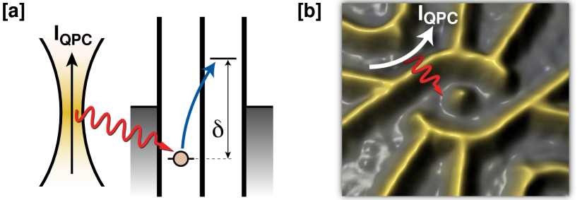
The scheme is experimentally challenging, due to low current levels and fast relaxation processes between the QDs [95]. Here, we show that these problems can be overcome by using time-resolved charge-detection techniques to detect single electrons tunneling into and out of the DQD. Apart from giving higher sensitivity than conventional current measurement techniques, the method also allows us to directly relate a single-electron tunneling event to the absorption of a single photon. The system can thus be viewed as a frequency-selective single-photon detector for microwave energies. This, together with the fact that the charge-detection methods allow precise determination of the device parameters, provide major advantages compared to other setups [90, 93, 94, 51, 52].
The measurements were performed on the structure shown in Fig. 51(b), which consists of two quantum dots embedded in a ring, together with a nearby QPC. As described in section 4, we tune the surrounding gates so that only the upper tunnel barrier connecting the two QDs is kept open. The tunnel coupling between the QDs was set to , as determined using charge localization measurements explained in section 4.2. The tunneling barriers between the DQD and the source and drain contacts were tuned to a few kHz to enable electron counting in real-time. In the following, we present measurements taken with zero bias across the DQD. Fig. 52(a) shows count rates close to the triple point where the , and states are degenerate [see inset of Fig. 52(a)]. The arguments presented below are applicable also for the triple point between the , , states, but for simplicity we consider only the first case. At the triple point [marked by a white dot in Fig. 52(a)], the detuning is zero and both dots are aligned with the Fermi level of the leads. The two strong, bright lines emerging from this point come from resonant tunneling between QD1 and the source lead (lower-right line) or between QD2 and the drain lead (upper-left line). The amplitude of the count rate at the lines gives directly the strength of the tunnel couplings to source and drain leads [6, 17], and we find the rates to be and .
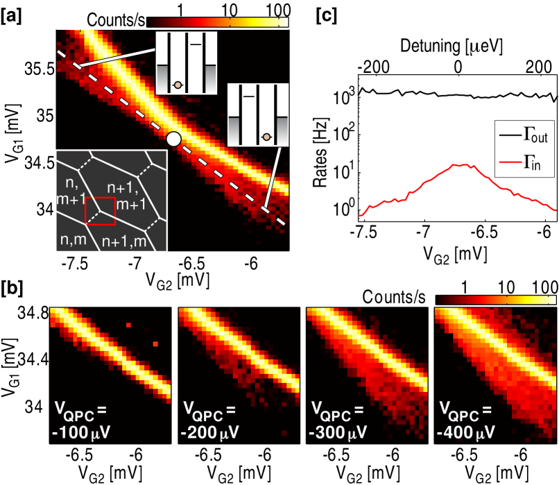
Along the white dashed line in Fig. 52(a), there are triangle-shaped regions with low but non-zero count rates where tunneling is expected to be strongly suppressed due to Coulomb blockade. The DQD level arrangements inside the triangles are shown in the insets. Comparing with the sketch in Fig. 51(a), we see that both regions have DQD configurations favorable for noise detection. The dashed line connecting the triangles is the detuning axis, with zero detuning occuring at the triple point. We define the detuning as , so that the detuning is negative in the upper-left part of the figure.
In Fig. 52(b), the lower-right part of Fig. 52(a) was measured for four different QPC bias voltages. The resonant line stays the same in all four measurements, but the triangle becomes both larger and more prominent as the QPC bias is increased. This is a strong indication that the tunneling is due to absorption of energy from the QPC. The counts observed above the resonance line for are due to electrons being excited from the ground state to the first excited state of the DQD.
The time-resolved measurement technique allows the rates for electron tunneling into and out of the DQD to be determined separately [40]. Figure 52(c) shows the rates and measured along the dashed line of Fig. 52(a). The rate for tunneling out stays almost constant along the line, but is maximum close to the triple point and falls of rapidly with increased detuning. This suggests that only the rate for electrons tunneling into the DQD is related to the absorption process. To explain the experimental findings we model the system using a rate-equation approach. For a configuration around the triple point, the DQD may hold , or electrons. We label the states , and and draw the energy diagrams together with possible transitions in Fig. 53(a). The figure shows the case for negative detuning, with . Note that when the DQD holds two excess electrons, the energy levels are raised by the mutual charging energy, .
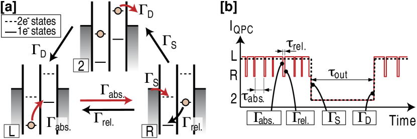
In Fig 53(b) we sketch the time evolution of the system. The red curve shows the expected charge detector signal assuming a detector bandwidth much larger than the transitions rates. Starting in state , the electron is trapped until it absorbs a photon and is excited to state (with rate ). From here, the electron may either relax back to state (rate ) or a new electron may enter QD1 from the source lead and put the system into state (rate ). Finally, if the DQD ends up in state , the only possible transition is for the electron in the right dot to leave to the drain lead.
The relaxation rate for a similar DQD system has been measured to be [96], which is much faster than the available measurement bandwidth. Therefore, the detector will not be able to register the transitions where the electron is repeatedly excited and relaxed between the dots. Only when a second electron enters from the source lead [transition marked by in Fig. 53(a, b)], the DQD will be trapped in state for a sufficiently long time () to allow detection. The measured time trace will only show two levels, as indicated by the dashed line in Fig. 53(b). Such a trace still allows extraction of the effective rates for electrons entering and leaving the DQD, and . To relate , to the internal DQD transitions, we write down the master equation for the occupation probabilities of the states:
| (91) |
Again, we assume negative detuning, with . The measured rates , are calculated from the steady-state solution of Eq. 91:
| (92) | |||||
| (93) |
In the limit , the first expression simplifies to
| (94) |
The corresponding expressions for positive detuning are found by interchanging and in Eqs. (91-94). Coming back to the experimental findings of Fig. 52(c), we note that only shows small variations within the region of interest. This together with the result of Eq. (93) suggest that we can take , to be independent of detuning. The rate in Eq. (94) thus reflects the dependence of on detuning. Assuming also to be constant, a measurement of gives directly the absorption spectrum of the DQD. The measurements cannot exclude that also varies with , but as we show below the model assuming independent of detuning fits the data well.
Equation (94) shows that the low-bandwidth detector can be used to measure the absorption spectrum, even in the presence of fast relaxation. Moreover, the detection of an electron entering the DQD implies that a quantum of energy was absorbed immediately before the electron was detected. The charge detector signal thus relates directly to the detection of a single photon. The efficiency of the detector is currently limited by the bandwidth of the charge detector. However, it should be possible to increase the bandwidth significantly by operating the QPC in a mode analogous to the radio-frequency single-electron transistor [97, 98, 11, 99].
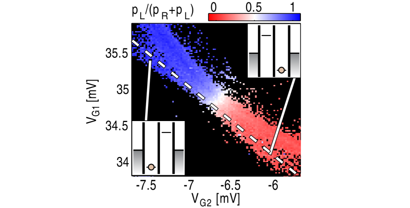
To justify the assumption , we note that even when the detector is too slow to detect individual transitions between the states and , its dc-response still gives the average population of the two states. In Fig. 54, we plot the relative population of state , , for the same gate voltage configuration as in Fig. 52(a). The data was extracted by analyzing the absolute change in the QPC conductance for one electron tunneling into DQD (see section 4.2). Looking at the region of negative detuning (upper-left part of Fig. 54), the average DQD population within the regions of photon-assisted tunneling is very close to the pure -state. The electron spends most of the time in QD1, which validates the assumption . Similar arguments can be applied for the region of positive detuning.
For fixed DQD detuning, the processes described above only pump electrons in one direction. The system may therefore thought of as a ratchet, giving unidirectional electron flow even at zero bias [95].
5.2 Measuring the QPC emission spectrum
In the following, we use the DQD to quantitatively investigate the microwave radiation emitted from the nearby QPC. Figure 55(a) shows the measured count rate for electrons leaving the DQD versus detuning and QPC bias. The data was taken along the dashed line of Fig. 52(a), with gate voltages converted into energy using lever arms extracted from finite bias measurements. Due to the tunnel coupling between the QDs, the energy level separation of the DQD is given by . The dashed lines in 55(a) show , with . A striking feature is that there are no counts in regions with . This originates from the fact that the voltage-biased QPC can only emit photons with energy [88, 52, 93]. The result presents another strong evidence that the absorbed photons originate from the QPC.
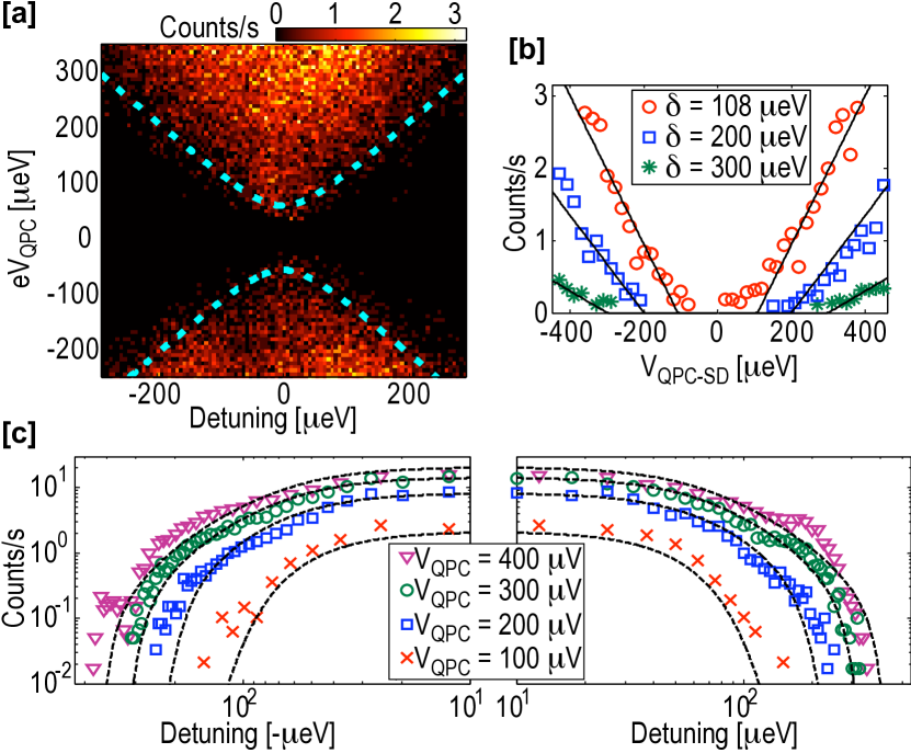
To describe the results quantitatively, we consider the emission spectrum of a voltage biased QPC with one conducting channel. In the low-temperature limit , the spectral noise density for the emission side () takes the form (see [88] for the full expression)
| (95) |
where is the transmission coefficient of the channel. Using the model of Ref. [88], we find the absorption rate of the DQD in the presence of the QPC:
| (96) |
The constant is the capacitive lever arm of the QPC on the DQD and is the zero-frequency impedance of the leads connecting the QPC to the voltage source. Equation (96) states how well fluctuations in the QPC couple to the DQD system.
Figure 55(b) shows the measured absorption rates versus , taken for three different values of . As expected from Eqs. (95, 96), the absorption rates increase linearly with bias voltage as soon as . The different slopes for the three data sets are due to the -dependence in the relation between the emission spectrum and the absorption rate of Eq. (96). In Fig. 55(c), we present measurements of the absorption spectrum for fixed . The rates decrease with increased detuning, with sharp cut-offs as . In the region of small detuning, the absorption rates saturate as the DQD level separation approaches the limit set by the tunnel coupling. The dashed lines show the combined results of Eqs. (94-96), with parameters , , , , , and . Using as a fitting parameter, we find . This should be seen as a rough estimate of due to uncertainties in , but it shows reasonable agreement with previously reported measurements [96]. The overall good agreement between the data and the electrostatic model of Eq. (96) supports the assumption that the interchange of energy between the QPC and the DQD is predominantly mediated by photons instead of phonons or plasmons.
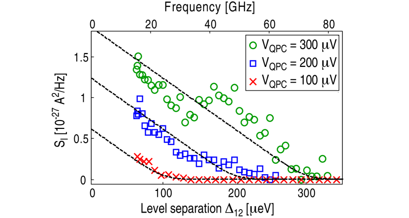
The data for shows some irregularities compared to theory, especially at large positive detuning. We speculate that the deviations are due to excited states of the individual QDs, with excitation energies smaller than the detuning. In Fig. 56, we convert the detuning to level separation and use Eq. (96) to extract the noise spectrum of the QPC. The linear dependence of the noise with respect to frequency corresponds well to the behavior expected from Eq. (95). Again, the deviations at are probably due to an excited state in one of the QDs. The excited states are also visible in finite-bias spectroscopy, giving a single-level spacing of . This sets an upper bound on frequencies that can be detected with the detector. The frequency-range can be extended by using DQD in carbon nanotubes [100] or InAs nanowires [101, 102], where the single-level spacing is significantly larger [5].
5.3 Finite DQD bias regime
Finally, we apply a voltage bias over the DQD in order to compare the tunneling originating from sequential transport with the tunneling due to photon absorption processes. Figure 57(a) shows a charge stability diagram measured with DQD bias . The two triangles associated with electron and hole transport cycles are clearly visible. Besides that, we have regions of cotunneling (see section 4.3) as well as sharp lines with tunneling due to equilibrium fluctuations whenever the electrochemical potential of QD1 or QD2 lines up with the Fermi levels in the source or drain, respectively. In addition, there are faint triangles appearing in the detuning direction opposite to the transport triangles; we attribute these features to photon-assisted tunneling (PAT).
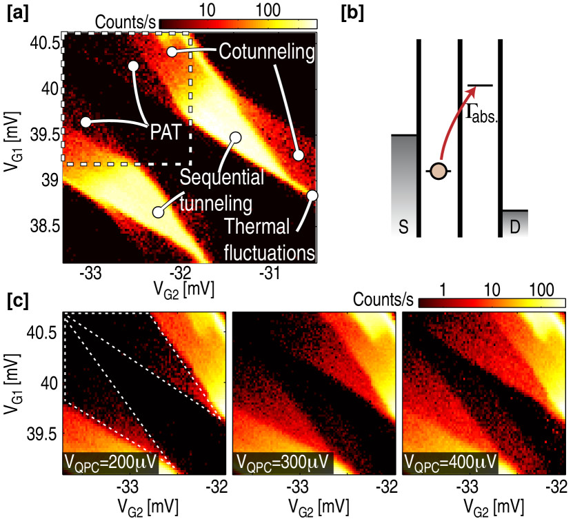
The DQD energy level configuration in the upper region with faint tunneling (next to the hole transport triangle) is depicted in Fig. 57(a). In this regime the DQD may hold one or two excess electrons. For this energy level alignment neither sequential tunneling nor cotunneling is possible. The DQD can only change its state if an electron in QD1 absorbs a photon and is excited to QD2. From this configuration, an electron may enter QD1 from the source lead followed by the electron in QD2 leaving to the drain. In Fig. 57(c), we present blow-ups of the region marked by the dashed rectangle in Fig. 57(a), measured for different QPC bias voltages. The dashed lines in the leftmost panel in Fig. 57(c) show the regions where we expect photon-assisted tunneling. As the QPC bias is increased, we see that the count rate inside these regions indeed goes up significantly. For the highest QPC bias voltage, there are extra features appearing outside the anticipated PAT-region. Again, we attribute this to an excited state in QD2.
6 Single-electron interference
A central concept of quantum mechanics is the wave-particle duality; matter exhibits both wave- and particle-like properties and can not be described by either formalism alone. Up to this point, we have treated the electrons as particles tunneling back and forth between quantum dots. In this chapter, we investigate their wave properties by studying interference of individual electrons taking two different paths in an Aharonov-Bohm interferometer. The time-resolved charge detection technique enables us to count electrons one-by-one as they pass the interferometer. In this way we make a direct measurement of the self-interference of a single electron. With increased bias voltage across the quantum point contact a back-action is exerted on the interferometer leading to dephasing. We attribute this to emission of radiation from the quantum point contact, which drives non-coherent electronic transitions in the quantum dots.
6.1 The Aharonov-Bohm effect
One of the cornerstone concepts of quantum mechanics is the superposition principle as demonstrated in the double-slit experiment [103]. The partial waves of individual particles passing a double slit interfere with each other. The ensemble average of many particles detected on a screen agrees with the interference pattern calculated using propagating waves [Fig. 58(a)]. This has been demonstrated for photons, electrons in vacuum [104, 105] as well as for more massive objects like -molecules [106]. The Aharonov-Bohm (AB) geometry provides an analogous experiment in solid-state systems [107]. Partial waves passing the arms of a ring acquire a phase difference due to a magnetic flux, enclosed by the two paths [Fig. 58(b)]. Here, we set out to perform the interference experiment by using a quantum point contact to detect single-electron tunneling in real-time.
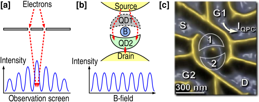
We first discuss the experimental conditions necessary for observing single-electron AB interference. We make use of a geometry containing two quantum dots within the AB-ring. Figure 58(c) shows the structure, with the two QDs (marked by 1 and 2) tunnel-coupled by two separate barriers. It is the same structure as investigated in chapters 4 and 5, but this time tuned to a regime where both barriers connecting the QDs are kept open. Following the sketch in Fig. 58(b), electrons are provided from the source lead, tunnel into QD1 and pass on to QD2 through either one of the two arms. Upon arriving in QD2, the electrons are detected in real-time by monitoring the conductance of the nearby QPC [4, 7, 6, 62]. Coulomb blockade prohibits more than one excess electron to populate the structure, implying that the first electron must leave to the drain before a new one can enter. This enables time-resolved operation of the charge detector and ensures that we measure interference due to individual electrons.
To avoid dephasing, the electrons should spend a time as short as possible on their way from source to QD2. This is achieved by raising the electrochemical potential of QD1 so that electrons in the source lead lack an energy required for entering QD1 [see Fig. 60(b)]. The time-energy uncertainty principle still allows electrons to tunnel from source to QD2 by means of second order processes. The tunneling process is then limited to a short time scale set by the uncertainty relation, with .
6.2 Experimental realization
In the experiment, we apply appropriate gate voltages to tune the tunneling rates between the double quantum dot (DQD) and the source and drain leads to values below . The tunneling coupling between the QDs is set to a few GHz, as determined from charge localization measurements (see section 4.2). Figure 59 shows the charge stability diagram of the DQD systems, measured by counting electrons entering and leaving the DQD within a fixed period of time. The data was taken with bias applied between source and drain. The hexagon pattern together with the triangles of electron transport appearing due to the applied bias are well-known characteristics of DQD systems (see chapter 4). Between the triangles, there are broad, band-shaped regions with low but non-zero count rates where sequential transport is suppressed due to Coulomb blockade. The finite count rate in this region is attributed to electron tunneling involving virtual processes, as described in section 4.3. In the following paragraph we quickly repeat the main results from that section.
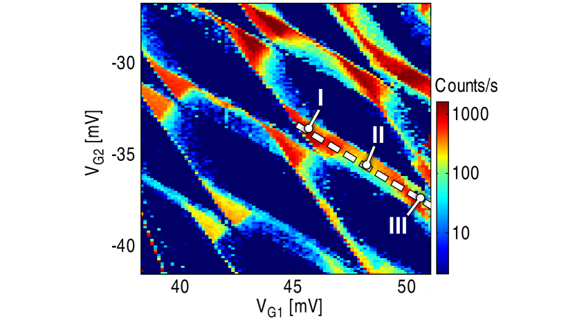
Figure 60(a) shows the rates for electrons tunneling into and out of the DQD measured along the dashed line in Fig. 59. Going along the dashed line corresponds to lowering the electrochemical potential of QD1 while keeping the potential of QD2 constant. In the region marked by I, electrons tunnel sequentially from the source into QD1, continue from QD1 to QD2 and finally leave QD2 to the drain lead. Proceeding to point II in Fig. 60(a), the electrochemical potential of QD1 is lowered and an electron eventually gets trapped in QD1 [see sketch in Fig. 60(b)]. At position II, the electron lacks an energy to leave to QD2. Due to the energy-time uncertainty principle, there is a time-window of length within which tunneling from QD1 to QD2 followed by tunneling from the source into QD1 is possible without violating energy conservation. An analogous process is possible involving the next unoccupied state of QD1, occuring on timescales . This corresponds to electron cotunneling from the source lead to QD2. By continuing to point III, the unoccupied state of QD1 is shifted into the bias window and electron transport is again sequential. The rate for electrons tunneling out of the DQD [, blue trace in Fig. 60(a)] shows only slight variations over the region of interest. This is expected, since the potential of QD2 stays constant along the dashed line in Fig. 59.
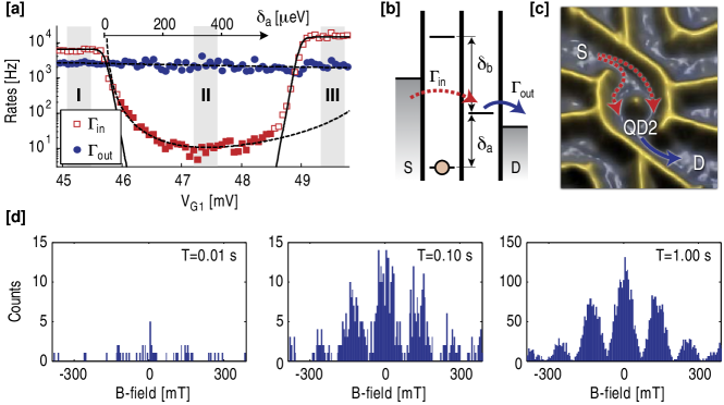
Coming back to the sketch of Fig. 58(b), we note that the cotunneling configuration of case II in Fig. 60(a,b) is ideal for investigating the Aharonov-Bohm effect for single electrons. Due to the low probability of the cotunneling process, the source lead provides low-frequency injection of single electrons into the DQD. The injected electrons cotunnel through QD1 into QD2 on a timescale much shorter than the decoherence time of the system, which is on the order of a few nanoseconds [108, 109]. This ensures that phase coherence is preserved. Finally, the electron stays in QD2 for a time long enough to be registered by the finite-bandwidth charge detector. The tunneling processes are sketched in Fig. 60(c).
Next, we tune the system to case II of Fig. 60(a) and count electrons as a function of magnetic field. Figure 60(d) shows snapshots taken at three different times. The electrons arriving in QD2 build up a well-pronounced interference pattern with period . This corresponds well to one flux quantum penetrating the area enclosed by the two paths. The visibility of the AB-oscillations is higher than , which is a remarkably large number demonstrating the high degree of phase coherence in the system. We attribute the high visibility to the short time available for the cotunneling process [110] and to strong suppression of electrons being backscattered in the reverse direction, which is otherwise present in AB-experiments. Another requirement for the high visibility is that the two tunnel barriers connecting the QDs are carefully symmetrized. The overall decay of the maxima of the AB-oscillation with increasing B is probably due to magnetic field effects on the orbital wavefunctions in QD1 and QD2.
In Fig. 61(a), we investigate the separate rates for electrons tunneling into and out of the DQD as a function of magnetic field. The y-axis corresponds to the dashed line in Fig. 59, i.e., to the energy of the states in QD1. The measurement shows a general shift of the DQD energy with the applied B-field, which we attribute to changes of the orbital wavefunctions in the individual QDs. Within the cotunneling region, shows well-defined B-periodic oscillations. At the same time, is essentially independent of the applied field. This is expected since measures the rate at which electrons leave QD2 to the drain, which occurs independently of the magnetic flux passing through the AB-ring [see Fig. 60(a,c)]. In Fig. 61(b), the bias over the DQD is reversed. This inverts the roles of and so that corresponds to the cotunneling process. Here shows B-periodic oscillations while remains unaffected. In the black regions seen in Fig. 61(b), no counts were registered within the measurement time of three seconds due to strong destructive interference for the tunneling-out process. As a consequence, it was not possible to determine in these regions.
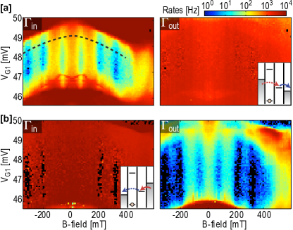
In the sequential regime (upper and lower parts of the color maps in Fig. 61), one would also expect AB-oscillations to occur. However, the effect would show up as a modulation of the coupling between the QDs (), which involves timescales of the order . The detection of single electron motion on such timescales is presently out of reach due to limited bandwidth of the detector.
6.3 Noise in the Aharonov-Bohm regime
In this section we investigate the noise of the current in the Aharonov-Bohm regime. Using the methods of chapter 3, we can extract the noise and the higher moments of the current distribution directly from the QPC conductance traces. Figure 62(a) shows a measurement of the current flowing through the DQD, measured in a regime close to the upper region of sequential tunneling in Fig. 61(a) [ at , dashed line in Fig. 61(a)]. When sweeping the magnetic field, we tune the voltages on gates G1 and G2 to compensate for the shift of the cotunneling region occurring due to orbital effects in the QDs. We chose to measure the AB-oscillation at relatively low DQD detuning; this enhances the cotunneling rates and allows us to collect more statistics within reasonable measurement times. On the other hand, it also increases the contribution of sequential tunneling and photon-assisted tunneling processes, giving the slightly lower visibility compared to Fig. 60(d). The small spikes seen at in Fig. 62(a) (marked by arrows) are attributed to single-QD excitations.
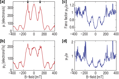
In Fig. 62(b), we plot the shot noise (second moment ) of the current distribution, extracted from the same set of data as used in Fig. 62(a). The noise curve shows strong similarities to the current trace in (a), with the AB-oscillations clearly visible. This is reasonable, since we expect the noise to scale with the magnitude of the current. In Fig. 62(c), we plot the Fano factor , extracted from the traces in Fig. 62(a,b). Also the Fano factor displays AB-oscillations, with a minimum occurring at (with ). We can understand this by considering the noise calculated for a single QD [see Eq. (50) in chapter 3]. There, we saw a reduction of the Fano factor due to Coulomb blockade, with the lowest noise given in a configuration where the tunneling rates for entering and leaving the QD were equal.
In the AB-regime, we also measure a current due to two tunneling rates; one is the cotunneling rate showing strong AB-oscillations (in this case ), while the other () is a sequential rate being independent of external magnetic field [compare the rates and in Fig. 61(a)]. At zero magnetic field, the cotunneling rate has a maximum and at this point it becomes comparable to the sequential rate . The two tunneling rates are relatively symmetric, giving a reduction of the Fano factor. For higher magnetic fields, the cotunneling rate drops drastically while stays constant. This results in a more asymmetric configuration and a Fano factor close to one.
In the region of higher magnetic fields the experimental precision of the measurement decreases. This is because of the low average count rate, giving less statistical data for extracting the moments compared to the region around . Finally, in Fig. 62(d) we plot , the generalized Fano factor for the third moment. This quantity also shows indications of AB-oscillations, but the experimental uncertainty in the high B-field range becomes even larger than for the conventional Fano factor.
6.4 Temperature effects
In Fig. 60(a), we investigate how the AB-oscillations are influenced by elevated temperatures. The dephasing of open QD systems is thought to be due to electron-electron interaction [111], giving dephasing rates that depend strongly on temperature [112]. Figure 63(a) shows the temperature dependence of the AB oscillations in our system. The amplitude of the oscillations remains almost unaffected up to , indicating that the coherence is not affected by temperature until the thermal energy becomes comparable to the single-level spacing of the QDs.
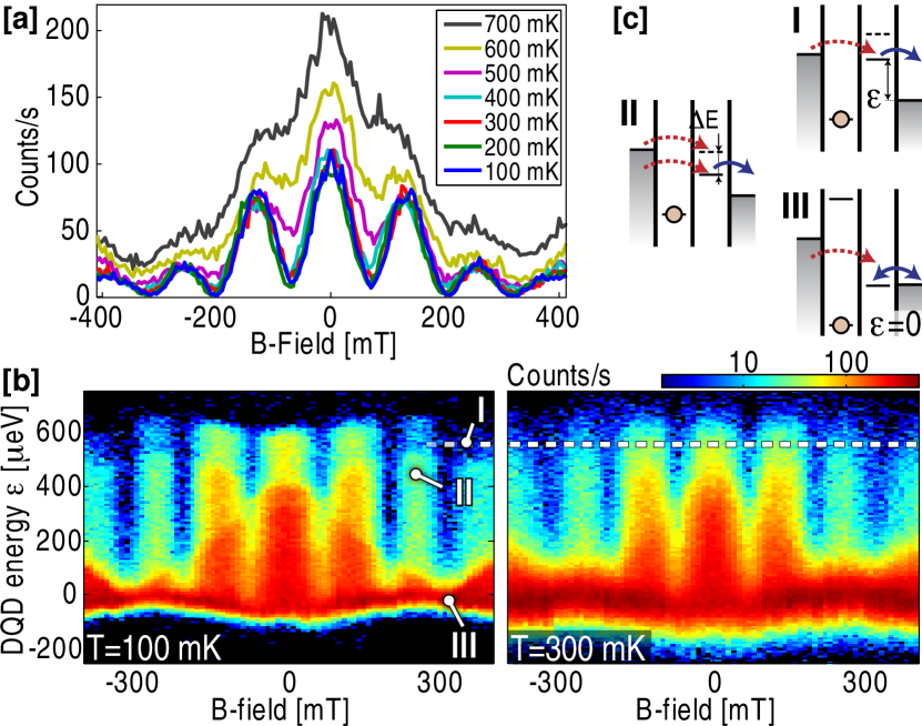
Figure 63(b) shows measurements of the electron count rate vs magnetic field and the average potential of the DQD, taken at and . Contrary to the measurements presented in Fig. 60 and Fig. 61, the potential difference between QD1 and QD2 is kept constant at while the overall DQD energy is shifted relative to the leads. The energy is taken to be zero when the level in QD2 is aligned with the Fermi level of the drain [case III in Fig. 63(b-c)]. Here, thermal population fluctuations tunneling between QD2 and the drain lead gives rise to a high count rate [strong red line in the lower part of Fig. 63(b)]. The width of the resonant line is set by the temperature of the electrons in the lead. Indeed, this line is clearly broader for the data.
Going to point I in Fig. 63(b,c), the energy of the DQD is raised compared to the leads and thermal fluctuation are no longer relevant. Here, electrons can only enter QD2 by cotunneling from the source lead. The data shows clear Aharanov-Bohm oscillations at both and , with comparable visibility. At the same time, the effect of the increased temperature is visible in the regime around . As the temperature is further increased, the line of thermal fluctuations becomes broader and eventually reaches the dashed line where the AB-oscillations of Fig. 63(a) were measured. This leads to the sharp decrease of the AB-visibility demonstrated in Fig. 63(a). We conclude that the decreased visibility at higher temperatures is due to an increase in thermal fluctuations of the DQD population.
6.5 Phase shifts for tunneling involving excited states
In the following, we investigate the phase of the AB-oscillations for different states in QD2. Previous experiments have shown phase shifts of occurring between consecutive Coulomb resonances in many-electron quantum dots [113, 114]. To measure AB-oscillations for consecutive electron fillings requires a relatively large shift of the gate voltages. Such measurements are difficult to perform in our setup, since large changes of gate voltages also affect the symmetry of the left and right arm connecting QD1 and QD2, which may strongly reduce the visibility of the AB-oscillations. Instead, we look at excited states of QD2 at fixed electron population [115].
In addition to highlighting temperature effects, the color map in Fig. 63(b) also shows the existence of excited states in the QDs. At point II in Fig. 63(b,c), the count rate is increased compared to case I. We attribute the increase to cotunneling into an excited state in QD2 (see section 4.6). Measuring the AB-oscillations at various DQD energy thus provides a way to investigate relative phases of the excited states in the QDs. From the data in Fig. 63(b), we see that the AB-oscillations persist in regions involving several excited states and that the phase of the oscillations seems to remain the same in all regions.
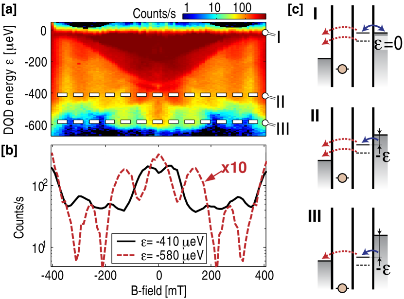
Depending on the direction of the applied bias, we can probe different excited states (see section 4.5). For positive bias, electrons cotunnel from source into QD2 and may thereby put QD2 into either the -electron ground state or an -electron excited state [see case II in Fig. 63(c)]. For negative DQD bias, the cotunneling involves an electron leaving from QD2 to the source contact. This involves transitions taking the QD2 into either its -electron ground state or into an -electron excited state. Since the energy difference is smaller than , the transition involving the excited state [] occurs at an energy below the ground state transition [see case II in Fig. 64(c)].
Figure 64(a) shows a measurement of the electron count rate versus magnetic field and DQD energy for negative DQD bias. Again, we define when the electrochemical potential of QD2 is aligned with the Fermi level of the drain lead [see case I in Fig. 64(c)]. Here, the tunneling is mainly due to equilibrium fluctuations between QD2 and the drain. As is reduced, the equilibrium fluctuations between QD2 and drain are no longer possible and electrons can only leave QD2 by cotunneling to the source. The cotunneling region shows AB-oscillations, but the oscillations are less uniform compared to the results for positive bias [Fig. 63(b)]. Between the position marked by II and III in Fig. 64(a), both the intensity and the behavior of the count rate changes drastically. In Fig. 64(b), we plot two cross sections from Fig. 64(a), taken at the positions of the dashed lines. Both traces show AB-oscillations, and both curves are symmetric around as expected from the Onsager relations. However, by comparing the positions of the maxima for we see that the phase is shifted by between the two curves. The reason for the apparent lack of phase rigidity is not understood, further measurements are needed for a more complete understanding of the phenomena.
Starting at point III in Fig. 64(a,c), the transition involving the []-electron excited state is below the Fermi level of the source so that only cotunneling through the ground state is possible. The trace in Fig. 64(b) belonging to point III is qualitatively similar to the data shown in Fig. 63(a), with both curves having a maximum appearing at . The similarity is expected, since both measurements involve cotunneling through the ground state of QD2. Moving to point II, the energy of the DQD is raised and the transition involving the excited state may also contribute to transport. The cotunneling rate measured in this regime is a sum of the processes involving the ground state and the excited state. However, since the rates at point II are almost an order of magnitude larger compared to point III, the behavior is to a large extent dominated by cotunneling from the excited state.
From this, we conclude that there is a phase shift occurring in the Aharonov-Bohm signal between tunneling involving the -electron ground state and a -electron excited state of QD2. Our findings are in agreement with previously reported results [113, 114, 115], but more measurements are needed to map out the complete phase behavior of the QD spectrum.
6.6 Decoherence due to the quantum point contact
In the experiment, we use the current in the QPC to detect the charge distribution in the DQD. In principle, the QPC could also determine whether an electron passed through the left or the right arm of the ring, thus acting as a which-path detector [117, 118]. If the QPC were to detect the electron passing in one of the arms, the interference pattern should disappear. In Fig. 65(a), we show the visibility of the AB-oscillations as a function of bias on the QPC. The visibility remains unaffected up to , but drops for higher bias voltages.
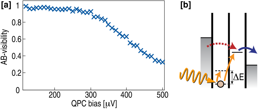
We argue that the reduced visibility is not due to which-path detection. At , the current through the QPC is . This gives an average time delay between two electrons passing the QPC of . Since this time is larger than the typical cotunneling time, it is unlikely that the electrons in the QPC are capable of performing an effective which-path measurement. Instead, we attribute the decrease of the AB-visibility to processes where the DQD absorbs photons emitted from the QPC. As described in chapter 5, such processes may indeed excite an electron from one QD to the other, as long as the energy of the excited state is lower than the energy provided by the QPC bias [12]. The radiation of the QPC may also drive transitions inside the individual QDs, thus putting one of the dots into an excited state [52]. A few possible absorption processes are sketched in Fig. 60(b).
As long as the QPC bias is lower than both the DQD detuning () and the single-level spacing of the individual QDs (), the AB visibility in Fig. 60(b) is close to unity. When raising the QPC bias above , we start exciting the individual QDs. With increased QPC bias, more states become available and the absorption process becomes more efficient. This introduces new virtual paths for the cotunneling process. Since the different paths may interfere destructively, the interference pattern is eventually washed out. In this way, the QPC has a physical back-action on the measurement which is different from informational back-action [119] and which-path detection previously investigated [117, 118].
7 Conclusions
In conclusion, we have measured current fluctuations in a semiconductor quantum dot, using a quantum point contact to detect single electron tunneling through the dot. We show experimentally the reduction of the second and third moment of the distribution when the quantum dot is symmetrically coupled to the leads. The setup can be used as a high-precision current meter for measuring ultra-low currents, with resolution several orders of magnitude better than that of conventional current meters.
The quantum point contact does not only serve as a charge detector, but also causes a back-action onto the measured device. Electron scattering in the quantum point contact leads to emission of microwave radiation, which may drive charge transitions in the quantum dot. Turning the perspective around, we show that a double quantum dot can be used as a frequency-selective detector for microwave radiation emitted from mesoscopic structures.
In addition, we demonstrate interference of single electrons in a solid state environment. Such experiments have previously been limited to photons or massive particles in a high-vacuum environment in order to decouple the degrees of freedom as much as possible from the environment. Our experiments demonstrate the exquisite control of modern semiconductor nanostructures which enables interference experiment at the level of single quasi-particles in a solid state environment. Once extended to include spin degrees of freedom [46] such experiments have the potential to facilitate entanglement detection [120, 47] or investigate the interference of particles [121] originating from different sources.
Financial support from the Swiss Science Foundation (Schweizerischer Nationalfonds) via NCCR Nanoscience and from the EU Human Potential Program financed via the Bundesministerium für Bildung und Wissenschaft is gratefully acknowledged.
Appendix A Cumulants or central moments of a distribution
The full distribution function or the complete set of central moments give a complete description of the current in a system. The moments and the distribution function contain the same information, making the two equivalent. Another way to represent the same information is in terms of the cumulants and the cumulant generating function . The cumulants are defined as [122]
| (97) |
with the cumulant generating function given by
| (98) |
In terms of the central moments, we have for the first few cumulants
| (99) |
The cumulants can be seen as an irreducible representation of the moments. Again, this means that the knowledge of either the moments , the cumulants or the distribution function provide the same information.
References
- [1] B. J. van Wees, H. van Houten, C. W. J. Beenakker, J. G. Williamson, L. P. Kouwenhoven, D. van der Marel, and C. T. Foxon. Quantized conductance of point contacts in a two-dimensional electron gas. Phys. Rev. Lett., 60(9):848, 1988.
- [2] D. A. Wharam, T. J. Thornton, R. Newbury, M. Pepper, H. Ahmed, J. E. F. Frost, D. G. Hasko, D. C. Peacock, D. A. Ritchie, and G A C Jones. One-dimensional transport and the quantisation of the ballistic resistance. Journal of Physics C, 21(8):209, 1988.
- [3] I. Shorubalko, R. Leturcq, A. Pfund, D. Tyndall, R. Krischek, S. Schön, and K. Ensslin. Self-aligned charge read-out for inas nanowire quantum dots. Nano Letters, 8(2):382–385, 2008.
- [4] M. Field, C. G. Smith, M. Pepper, D. A. Ritchie, J. E. F. Frost, G. A. C. Jones, and D. G. Hasko. Measurements of coulomb blockade with a noninvasive voltage probe. Phys. Rev. Lett., 70(9):1311, 1993.
- [5] S. Gustavsson, I. Shorubalko, R. Leturcq, T. Ihn, K. Ensslin, and S. Schön. Detecting terahertz current fluctuations in a quantum point contact using a nanowire quantum dot. Phys. Rev. B, 78:035324, 2008.
- [6] R. Schleser, E. Ruh, T. Ihn, K. Ensslin, D. C. Driscoll, and A. C. Gossard. Time-resolved detection of individual electrons in a quantum dot. Appl. Phys. Lett., 85(11):2005, 2004.
- [7] L. M. K. Vandersypen, J. M. Elzerman, R. N. Schouten, L. H. Willems van Beveren, R. Hanson, and L. P. Kouwenhoven. Real-time detection of single-electron tunneling using a quantum point contact. Appl. Phys. Lett., 85(19):4394, 2004.
- [8] S. Gustavsson. Time-resolved single-electron detection in semiconductor nanostructures. PhD thesis, ETH Zurich, 2008. Diss. ETH No. 17709.
- [9] S. W. Jung, T. Fujisawa, Y. Hirayama, and Y. H. Jeong. Background charge fluctuation in a GaAs quantum dot device. Appl. Phys. Lett., 85(05):768, 2004.
- [10] C. E. Shannon. A mathematical theory of communication. Bell System Technical Journal, 27:379, 1948.
- [11] D. J. Reilly, C. M. Marcus, M. P. Hanson, and A. C. Gossard. Fast single-charge sensing with a rf quantum point contact. Appl. Phys. Lett., 91:162101, 2007.
- [12] S. Gustavsson, M. Studer, R. Leturcq, T. Ihn, K. Ensslin, D. C. Driscoll, and A. C. Gossard. Frequency-selective single-photon detection using a double quantum dot. Phys. Rev. Lett., 99:206804, 2007.
- [13] S. Gustavsson, I. Shorubalko, R. Leturcq, S. Schön, and K. Ensslin. Measuring current by counting electrons in a nanowire quantum dot. Appl. Phys. Lett., 92(15):152101, 2008.
- [14] A. E. Gildemeister, T. Ihn, R. Schleser, K. Ensslin, D. C. Driscoll, and A. C. Gossard. Imaging a coupled quantum dot-quantum point contact system. J. Appl. Phys., 102(8):083703, 2007.
- [15] R. Held, S. Lüscher, T. Heinzel, K. Ensslin, and W. Wegscheider. Fabricating tunable semiconductor devices with an atomic force microscope. Appl. Phys. Lett., 75(8):1134, 1999.
- [16] A. Fuhrer, A. Dorn, S. Lüscher, T. Heinzel, K. Ensslin, W. Wegscheider, and M. Bichler. Invited Review Electronic properties of nanostructures defined in Ga[Al]As heterostructures by local oxidation. Superl. and Microstruc., 31(1):19–42, 1 January 2002.
- [17] O. Naaman and J. Aumentado. Poisson transition rates from time-domain measurements with finite bandwidth. Phys. Rev. Lett., 96:100201, 2006.
- [18] L. DiCarlo, H. J. Lynch, A. C. Johnson, L. I. Childress, K. Crockett, C. M. Marcus, M. P. Hanson, and A. C. Gossard. Differential charge sensing and charge delocalization in a tunable double quantum dot. Phys. Rev. Lett., 92:226801, 2004.
- [19] Leo P. Kouwenhoven, Charles M. Marcus, Paul M. McEuen, Seigo Tarucha, Robert M. Westervelt, and Ned S. Wingreen. Electron transport in quantum dots. In L. L. Sohn, L. P. Kouwenhoven, and G. Schön, editors, Mesoscopic Electron Transport, NATO ASI Ser. E 345, pages 105–214. Kluwer, Dordrecht, 1997.
- [20] S. Gustavsson, R. Leturcq, B. Simovic, R. Schleser, P. Studerus, T. Ihn, K. Ensslin, D. C. Driscoll, and A. C. Gossard. Counting statistics and super-poissonian noise in a quantum dot: Time-resolved measurements of electron transport. Phys. Rev. B, 74:195305, 2006.
- [21] Jonas Bylander, Tim Duty, and Per Delsing. Current measurement by real-time counting of single electrons. Nature, 434(7031):361–364, March 2005.
- [22] Toshimasa Fujisawa, Toshiaki Hayashi, Ritsuya Tomita, and Yoshiro Hirayama. Bidirectional counting of single electrons. Science, 312:1634, 2006.
- [23] R. Hanson, L. H. Willems van Beveren, I.T. Wink, J. M. Elzerman, W. J. M. Naber, F. H. L Koppens, L. P. Kouwenhoven, and L. M. K. Vandersypen. Single-shot readout of electron spin states in a quantum dot using spin-dependent tunnel rates. Phys. Rev. Lett., 94:196802, 2005.
- [24] M. Ciorga, A. Wensauer, M. Pioro-Ladriere, M. Korkusinski, J. Kyriakidis, A. S. Sachrajda, and P. Hawrylak. Collapse of the spin-singlet phase in quantum dots. Phys. Rev. Lett., 88:256804, 2002.
- [25] T. Inoshita and H. Sakaki. Electron relaxation in a quantum dot: Significance of multiphonon processes. Phys. Rev. B, 46:7260, 1992.
- [26] Toshimasa Fujisawa, David Guy Austing, Yasuhiro Tokura, Yoshiro Hirayama, and Seigo Tarucha. Allowed and forbidden transitions in artificial hydrogen and helium atoms. Nature, 419(6904):278, September 2002.
- [27] A. Bertoni, M. Rontani, G. Goldoni, and E. Molinari. Reduced electron relaxation rate in multi-electron quantum dots. Phys. Rev. Lett., 95:066806, 2005.
- [28] K. MacLean, S. Amasha, Iuliana P. Radu, D. M. Zumbühl, M. A. Kastner, M. P. Hanson, and A. C. Gossard. Energy-dependent tunneling in a quantum dot. Phys. Rev. Lett., 98(3):036802, 2007.
- [29] J. C. Chen, Zhenghua An, T. Ueda, S. Komiyama, K. Hirakawa, and V. Antonov. Metastable excited states of a closed quantum dot probed by an aluminum single-electron transistor. Phys. Rev. B, 74:045321, 2006.
- [30] S. Gustavsson, R. Leturcq, T. Ihn, K. Ensslin, D. C. Driscoll, and A. C. Gossard. Noise measurements in quantum dots using charge detection techniques. Physica E, 40:103, 2007.
- [31] S. Lüscher, T. Heinzel, K. Ensslin, W. Wegscheider, and M. Bichler. Signatures of spin pairing in chaotic quantum dots. Phys. Rev. Lett., 86(10):2118–2121, 2001.
- [32] R. de Picciotto, M. Reznikov, M. Heiblum, V. Umansky, G. Bunin, and D. Mahalu. Direct observation of a fractional charge. Nature, 389:162, 1997.
- [33] L. Saminadayar, D. C. Glattli, Y. Jin, and B. Etienne. Observation of the e/3 Fractionally Charged Laughlin Quasiparticle. Phys. Rev. Lett., 79(13):2526–2529, 1997.
- [34] X. Jehl, M. Sanquer, R. Calemczuk, and D. Mailly. Detection of doubled shot noise in short normal-metal/ superconductor junctions. Nature, 405:50–53, 2000.
- [35] Ya M Blanter and M Büttiker. Shot noise in mesoscopic conductors. Physics Reports, 336:1, 2000.
- [36] J. H. Davies, P. Hyldgaard, S. Hershfield, and J. W. Wilkins. Classical theory for shot noise in resonant tunneling. Phys. Rev. B, 46:9620, 1992.
- [37] H. Birk, M. J. M. de Jong, and C. Schönenberger. Shot-Noise Suppression in the Single-Electron Tunneling Regime. Phys. Rev. Lett., 75(8):1610–1613, 1995.
- [38] A. Nauen, I. Hapke-Wurst, F. Hohls, U. Zeitler, R. J. Haug, and K. Pierz. Shot noise in self-assembled InAs quantum dots. Phys. Rev. B, 66(16):161303, 2002.
- [39] A. Nauen, F. Hohls, N. Maire, K. Pierz, and R. J. Haug. Shot noise in tunneling through a single quantum dot. Phys. Rev. B, 70(03):033305, 2004.
- [40] S Gustavsson, R Leturcq, B Simovic, R Schleser, T Ihn, P Studerus, K Ensslin, D C Driscoll, and A C Gossard. Counting statistics of single-electron transport in a quantum dot. Phys. Rev. Lett., 96:076605, 2006.
- [41] G. B. Lesovik. Excess quantum noise in 2d ballistic point contacts. JETP Lett., 49:592–594, 1989.
- [42] M. Büttiker. Scattering theory of thermal and excess noise in open conductors. Phys. Rev. Lett., 65(23):2901–2904, 1990.
- [43] Eugene V Sukhorukov, Guido Burkard, and Daniel Loss. Noise of a quantum-dot system in the cotunneling regime. Phys. Rev. B, 63:125315, 2001.
- [44] A. Cottet, W. Belzig, and C. Bruder. Positive cross-correlations due to dynamical channel-blockade in a three-terminal quantum dot. Phys. Rev. B, 70:115315, 2004.
- [45] W. Belzig. Full counting statistics of super-Poissonian shot noise in multilevel quantum dots. Phys. Rev. B, 71(16):161301(R), 5 April 2005.
- [46] Daniel Loss and Eugene V Sukhorukov. Probing entanglement and non-locality of electrons in a double-dot via transport and noise. Phys. Rev. Lett., 84:1035, 2000.
- [47] Daniel S Saraga and Daniel Loss. Spin-entangled currents created by a triple quantum dot. Phys. Rev. Lett., 90:166803, 2003.
- [48] F. Hassler, G. B. Lesovik, and G. Blatter. Effects of exchange symmetry on full counting statistics. Phys. Rev. Lett., 99(7):076804, 2007.
- [49] O. Zarchin, Y. C. Chung, M. Heiblum, D. Rohrlich, and V. Umansky. Electron bunching in transport through quantum dots in a high magnetic field. Physical Review Letters, 98(6):066801, 2007.
- [50] D. T. McClure, L. DiCarlo, Y. Zhang, H.-A. Engel, C. M. Marcus, M. P. Hanson, and A. C. Gossard. Tunable noise cross correlations in a double quantum dot. Phys. Rev. Lett., 98:056801, 2007.
- [51] E. Onac, F. Balestro, B. Trauzettel, C. F. J. Lodewijk, and L. P. Kouwenhoven. Shot noise detection on a carbon nanotube quantum dot. Phys. Rev. Lett., 96:026803, 2006.
- [52] E. Onac, F. Balestro, L. H. Willems van Beveren, U. Hartmann, Y. V. Nazarov, and L. P. Kouwenhoven. Using a quantum dot as a high-frequency shot noise detector. Phys. Rev. Lett., 96:176601, 2006.
- [53] L S Levitov, H W Lee, and G B Lesovik. Electron counting statistics and coherent states of electric current. J. Math. Phys., 37:4845, 1996.
- [54] D. A. Bagrets and Yu. V. Nazarov. Full counting statistics of charge transfer in Coulomb blockade systems. Phys. Rev. B, 67(08):085316, 27 February 2003.
- [55] J. M. Elzerman, R. Hanson, L. H. Willems van Beveren, B. Witkamp, L. M. K. Vandersypen, and L. P. Kouwenhoven. Single-shot read-out of an individual electron spin in a quantum dot. Nature, 430(6998):431, July 2004.
- [56] S. Amasha, K. MacLean, Iuliana P. Radu, D. M. Zumbühl, M. A. Kastner, M. P. Hanson, and A. C. Gossard. Electrical control of spin relaxation in a quantum dot. Phys. Rev. Lett., 100:046803, 2008.
- [57] L. S. Levitov and M. Reznikov. Counting statistics of tunneling current. Phys. Rev. B, 70:115305, 2004.
- [58] D.A. Bagrets, Y. Utsumi, D.S. Golubev, and G. Schön. Full counting statistics of interacting electrons. Fortschritte der Physik, 54:917, 2006.
- [59] Leonard Mandel and Emil Wolf. Optical Coherence and Quantum Optics. Cambridge University Press, 1995.
- [60] S. Gustavsson, R. Leturcq, T. Ihn, K. Ensslin, M. Reinwald, and W. Wegscheider. Measurements of higher order noise correlations in a quantum dot with a finite bandwidth detector. Phys. Rev. B, 75:075314, 2007.
- [61] Wei Lu, Zhongqing Ji, Loren Pfeiffer, K. W. West, and A. J. Rimberg. Real-time detection of electron tunnelling in a quantum dot. Nature, 423:422, 22 May 2003.
- [62] T. Fujisawa, T. Hayashi, Y. Hirayama, H. D. Cheong, and Y. H. Jeong. Electron counting of single-electron tunneling current. Appl. Phys. Lett., 84(13):2343, 29 March 2004.
- [63] C. E. Shannon. Communication in the presence of noise. Proc. Institute of Radio Engineers, 37:10, 1949.
- [64] Eric W. Weisstein. ”Bernoulli Distribution.” From MathWorld - A Wolfram Web Resource. http://mathworld.wolfram.com/BernoulliDistribution.html.
- [65] W. G. van der Wiel, S. De Franceschi, J. M. Elzerman, T. Fujisawa, S. Tarucha, and L. P. Kouwenhoven. Electron transport through double quantum dots. Rev. Mod. Phys., 75:1–22, 2002.
- [66] S. Gustavsson, M. Studer, R. Leturcq, T. Ihn, K. Ensslin, D. C. Driscoll, and A. C. Gossard. Detecting single-electron tunneling involving virtual processes in real time. Phys. Rev. B, 78(15):155309, 2008.
- [67] D. V. Averin and Yu. V. Nazarov. Virtual electron diffusion during quantum tunneling of the electric charge. Phys. Rev. Lett., 65(19):2446–2449, Nov 1990.
- [68] D. V. Averin and Yu. V. Nazarov. Single Charge Tunneling. Plenum, New York, 1992.
- [69] S. Gustavsson, R. Leturcq, M. Studer, T. Ihn, K. Ensslin, D. C. Driscoll, and A. C. Gossard. Time-resolved detection of single-electron interference. Nano Letters, 8:2547, 2008.
- [70] T. Pohjola, J. Konig, M. M. Salomaa, J. Schmid, H. Schoeller, and Gerd Schon. Resonant tunneling through multi-level and double quantum dots. Europhysics Letters, 40:189, 1997.
- [71] M. R. Gräber, W. A. Coish, C. Hoffmann, M. Weiss, J. Furer, S. Oberholzer, D. Loss, and C. Schönenberger. Molecular states in carbon nanotube double quantum dots. Phys. Rev. B, 74:075427, 2006.
- [72] Jonas Nyvold Pedersen, Benny Lassen, Andreas Wacker, and Matthias H. Hettler. Coherent transport through an interacting double quantum dot: Beyond sequential tunneling. Phys. Rev. B, 75(23):235314, 2007.
- [73] R. Schleser, T. Ihn, E. Ruh, K. Ensslin, M. Tews, D. Pfannkuche, D. C. Driscoll, and A. C. Gossard. Cotunneling-mediated transport through excited states in the coulomb-blockade regime. Phys. Rev. Lett., 94(20):206805, 2005.
- [74] Jasmin Aghassi, Axel Thielmann, Matthias H. Hettler, and Gerd Schön. Shot noise in transport through two coherent strongly coupled quantum dots. Phys. Rev. B, 73(19):195323, 2006.
- [75] Jasmin Aghassi, Matthias H. Hettler, and Gerd Schon. Co-tunneling assisted sequential tunneling in multi-level quantum dots. App. Phys. Lett., 92:202101, 2008.
- [76] K. Ono, D. G. Austing, Y. Tokura, and S. Tarucha. Current Rectification by Pauli Exclusion in a Weakly Coupled Double Quantum Dot System. Science, 297(5585):1313, 2002.
- [77] F. H. L. Koppens, J. A. Folk, J. M. Elzerman, R. Hanson, L. H. Willems van Beveren, I. T. Vink, H. P. Tranitz, W. Wegscheider, L. P. Kouwenhoven, and L. M. K. Vandersypen. Control and detection of singlet-triplet mixing in a random nuclear field. Science, 309:1346, 2005.
- [78] F. H. L. Koppens, C. Buizert, K. J. Tielrooij, I. T. Vink, K. C. Nowack, T. Meunier, L. P. Kouwenhoven, and L. M. K. Vandersypen. Driven coherent oscillations of a single electron spin in a quantum dot. Nature, 442:766, 2006.
- [79] K. C. Nowack, F. H. L. Koppens, Yu. V. Nazarov, and L. M. K. Vandersypen. Coherent Control of a Single Electron Spin with Electric Fields. Science, 318(5855):1430–1433, 2007.
- [80] Keiji Ono and Seigo Tarucha. Nuclear-spin-induced oscillatory current in spin-blockaded quantum dots. Phys. Rev. Lett., 92:256803, 2004.
- [81] A. Pfund, I. Shorubalko, K. Ensslin, and R. Leturcq. Suppression of spin relaxation in an inas nanowire double quantum dot. Phys. Rev. Lett., 99:036801, 2007.
- [82] D. J. Reilly, J. M. Taylor, E. A. Laird, J. R. Petta, C. M. Marcus, M. P. Hanson, and A. C. Gossard. The dynamic nuclear environment in a double quantum dot. arXiv.org:0712.4033, 2007.
- [83] S. Tarucha, D. G. Austing, T. Honda, R. J. van der Hage, and L. P. Kouwenhoven. Shell filling and spin effects in a few electron quantum dot. Phys. Rev. Lett., 77(17):3613–3616, 1996.
- [84] A. Fuhrer, S. Luescher, T. Ihn, T. Heinzel, K. Ensslin, W. Wegscheider, and M. Bichler. Energy spectra of quantum rings. Nature, 413:822, 2001.
- [85] A. Pfund, I. Shorubalko, K. Ensslin, and R. Leturcq. Spin-state mixing in inas double quantum dots. Phys. Rev. B, 76(16):161308, 2007.
- [86] T. Meunier, I. T. Vink, L. H. Willems van Beveren, K-J. Tielrooij, R. Hanson, F. H. L. Koppens, H. P. Tranitz, W. Wegscheider, L. P. Kouwenhoven, and L. M. K. Vandersypen. Experimental signature of phonon-mediated spin relaxation in a two-electron quantum dot. Phys. Rev. Lett., 98(12):126601, 2007.
- [87] Toshimasa Fujisawa, Tjerk H. Oosterkamp, Wilfred G. van der Wiel, Benno W. Broer, Ramon Aguado, Seigo Tarucha, and Leo P. Kouwenhoven. Spontaneous Emission Spectrum in Double Quantum Dot Devices. Science, 282(5390):932, 1998.
- [88] R Aguado and L. P. Kouwenhoven. Double quantum dots as detectors of high-frequency quantum noise in mesoscopic conductors. Phys. Rev. Lett., 84:001986, 2000.
- [89] C. W. J. Beenakker and H. Schomerus. Counting statistics of photons produced by electronic shot noise. Phys. Rev. Lett., 86(4):700–703, 2001.
- [90] Julien Gabelli, Laure-Helene Reydellet, Gwendal Feve, Jean-Marc Berroir, Bernard Placais, Patrice Roche, and D. Christian Glattli. Hanbury-brown twiss correlations to probe the population statistics of ghz photons emitted by conductors. Phys. Rev. Lett., 93:056801, 2004.
- [91] C. W. J. Beenakker and H. Schomerus. Antibunched photons emitted by a quantum point contact out of equilibrium. Phys. Rev. Lett., 93:096801, 2004.
- [92] C. Emary, B. Trauzettel, and C. W. J. Beenakker. Entangled microwave photons from quantum dots. Phys. Rev. Lett., 95:127401, 2005.
- [93] E. Zakka-Bajjani, J. Ségala, F. Portier, P. Roche, D. C. Glattli, A. Cavanna, and Y. Jin. Experimental test of the high-frequency quantum shot noise theory in a quantum point contact. Phys. Rev. Lett., 99(23):236803, 2007.
- [94] Richard Deblock, Eugen Onac, Leonid Gurevich, and Leo P. Kouwenhoven. Detection of Quantum Noise from an Electrically Driven Two-Level System. Science, 301(5630):203–206, 2003.
- [95] V. S. Khrapai, S. Ludwig, J. P. Kotthaus, H. P. Tranitz, and W. Wegscheider. A double-dot quantum ratchet driven by an independently biased quantum point contact. Phys. Rev. Lett., 97:176803, 2006.
- [96] J. R. Petta, A. C. Johnson, C. M. Marcus, M. P. Hanson, and A. C. Gossard. Manipulation of a single charge in a double quantum dot. Phys. Rev. Lett., 93:186802, 2004.
- [97] R. J. Schoelkopf, P. Wahlgren, A. A. Kozhevnikov, P. Delsing, and D. E. Prober. The Radio-Frequency Single-Electron Transistor (RF-SET): A Fast and Ultrasensitive Electrometer. Science, 280(5367):1238–1242, 1998.
- [98] T. Müller, K. Vollenweider, T. Ihn, R. Schleser, M. Sigrist, K. Ensslin, M. Reinwald, and W. Wegscheider. A radio frequency quantum point contact charge read-out. 28th Int. Conf. on the Physics of Semiconductors, AIP Proc., 893:1113, 2007.
- [99] M. C. Cassidy, A. S. Dzurak, R. G. Clark, K. D. Petersson, I. Farrer, D. A. Ritchie, and C. G. Smith. Single shot charge detection using a radio-frequency quantum point contact. Appl. Phys. Lett., 91(22):222104, 2007.
- [100] N. Mason, M. J. Biercuk, and C. M. Marcus. Local Gate Control of a Carbon Nanotube Double Quantum Dot. Science, 303(5658):655–658, 2004.
- [101] C. Fasth, A. Fuhrer, M.T. Bjork, and L. Samuelson. Tunable double quantum dots in inas nanowires defined by local gate electrodes. Nano Letters, 5(7):1487–1490, 2005.
- [102] A. Pfund, I. Shorubalko, R. Leturcq, and K. Ensslin. Top-gate defined double quantum dots in inas nanowires. Appl. Phys. Lett., 89:252106, 2006.
- [103] T. Young. Experiments and calculations relative to physical optics (the 1803 bakerian lecture). Philosophical Transactions of the Royal Society of London, 94:1–16, 1804.
- [104] Claus Jönsson. Elektroneninterferenzen an mehreren k nstlich hergestellten feinspalten. Z. Physik, 161:454, 1961.
- [105] A. Tonomura, J. Endo, T. Matsuda, T. Kawasaki, and H. Ezawa. Demonstration of single-electron buildup of an interference pattern. Am. J. Phys., 57:117, 1989.
- [106] Markus Arndt, Olaf Nairz, Julian Vos-Andreae, Claudia Keller, Gerbrand van der Zouw, and Anton Zeilinger. Wave-particle duality of c60 molecules. Nature, 401(6754):680–682, 1999.
- [107] Y. Aharonov and D. Bohm. Significance of electromagnetic potentials in the quantum theory. Phys. Rev., 115(3):485–491, 1959.
- [108] J. A. Folk, C. M. Marcus, and J. S. Harris. Decoherence in nearly isolated quantum dots. Phys. Rev. Lett., 87(20):206802, Oct 2001.
- [109] Eli Eisenberg, Karsten Held, and Boris L. Altshuler. Dephasing times in closed quantum dots. Phys. Rev. Lett., 88(13):136801, Mar 2002.
- [110] Martin Sigrist, Thomas Ihn, Klaus Ensslin, Daniel Loss, Matthias Reinwald, and Werner Wegscheider. Phase coherence in the inelastic cotunneling regime. Phys. Rev. Lett., 96(3):036804, 2006.
- [111] Boris L. Altshuler, Yuval Gefen, Alex Kamenev, and Leonid S. Levitov. Quasiparticle lifetime in a finite system: A nonperturbative approach. Phys. Rev. Lett., 78(14):2803–2806, 1997.
- [112] A. G. Huibers, M. Switkes, C. M. Marcus, K. Campman, and A. C. Gossard. Dephasing in open quantum dots. Phys. Rev. Lett., 81(1):200–203, Jul 1998.
- [113] R. Schuster, E. Buks, M. Heiblum, D. Mahalu, V. Umansky, and Hadas Shtrikman. Phase measurement in a quantum dot via a double-slit interference experiment. Nature, 385:417–420, 1997.
- [114] M. Avinun-Kalish, M. Heiblum, O. Zarchin, D. Mahalu, and V. Umansky. Crossover from /‘mesoscopic/’ to /‘universal/’ phase for electron transmission in quantum dots. Nature, 436:529–533, 2005.
- [115] Martin Sigrist, Thomas Ihn, Klaus Ensslin, Matthias Reinwald, and Werner Wegscheider. Coherent probing of excited quantum dot states in an interferometer. Phys. Rev. Lett., 98:036805, 2007.
- [116] S. Gustavsson, R. Leturcq, M. Studer, T. Ihn, K. Ensslin, D.C. Driscoll, and A.C. Gossard. Time-resolved interference experiments in a solid state environment. Physica E, 40(5):1044, 2008. 17th International Conference on Electronic Properties of Two-Dimensional Systems.
- [117] E. Buks, R. Schuster, M. Heiblum, D. Mahalu, and V. Umansky. Dephasing in electron interference by a ’which-path’ detector. Nature, 391:871, 1998.
- [118] I. Neder, M. Heiblum, D. Mahalu, and V. Umansky. Entanglement, dephasing, and phase recovery via cross-correlation measurements of electrons. Phys. Rev. Lett., 98:036803, 2007.
- [119] Eugene V. Sukhorukov, Andrew N. Jordan, Simon Gustavsson, Renaud Leturcq, Thomas Ihn, and Klaus Ensslin. Conditional statistics of electron transport in interacting nanoscale conductors. Nature Physics, 3:243, 2007.
- [120] W. D. Oliver, F. Yamaguchi, and Y. Yamamoto. Electron entanglement via a quantum dot. Phys. Rev. Lett., 88:037901, 2002.
- [121] I. Neder, N. Ofek, Y. Chung, M. Heiblum, D. Mahalu, and V. Umansky. Interference between two indistinguishable electrons from independent sources. Nature, 448:333, 2007.
- [122] Eric W. Weisstein. ”Cumulant.” From MathWorld - A Wolfram Web Resource. http://mathworld.wolfram.com/Cumulant.html.