Self alignment and instability of waveguides induced by optical forces
Abstract
We introduce a new fundamental property of waveguides induced by the forces of the guided light, namely, the ability to self align or be in instability. A nanoscale waveguide broken by an offset and a gap may tend to self align to form a continuous waveguide. Conversely, depending on the geometry and light polarization, the two parts of the waveguide may be deflected away from each other, thus being in an unstable state. These effects are unique as they rely on the presence of both the guided mode and the scattered light. Strong self alignment forces may be facilitated by near field interaction with polarization surface charges.
I Introduction
Laser light has significant mechanical effects on microscopic objects, as was initially pointed out about four decades ago Ashkin (1970). In addition to the vast work on trapping and manipulation of small particles Grier (2003), much effort has been directed at cavity based optomechanical devices, where optical forces may be considerably enhanced Notomi et al. (2006); Kippenberg and Vahala (2008); Tomes and Carmon (2009). A less explored option, however, is optical forces on waveguides, which become observable at the microscopic scale Eichenfield et al. (2007); She et al. (2008).
Research of optical forces on waveguides is motivated by the growing capabilities of nanofabrication that enable new possibilities of nanoscale light manipulation Xu et al. (2004); Levy et al. (2005); Tan et al. (2008). The theory of guided light is thus being extended to include the laws of the mechanical effects of light on the guiding structure itself Povinelli et al. (2004, 2005); Mizrahi and Schächter (2005, 2006, 2007); Mizrahi et al. (2008). These new physical mechanisms relate the properties of the guided modes to the forces created by them. For instance, light guided between two waveguides or mirrors creates a repulsive force for an antisymmetric transverse field and an attractive force for a symmetric transverse field Povinelli et al. (2005); Mizrahi and Schächter (2005). Moreover, a superposition of a symmetric and antisymmetric modes may hold the waveguide in a stable equilibrium Mizrahi and Schächter (2005, 2007); Rakich et al. (2007). Such phenomena can be experimentally observed in nanomechanical devices fabricated on a chip, as was recently demonstrated with a suspended silicon waveguide Li et al. (2008).
In this study, we introduce a new fundamental property of waveguides, namely the ability of a waveguide to self align by light forces when it is perturbed by a small offset misalignment. We show that the size of the waveguide and the type of eigenmode determine whether the two misaligned parts will tend to self align or deflect away from each other. This phenomenon is unique as it relies on both the guided waveguide eigenmode and the scattered radiation from the perturbation. A strong self alignment force is created due to polarization surface charges that dominate the optical force with a near field interaction. We further investigate the exerted forces when a gap is introduced between the two parts of the waveguide.
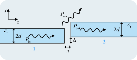
The geometry under consideration is shown in Fig. 1. A single mode slab waveguide of half-width and permittivity is broken by an offset in the axis, , and a gap in the axis . An eigenmode is incident from the left (input waveguide) carrying power , most of which is transmitted to the output waveguide (), while the remainder is either scattered () or reflected back into the input waveguide. No variations of the geometry are assumed along the axis, and therefore all quantities given are per unit length.

II A waveguide perturbed by an offset
First, we examine the case of no gap, , and a small offset . For the calculation of the fields we take an approach of mode matching approximation, similar to that described by Marcuse Marcuse (1970, 1972). We begin by considering a transverse electric (TE) incident mode, for which the nonzero field components are , , and . The even guided mode incident from the left is given inside the dielectric slab by , where , is the transverse wavenumber in the dielectric, is the longitudinal wavenumber, is the transverse decay constant outside the slab, and the time dependence is of the form . The transverse electric field in each region may be represented as a sum of the guided modes and the continuous spectrum of the radiation modes, corresponding to the scattered light. Explicitly, assuming the interface plane is at , then for (input waveguide) this field is given by
| (1) |
whereas for (output waveguide) it reads
| (2) |
In the above two equations, and are the reflection and transmission coefficients of the guided mode, respectively; and are the reflected and transmitted guided modes, respectively; and are the amplitudes of the even and odd radiation modes, respectively; is the transverse wavenumber of the radiation modes outside the slabs; and are the even and odd radiation modes, respectively. The amplitudes of the guided and the radiation modes may be approximated analytically by expressions containing the overlap integral between the respective mode and the incident guided mode.
Generally, force densities on dielectrics may be viewed as resulting from two processes Mizrahi and Schächter (2005); Schwinger et al. (1998); Mansuripur (2004): (1) the interaction of effective polarization volume current densities with the magnetic field, and (2) the interaction of polarization surface charge densities with the electric field. In the TE case, no component of the electric field is perpendicular to the boundaries of the dielectrics, and therefore no polarization surface charge densities are formed. Thus the time-averaged volume force density in the direction is given by , where is the polarization density. By integration over the volume, we obtain the total transverse force on the output waveguide in terms of integration over only the top and bottom surfaces
| (3) |
When there is no offset (), the field is symmetric around and the guided mode is not disturbed by a discontinuity, and thus no force acts on each of the waveguide parts. Once an offset is introduced, symmetry is broken, and scattering occurs from the discontinuity. The question then arises whether the two parts of the waveguide will tend to deflect away from each other, or self-align to form back a continuous waveguide while maximizing the output power.
For the evaluation of the force on the output waveguide, the field expression of Eq. (2) is substituted into Eq. (3). At this point, we are interested in small offsets, so that only terms up to the first order of are kept. Noting that cross-products of the even radiation modes with the odd radiation modes are of order larger than , and using the symmetry properties of the modes, the expression for the force reads
| (4) |
where the integration is performed at . Hence, it is evident that the odd radiation modes created by the scattering are responsible for the transverse force on the waveguide. A direct measure of the waveguide’s tendency to move either way is the derivative of the force with respect to , denoted by . Bearing in mind that , the force may be approximated by . The only term in the above equation that depends on is , and an analytic expression for may be obtained. The integration over is then performed analytically, and the closed form expression for the derivative reads
| (5) |
where . While the spectrum of radiation modes contains both propagating modes having real and evanescent modes having imaginary , the above expression shows that it is only the evanescent radiation modes that contribute to the generation of this force, i.e., the integrand is nonzero only for .
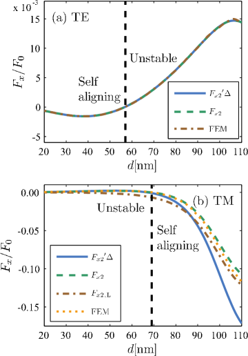
Both the force [Eq. (4)] and the quantity [Eq. (5)] are plotted in Fig. 2(a) as a function of , for an offset of 2% of . The range of shown is 20 nm to 110 nm, where the slab is single mode in each polarization. The wavelength is taken to be m and the permittivity is , corresponding to silicon at that wavelength. The forces are normalized by , which is the momentum per unit time carried by a plane wave. These results are compared with a Finite Element Method (FEM) simulation, and as seen the three curves are virtually identical. In addition to the integration of the force on the polarization densities, we have also integrated over the Maxwell stress tensor Schwinger et al. (1998) to obtain the force, and found excellent agreement between the two methods, which are mathematically equivalent for exact solutions of Maxwell’s equations.

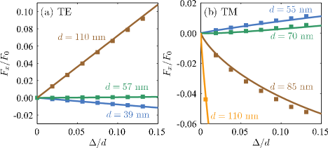
The plot of Fig. 2(a) reveals two regimes; the first is a self-alignment regime up to a slab half-width of about 57 nm, for which corresponding to a restoring force. The second is an instability regime in which a small offset results in a deflection force. Both regimes exhibit an optimal slab width for which the force is strongest. Although we show here only the transverse force on the output waveguide, when the offset is small, the scattered power is negligible and by virtue of momentum conservation, the force on the input waveguide is of the same magnitude and opposite in sign to that on the output waveguide. In fact, we have shown analytically that =-. To better illustrate the different regimes, we depict in Fig. 3(a) the transverse force as function of for nm where a negative restoring force is seen, nm where the force derivative at vanishes at the transition between the two regimes, and for nm where instability in the form of a deflecting force is observed.

When the incident mode is transverse magnetic (TM), the situation is considerably more involved. The field components for the TM mode are , , and , and the incident magnetic field is given by , where
The fields in each region are described by Eqs. (1) and (2) with replaced by . The force mechanism in the TM case differs substantially than that of the TE case, as for the TM the electric field has normal components to discontinuities in the dielectric, and therefore polarization surface charge densities are formed. These surface charge densities interact with to give rise to surface force densities. Considering again the output waveguide, the first contribution is from the polarization surface charge densities created by at the interface. The force density of this term is given by , where is the field just inside the slab at . Calculation of this force on the output waveguide while keeping only terms up to the first order of yields
| (6) |
where an analytic expression for may be obtained. A second contribution is from the polarization surface charge densities formed on the top () and bottom () parts of the waveguide, given by the plus and minus of , respectively. In both cases is the field just inside the slab. Summing up the two contributions and integrating over results in the expression
| (7) |
The third contribution comes from the volume force density given by , and integration over and gives
| (8) |
The total force is the sum of all three contributions, and its derivative is obtained by analytically differentiating . Similarly to the TE mode, only the evanescent part of the odd radiation mode spectrum participates in the generation of the force, and the relation holds as well.
The quantities , , as well as the force calculated by FEM, are shown in Fig. 2(b) as a function of for an offset of 2%. Contrary to the TE case, here instability occurs for small values of , and above about 70 nm there is self-alignment. The restoring force increases monotonically, so that at the maximum value in the shown range of , it is about two orders of magnitude stronger than the peak value of the TE restoring force. This dramatic difference is due to the presence of electric field components that are perpendicular to the dielectric boundaries. Specifically, at the left boundary of the output waveguide ( plane), induces a polarization surface charge density, while gives it a transverse kick. The result, given by Eq. (6), is plotted in Fig. 2(b). This force is negative for the entire range of and is seen to comprise almost all of the total force in the self alignment regime. Qualitatively, it may be associated with a dipole induced by the guided mode which has , and the strength of the dipole per power increases with as the mode confinement increases. At the interface, the dipole is roughly inverted, and consequently the two parts attract each other, in both the transverse and longitudinal directions. Moreover, this force grows rapidly as a function of and is therefore responsible for the derivative approximation being less accurate than for the TE case. This is seen in Fig. 3(b) where is plotted for four different values of : nm where instability is observed, nm about where the derivative vanishes at , nm which exhibits self alignment, and nm, where there is strong self alignment which is further discussed below.
III A waveguide broken by an offset and a gap
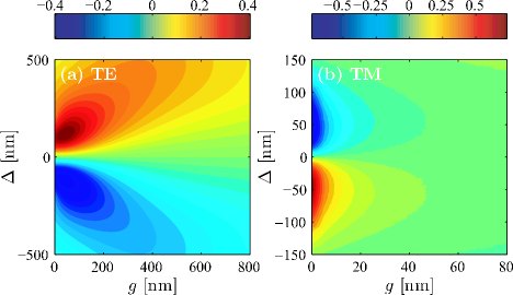
So far we have established the fundamental tendency of a waveguide to self-align or be in instability by considering zero gap and a perturbation in a continuous waveguide in the form of an offset. We next extend the discussion by introducing a longitudinal gap . Figure 4(a) and Fig. 4(b) show contours of in the – plane obtained by FEM simulations, for TE and TM incident modes, respectively. The slab half-width is assumed to be nm, where according to Fig. 2, the TE mode places the system in instability, whereas the TM mode causes self alignment. In both cases the behavior extends to larger values of , but the decay of the TE repulsive force with the offset and gap is much slower than that of the attractive TM force, as seen by the scales of and of the two frames of Fig. 2. The maximal TE force is about and it is obtained for about nm and nm. A waveguide cantilever at is, in fact, in a bistable state where a small offset may result in a deflection force that would eventually be balanced by the mechanical force. The attractive TM force is obtained for and nm, and it is about . We further found that a strong longitudinal force is pulling the two waveguides towards each other at a force of about for nm. For large enough values of the TM force becomes repulsive, corresponding to radiation pressure.
The self alignment and the instability may be tested experimentally by fabricating on a chip two waveguide cantilevers with an offset and a gap. For instance, for mW, pN, and at nm we obtain according to Fig. 2(b), which is about 10pN. This is of the order of magnitude of force that was shown to actuate a silicon cantilever Li et al. (2008). The deflection of the waveguide in such a system may be viewed by the nonlinear input/output behavior, as the output power increases when the cantilevers tend to self align. Moreover, the mechanical effect is doubled by the fact that a similar force opposite in sign is exerted on both cantilevers. The two cantilevers may also be vibrated at their mechanical resonance by modulating the incident power, resulting in a system that may be suitable for applications such as sensing.

IV Conclusion
In conclusion, we demonstrated a novel effect of light forces in the form of self alignment or instability of a waveguide broken by an offset and a gap. The waveguide size and mode polarization determine which of the two regimes the waveguide is in. Closed form expressions for the transverse forces were given for the case of a small offset and no gap. The forces described here are unique as they are due to the presence of both the guided mode and the scattered light from the discontinuity. Strong self alignment for a TM mode is caused by near field interaction of the polarization surface charges created by the longitudinal electric field. We are currently looking into the possibilities of an experimental realization that will demonstrate the effects discussed here.
ACKNOWLEDGMENTS
This work was supported by the Defense Advanced Research Projects Agency, the National Science Foundation, the NSF CIAN ERC, the U.S. Air Force Office of Scientific Research, the U.S. Army Research Office, and the Technion Viterbi Fellowship.
References
- Ashkin (1970) A. Ashkin, Phys. Rev. Lett. 24, 156 (1970).
- Grier (2003) D. G. Grier, Nature 424, 810 (2003).
- Notomi et al. (2006) M. Notomi, H. Taniyama, S. Mitsugi, and E. Kuramochi, Phys. Rev. Lett. 97, 023903 (2006).
- Kippenberg and Vahala (2008) T. J. Kippenberg and K. J. Vahala, Science 321, 1172 (2008).
- Tomes and Carmon (2009) M. Tomes and T. Carmon, Phys. Rev. Lett. 102, 113601 (2009).
- Eichenfield et al. (2007) M. Eichenfield, C. P. Michael, R. Perahia, and O. Painter, Nat. Photonics 1, 416 (2007).
- She et al. (2008) W. She, J. Yu, and R. Feng, Phys. Rev. Lett. 101, 243601 (2008).
- Xu et al. (2004) Q. Xu, V. R. Almeida, R. R. Panepucci, and M. Lipson, Opt. Lett. 29, 1626 (2004).
- Levy et al. (2005) U. Levy, M. Abashin, K. Ikeda, A. Krishnamoorthy, J. Cunningham, and Y. Fainman, Phys. Rev. Lett. 98, 243901 (2005).
- Tan et al. (2008) D. T. H. Tan, K. Ikeda, R. E. Saperstein, B. Slutsky, and Y. Fainman, Opt. Lett. 33, 3013 (2008).
- Povinelli et al. (2004) M. L. Povinelli, M. Ibanescu, S. G. Johnson, and J. D. Joannopoulos, Appl. Phys. Lett. 85, 1466 (2004).
- Povinelli et al. (2005) M. L. Povinelli, M. Lončar, M. Ibanescu, E. J. Smythe, S. G. Johnson, F. Capasso, and J. D. Joannopoulos, Opt. Lett. 30, 3042 (2005).
- Mizrahi and Schächter (2005) A. Mizrahi and L. Schächter, Opt. Express 13, 9804 (2005).
- Mizrahi and Schächter (2006) A. Mizrahi and L. Schächter, Phys. Rev. E 74, 036504 (2006).
- Mizrahi and Schächter (2007) A. Mizrahi and L. Schächter, Opt. Lett. 32, 692 (2007).
- Mizrahi et al. (2008) A. Mizrahi, M. Horowitz, and L. Schächter, Phys. Rev. A 78, 023802 (2008).
- Rakich et al. (2007) P. T. Rakich, M. A. Popović, M. Soljačić, and E. P. Ippen, Nat. Photonics 1, 658 (2007).
- Li et al. (2008) M. Li, W. H. P. Pernice, C. Xiong, T. Baehr-Jones, M. Hochberg, and H. X. Tang, Nature 456, 480 (2008).
- Marcuse (1970) D. Marcuse, Bell Syst. Tech. J. 49, 273 (1970).
- Marcuse (1972) D. Marcuse, Light Transmission Optics (Van Nostrand, New York, 1972).
- Mansuripur (2004) M. Mansuripur, Opt. Express 12, 5375 (2004).
- Schwinger et al. (1998) J. Schwinger, L. L. DeRadd, K. A. Milton, and W.-Y. Tsai, Classical Electrodynamics (Perseus Books, Reading, MA, 1998).