On the origin of the electric carrier concentration in graphite
Abstract
We investigate the dependence of the electrical resistivity and magnetoresistance of single crystalline micrometer-sized graphite samples of a few tens of nanometers thick on the defect concentration produced by irradiation at low fluences. We show that the carrier density of graphite is extremely sensitive to the induced defects for concentrations as low as ppm and follows with the distance between defects in the graphene plane. These and Shubnikov-de Haas oscillations results indicate that at least a relevant part of the carrier densities measured in graphite is not intrinsic.
pacs:
73.90.+f,61.80.-x,81.05.UwThe electronic properties of ideal graphite are actually not well known simply because defect-free graphite samples do not exist. In the last fifty years scientists flooded the literature with reports on different kinds of electronic measurements on graphite samples, providing evidence for carrier (electron plus hole) densities per graphene layer at low temperatures cm-2, see e.g. Refs. McClure, 1964; Kelly, 1981; Grüneis et al., 2008. Taking into account that: (1) an exhaustive experience accumulated in gapless semiconductors - whose density of states should be similar to its counterpart in a semimetal - indicates so far that the measured is most probably due to impurities Tsidilkovski (1997), and (2) the expected sensitivity of in graphite on lattice defects and impurities or adatoms Kelly (1981); Stauber et al. (2007), a fundamental question remains unanswered, namely, how large is the intrinsic of ideal graphite? Why is so important? Let us recapitulate some fundamental band structure theoretical results for the graphite structure Kelly (1981). Two-dimensional (2D) calculations assuming a coupling between nearest in-plane neighbors C-atoms give a carrier density (per C-atom) (eV and is the temperature). Introducing a coupling (eV) between C-atoms of type in adjacent planes one obtains ( are numerical constants). In both cases . Neither in single layer graphene nor in graphite such dependences were ever reported nT , i.e. a large density background was always measured and assumed as “intrinsic” without taking care of any influence from lattice defects (including edge effects Kobayashi et al. (2006)) or impurities. To fit experimental data and obtain a finite Fermi energy , up to seven free parameters were introduced in the past, whereas in the simplest case Kelly (1981); Dillon et al. (1977).
Clearly, any evidence that speaks against an intrinsic origin of - even a part of - the measured in graphite samples would cast doubts on the relevance of related electronic band structure parameters obtained in the past and will help significantly to clarify observed transport phenomena. As in the case of gapless semiconductors Tsidilkovski (1997) this requires a formidable experimental task. For example, to prove that the measured cm-2 in Ref. García et al., 2008 is due to vacancies/interstitials requires a vacancy resolution better than 0.05 ppm. Although nowadays the concentration of impurities in graphite can be measured with ppm resolution there is no experimental method that allows us to determine with such a precision the number of vacancies or C-interstitials. In spite of that and because of this situation we would like to start the discussion on the origin of postulating that at least part of it cannot be intrinsic. The studies presented here provide answers to: (1) Can a single vacancy/interstitial provide one carrier into the conduction band even if they are several hundreds of nm apart (ppm concentration)? This is a relevant issue specially because we expect that the Fermi wavelength in graphite m González et al. (2007). (2) Can the resistivity of graphite change with such small defect concentrations? (3) How reliable are band structure parameters of graphite obtained from the field-induced quantum oscillations in the resistivity (or magnetization)? (4) Why there is an apparent maximum value for cm-2 in graphite samples?
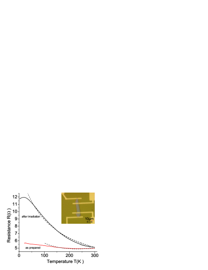
In this study we measured the change of the electrical resistance of thin crystalline graphite samples as a function of defect concentrations between to ppm. To do this we irradiated three nm thick and tens square micrometer samples under ambient conditions with a focused proton microbeam of 2.25 MeV energy scanned over the samples. A photo of sample 1 can be seen in Fig. 1. Particle induced x-ray emission measurements were done in situ and revealed a total concentration of g/g of non-magnetic impurities except hydrogen of concentration hho . The magnetoresistance of a fourth sample of size m3 was measured at three different parts, each of length m and irradiated with 30 keV Ga+ ions. In this sample Shubnikov-de Haas (SdH) oscillations were measured at 4K before and after irradiation and also for the corresponding bulk sample. Further details on the electron-beam spectroscopy and Raman techniques and the exfoliation and ultrasonic procedures use to characterize and prepare the crystalline thin graphite flakes from bulk samples will be published elsewhere.


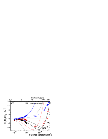
Figure 2(a) shows the relative change of the resistance vs. time during and after irradiation of sample 3 at 297 K. The curves are obtained at different initial relaxed states after application of a certain proton fluence. When the beam starts to hit the sample we observe a clear decrease in the resistance, whose amount depends on the fluence used and on the initial sample state. Figure 2(b) shows the resistance change relative to the sample virgin state. In this figure s means the time at which the beam stops irradiating the sample. Remarkable is that for all samples in the virgin state we observe a decrease in the resistance of a few percent for induced defect density ppm (average defect distance nm!) that remains after several hours after irradiation, i.e. in the relaxed state h), see curves (1-3) in Fig. 2(b). In Fig. 3 we show this relative change for samples 2 and 3. A further increase of the fluence increases the resistance in the relaxed state, see Fig. 3. The explanation for this behavior is that defects increase the carrier density , as theoretically suggested Stauber et al. (2007). Because defects also act as scattering centers, both the carrier mean free path and have to be taken into account.
We assume graphite as a structure composed of weakly-coupled graphene sheets Kopelevich and Esquinazi (2007). Within a factor of two the initial value at 297 K before irradiation for the carrier density is cm-2 and for the mean free path nm García et al. (2008). The smallness of at 297 K in comparison to the sample size allows us to use the Boltzmann-Drude semiclassical approach. This is important because for our sample sizes and at K there is no straightforward theoretical approach that includes ballistic and diffusive scattering that allows us to obtain in a simple way from the resistance. Hall effect measurements are not necessarily preferred to obtain since: - the Hall signal depends on at least six unknown parameters ( for electrons and holes independently) that change with defect concentration and ; - conventional multiband approaches appear to be inadequate for graphite García et al. (2008); - added to these difficulties, the Hall signal of graphite can be anomalous at K Kopelevich et al. (2006).
Following SRIM simulations Ziegler (1977-1985) the produced defect concentration at a proton fluence of cm-2 would be cm-2. Assuming that each defect in the graphene plane increases by one the carrier number, the increase in carrier density after irradiating such fluence will be , or in terms of the related wave vector cm. This simple estimate reveals that such small defect concentrations are relevant for the transport.


At 297 K the produced defects by irradiation are metastable met , see Fig. 2. Therefore, we plot in Fig. 3 the relative change of the resistance just at the end of the irradiation with respect to the virgin state , i.e. (close and open circles in Fig. 3). Another possibility is to plot the relative change with respect to the resistance taken one hour after irradiation , i.e. (close and open squares in Fig. 3). Both ways minimize the influence of annealing effects and provide a similar behavior. These relative changes indicate that the resistance reaches a minimum of its initial value at nm, see Fig. 3. At higher fluences the resistance increases because the decrease of starts to overwhelm the increase in .
A quantitative description of these data can be done taking into account the two dimensional resistivity Nomura and MacDonald (2006) , where are the Fermi velocity, the Fermi energy and the scattering relaxation time at Fermi energy. Using for clean graphene Stauber et al. (2007), the expression for and , one arrives at the simple expression . Furthermore, the carrier density increases as , where for one carrier per defect. Following Mathiessen’s rule, the mean free path is given by , where is the initial value due to all scattering centers before irradiation and the mean free path due to the produced defects. The relative change of resistance can be written as
| (1) |
The solid curve shown in Fig. 3 is obtained with cmcm for nm and . Within logarithmic corrections, the obtained function agrees quantitatively with that found in Ref. Stauber et al., 2007. In Fig. 3 we show also other curves obtained using other values for and pre-factors for as well as assuming the usual 3D relationship instead of . The comparison indicates that within a factor of two is indeed given by (for nm) and that the usual 3D relationship for cannot describe the observed behavior within a reasonable range of parameters.
The remarkable increase in K) and the observed change in the temperature dependence of graphite after inducing only ppm defect density (nm) is mainly given by the decrease of with temperature. As shown in Ref. García et al., 2008 is basically determined by thermal electrons (note that K for cm-2) and its dependence overwhelms that of . With , García et al. (2008) and the parameters obtained from Fig. 3 in Eq. (1) one can understand the observed temperature dependence of the resistance above K, see Fig. 1; at lower temperature the Boltzmann-Drude approach looses its validity.
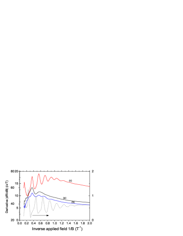
The band parameters of graphite were obtained mostly on macroscopic samples and usually from magneto-optical studies, SdH and de Haas-van Alphen oscillations, cyclotron resonance, etc. We doubt that in graphite samples the defect density is negligible and therefore we expect that the carrier density is neither small nor homogeneously distributed. Within the m length of sample 4 we measured the magnetoresistance at 4 K and calculate its first derivative in different parts of similar area. The SdH oscillations depend on the sample position, see Fig. 4, indicating clearly inhomogeneities in the carrier concentration within micrometers in agreement with EFM results that revealed sub-micrometer domainlike carrier density distributions in graphite surfaces Lu et al. (2006).
For the measured sample area that gives curve (a) in Fig. 4 and within experimental resolution there are no SdH oscillations up to a field T in clear contrast to the bulk sample, see Fig. 4. This fact can be understood assuming that in most of this sample part cm2. Then, the corresponding Fermi wavelength m is of the order of the sample size and larger than the cyclotron radius for T assuming ( is the free electron mass). In this case we do not expect to observe any SdH oscillations. However, for and 2.8 T two maxima are observed. From the measured “period” in as well as from the first field at which the first maximum appears we estimate the existence of domains of size nm in which nm, i.e. domains with cm-2 within a matrix of much lower carrier concentration. This indicates that the description of the SdH oscillations in real graphite samples can be achieved only within the framework of inhomogeneous 2D systems Dolgopolov et al. (1996); Harrison and Singleton (2001), an issue rarely studied in the past.
The selected Ga+ irradiation produced an average defect concentration of cm-2, i.e. ppm (Ga implantation ppm) in the thin graphite sample, “homogenizing” its carrier density distribution. After irradiation the SdH oscillations are clearly observed for T, see Fig. 4. Their period TT-1 is within the range found in literature Kelly (1981); Luk’yanchuk and Kopelevich (2004) and indicates cm-2.
Finally, if a relevant part of the reported carrier concentration in graphite is due to defects, why does it appear to saturate at cm-2 ( carrier per C-atom) ? We note that such saturation is also observed in gapless semiconductors with increasing donor concentration Tsidilkovski (1997). We might therefore expect it when the average distance between defects is of the order of the range of modification of the electronic structure produced by, e.g. a single vacancy, found experimentally to be nm Ruffieux et al. (2000) implying cm-2.
Concluding, the obtained results indicate that a concentration of defects (or impurities) of ppm can generate a carrier density cm-2 affecting the transport properties. This is an extraordinary sensitivity taking into account the large distances between defects these concentrations imply. Taking into account that, in best case, we have an impurity concentration ppm, except for hydrogen , plus an unknown concentration of vacancies and interstitials, we should doubt about the assumed “intrinsic” origin of the measured carrier concentrations in graphite. The behavior of SdH oscillations in micrometer-sized graphite regions and their changes after introducing defects support the above statement and indicate that real graphite is composed by an inhomogeneous distribution of carrier density.
Acknowledgements.
This work has been possible with the support of the DFG under DFG ES 86/16-1. S.D. is supported by BuildMona. One of the authors (P.E.) gratefully acknowledge correspondence with A. V. Krasheninnikov and F. Guinea.References
- McClure (1964) J. W. McClure, IBM J. Res. Dev. 8, 255 (1964).
- Kelly (1981) B. T. Kelly, Physics of Graphite (London: Applied Science Publishers, 1981).
- Grüneis et al. (2008) A. Grüneis, C. Attaccalite, T. Pichler, V. Zabolotnyy, H. Shiozawa, S. L. Molodtsov, D. Inosov, A. Koitzsch, M. Knupfer, J. Schiessling, et al., Phys. Rev. Lett. 100, 037601 (2008).
- Tsidilkovski (1997) I. M. Tsidilkovski, Electron Spectrum of Gapless Semiconductors, vol. 116 of Springer Series in Solid-State Sciences (Springer Verlag, 1997).
- Stauber et al. (2007) T. Stauber, N. M. R. Peres, and F. Guinea, Phys. Rev. B 76, 205423 (2007).
- (6) Note, however, that the data obtained in Ref. García et al., 2008 indicate cm (within factor of two), or with in [K].
- Kobayashi et al. (2006) Y. Kobayashi, K.-I. Fukui, T. Enoki, and K. Kusakabe, Phys. Rev. B 73, 125415 (2006).
- Dillon et al. (1977) R. O. Dillon, I. L. Spain, and J. W. McClure, J. Phys. Chem. Solids 38, 635 (1977).
- García et al. (2008) N. García, P. Esquinazi, J. Barzola-Quiquia, B. Ming, and D. Spoddig, Phys. Rev. B 78, 035413 (2008).
- González et al. (2007) J. C. González, M. Muñoz, N. García, J. Barzola-Quiquia, D. Spoddig, K. Schindler, and P. Esquinazi, Phys. Rev. Lett. 99, 216601 (2007).
- (11) W. Anwand, G. Brauer, D. Grambole, A. Setzer and P. Esquinazi, unpublished.
- Kopelevich and Esquinazi (2007) Y. Kopelevich and P. Esquinazi, Adv. Mater. (Weinheim, Ger.) 19, 4559 (2007).
- Kopelevich et al. (2006) Y. Kopelevich, J. C. M. Pantoja, R. R. da Silva, F. Mrowka, and P. Esquinazi, Physics Letters A 355, 233 (2006).
- Ziegler (1977-1985) J. F. Ziegler, The stopping and range of ions in matter (Pergamon Press, New York, 1977-1985).
- (15) A quantitative description of the observed time dependence (Fig. 2) shows that this is governed by interstitial migration processes Niwase (1995) and single vacancy diffusion Lee et al. (2005) with activation energies eV and eV, respectively. The migration processes annihilate partially the produced defects and at fluences (for sample 3) cm-2 the relaxed resistance increases indicating that the graphite structure remains with a certain amount of defects decreasing the overall carrier mobility.
- Nomura and MacDonald (2006) K. Nomura and A. H. MacDonald, Phys. Rev. Lett. 96, 256602 (2006).
- Lu et al. (2006) Y. Lu, M. Muñoz, C. S. Steplecaru, C. Hao, M. Bai, N. García, K. Schindler, and P. Esquinazi, Phys. Rev. Lett. 97, 076805 (2006), see also the comment by S. Sadewasser and Th. Glatzel, Phys. Rev. lett. 98, 269701 (2007) and the reply by Lu et al., idem 98, 269702 (2007); R. Proksch, Appl. Phys. Lett. 89, 113121 (2006).
- Harrison and Singleton (2001) N. Harrison and J. Singleton, J. Phys.: Condens. Matter 13, L463 (2001).
- Dolgopolov et al. (1996) V. T. Dolgopolov, A. A. Shashkin, G. V. Kravchenko, I. M. Mukhametzhanov, M. Wendel, J. P. Kotthaus, L. W. Molenkamp, and C. T. Foxon, JETP Lett. 63, 63 (1996).
- Luk’yanchuk and Kopelevich (2004) I. A. Luk’yanchuk and Y. Kopelevich, Phys. Rev. Lett. 93, 166402 (2004).
- Ruffieux et al. (2000) R. Ruffieux, O. Gröning, P. Schwaller, L. Schlapbach, and P. Gröning, Phys. Rev. Lett. 84, 4910 (2000).
- Niwase (1995) K. Niwase, Phys. Rev. B 52, 15785 (1995).
- Lee et al. (2005) G.-D. Lee, C. Z. Wang, E. Yoon, N.-M. Hwang, D.-Y. Kim, and K. M. Ho, Phys. Rev. Lett. 95, 205501 (2005).