Planar superconductor/ferromagnet hybrids: Anisotropy of resistivity induced by magnetic templates
Abstract
We investigated experimentally the transport properties of a superconducting cross-shaped aluminium microbridge fabricated on top of ferromagnetic BaFe12O19 single crystal. It was demonstrated that a one-dimensional domain structure in the ferromagnetic substrate can induce the formation of superconducting channels above magnetic domains. This leads to a giant anisotropy of resistivity of the superconducting bridge, caused by the appearance of continuous paths of supercurrents flowing along domain walls.
pacs:
74.78.-w 74.78.Fk 74.25.DwHybrid superconductor-ferromagnet (S/F) structures have attracted considerable attention in connection with the possibility to control thermodynamic and transport properties of the S/F hybrids by manipulating the magnetic state of the ferromagnetic constituents (Buzdin-RMP-05 ; Lyuksyutov-AdvPhys-05 ; Velez-JMMM-08 ; Aladyshkin-SuST-09 and references therein). Provided an insulating layer prevents the diffusion of Cooper-pairs from the superconductor to the ferromagnet, the exchange interaction between superconducting and ferromagnetic parts can be effectively suppressed and the interaction between both subsystems occurs via slowly decaying stray magnetic fields. Nonuniform magnetic field, induced by the ferromagnet, can modify the conditions for the appearance of superconductivity due to the effect of a local field compensation, resulting in the field-induced superconductivity Lange-PRL-03 and an exotic dependence of the superconducting critical temperature on an applied magnetic field Aladyshkin-PRB-03 ; Yang-Nature-04 ; Gillijns-PRB-07 . An increase of the width of the equilibrium magnetization loop of the S/F hybrids, compared with plain superconducting films, can be interpreted as an enhanced “magnetic” pinning of vortices by various magnetic textures: periodic arrays of magnetic dots Morgan-PRL-98 ; vanBael-PRB-99 or irregular magnetic bubble domains Lange-APL-02 . The magnetostatic interaction between the vortices and the “built-in” magnetic field is also known to lead to the unusual field dependence of the electrical resistance of the S/F hybrids at temperatures close to the superconducting critical temperature Lange-PRL-03 ; Martin-PRL-97 ; Jaccard-PRB-98 ; Hoffmann-PRB-00 .
Recently, electrical transport in S/F hybrids at low temperatures was studied for the following planar structures: Nb/Co Vodolazov-PRB-05 , Al/CoPd Morelle-APL-06 , NbSe2/Py Vlasko-Vlasov-PRB-08a , MoGe/Py Belkin-APL-08 ; Belkin-PRB-08 , Pb/Py Vlasko-Vlasov-PRB-08b . Superposition of the bias current and the supercurrent that is induced by hard ferromagnets may lead to a remarkable change of the current () – voltage () characteristics of superconducting bridges Vodolazov-PRB-05 ; Morelle-APL-06 , what can be interpreted as a “current” compensation effect Milosevic-PRL-05 . The tunable alignment of magnetic domains in low-coercive ferromagnetic films, using an in-plane oriented external field , makes it possible to introduce a guided vortex motion in a desirable direction – along the domain walls Vlasko-Vlasov-PRB-08a ; Belkin-APL-08 ; Belkin-PRB-08 ; Vlasko-Vlasov-PRB-08b .
In this Letter we are aiming at the investigation of the anisotropy of the electrical transport properties of the S/F hybrids, induced by a single straight domain wall. We measured both the magnetoresistance and the dependencies of a superconducting bridge in two perpendicular directions (i.e. along and across a domain wall in the ferromagnetic substrate).
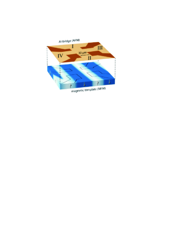
In order to study the anisotropy of the low-frequency transport properties in a planar S/F hybrid, we prepared a bi-layered sample consisting of a bulk ferromagnetic substrate and a thin-film Al microbridge on top. The ferromagnetic and superconducting parts were electrically isolated by a 5 nm SiO2 buffer layer, so that the interaction between these parts can be expected to be exclusively electromagnetic. When cut along the proper crystallographic direction, a ferromagnetic BaFe12O19 single crystal exhibits a one-dimensional (1D) stripe-type domain structure with dominant in-plane magnetization and relatively small out-of-plane component (the bottom image in Fig. 1). Measurements with a vibrating sample magnetometer (VSM) revealed that at low temperatures the magnetization of the used crystal depends almost linearly on the applied perpendicular magnetic field with the slope (A/m)T-1 and that it saturates at T. This means that external magnetic fields mT can only be of minor influence on the domain structure, since the variations of magnetic moment of the substrate are expected to be about 4.5% from the saturated magnetization (105 A/m). The location of the domain walls and their shape were determined by magnetic force microscopy (MFM), prior to the preparation of the Al bridge. The expected amplitude of the component of the nonuniform magnetic field, , exceeds the upper critical field of such Al films even at low temperatures (see below). The cross-shaped Al microbridge (50 nm thick) was fabricated by means of e-beam lithography, molecular beam epitaxy and lift-off etching (the top image in Fig. 1). The width of the ”arms” of the microbridge was equal to 30 m and limited by the width of the magnetic domains. Four contact pads, labelled in Fig. 1 as I–IV, were used for the injection of the dc bias current and for the measurement of the voltage drop for two different cases: along the domain wall () using the electrodes I and II and across the domain walls () using the electrodes III and IV. This symmetrical form of the superconducting element was intentionally chosen in order to have the possibility to compare the characteristics in two perpendicular directions for the same magnetic landscape.
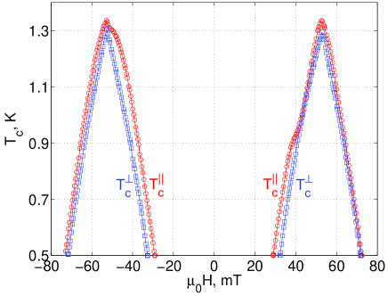
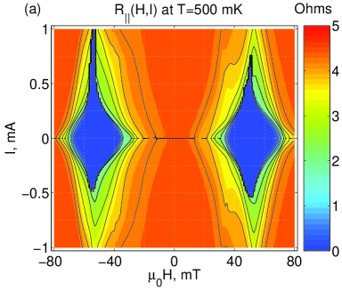
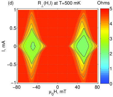
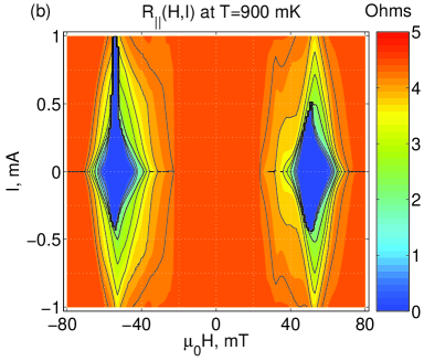
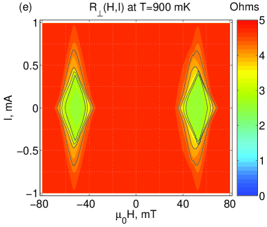
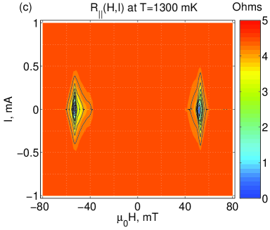
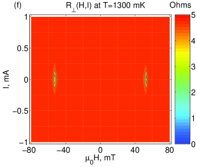
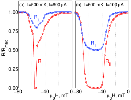
Figure 2 shows the level curves of the dc resistance of the sample, and , being the normal-state resistance, A. These lines can be commonly interpreted as the dependence of the superconducting critical temperature on . In spite of some inessential differences, both phase transition lines and have symmetrical maxima of similar amplitudes, and they are characterized by almost the same slope . In our opinion, this indicates that the nucleation of superconductivity, responsible for an initial deviation of the electrical resistance from its normal value, is almost isotropic (i.e. independent on the direction in which the bias current was injected and the voltage drop was recorded). Taking the position of the maxima and comparing the slope with that for the regime of surface superconductivity , we estimate the amplitude of the nonuniform field mT, the upper critical field mT at , and the maximal critical temperature K. These values appear to be typical for pure Al films and bridges Gillijns-PRB-07 .
However deeper in the superconducting state in the plane the transport properties of the S/F hybrid system become essentially anisotropic. Figure 3 illustrates this, showing the dependencies of the resistance (top row) and (bottom row) as a function of and , derived from the isothermal curves at constant value. As expected the total resistance of the sample goes to zero only for the parallel geometry when flows along domain walls [Fig. 3 (a)–(c)]. Indeed, the stripe-type domain structure allows to form a continuous path for the supercurrents at , connecting the electrodes I and II. It is easy to see that the maximal critical current corresponds to the most effective compensation, when one part of the bridge is subjected to zero local magnetic field, , while induces the normal state in the other part. Taking A and the sample’s cross-section cm2, one can estimate the critical current density A/cm2 at mK, which can be interpreted as the depinning current density. Apparently, an increase of temperature reduces the size of the area of zero resistance in the plane. By contrast, alternating superconducting and normal (N) regions, induced by the magnetic template, act as a series of resistors if is injected perpendicular to the S-N interfaces. Consequentially, the formation of superconductivity above the reverse domains roughly halves the total resistance of the sample at low temperatures: [Fig. 3 (d)–(f)]. Therefore, in the vicinity of the compensation fields, we observe a giant anisotropy of resistivity: (Fig. 4), which is in agreement with that obtained for a network of parallel magnetic domains in permalloy films Vlasko-Vlasov-PRB-08a ; Belkin-APL-08 ; Belkin-PRB-08 ; Vlasko-Vlasov-PRB-08b .
In summary, we demonstrated that a 1D domain structure in a ferromagnetic substrate can induce a giant anisotropy of the electrical transport of S films that are placed on top of the substrate. This effect is caused by the appearance of superconducting channels that run along the underlying magnetic domains. We also studied the - and dependence of the critical current through such an individual channel.
The authors are grateful to A.S. Mel’nikov, A.A. Fraerman and R. Kramer for stimulating discussions. This work was supported by the Methusalem Funding of the Flemish Goverment, NES – ESF program, the Belgian IAP, the Fund for Scientific Research – Flanders (F.W.O.–Vlaanderen), the Russian Fund for Basic Research, RAS under the program ”Quantum physics of condensed matter” and the Presidential grant MK-4880.2008.2.
References
- (1) A.I. Buzdin, Rev. Mod. Phys. 77, 935 (2005).
- (2) I.F. Lyuksyutov and V.L. Pokrovsky, Adv. Phys. 57, 67 (2005).
- (3) M. Vélez, J.I. Martín, J.E. Villegas, A. Hoffmann, E.M. González, J.L. Vicent, and I.K. Schuller, Journ. Magn. Magn. Mater. 320, 2547–2562 (2008).
- (4) A.Yu. Aladyshkin, A.V. Silhanek, W. Gillijns, and V.V. Moshchalkov, Supercond. Sci. Tech. 22, 053001 (2009).
- (5) M. Lange, M.J. van Bael, Y. Bruynseraede, and V.V. Moshchalkov, Phys. Rev. Lett. 90, 197006 (2003).
- (6) A.Yu. Aladyshkin, A.I. Buzdin, A.A. Fraerman, A.S. Melnikov, D.A. Ryzhov, A.V. Sokolov, Phys. Rev. B 68, 184508 (2003).
- (7) Z. Yang, M. Lange, A. Volodin, R. Szymczak, and V.V. Moshchalkov, Nature Mater. 3, 793 (2004).
- (8) W. Gillijns, A.Yu. Aladyshkin, A.V. Silhanek, and V.V. Moshchalkov, Phys. Rev. B 76, 060503(R) (2007).
- (9) D.J. Morgan and J.B. Ketterson, Phys. Rev. Lett. 80, 3614(1998).
- (10) M.J. Van Bael, K. Temst, V.V. Moshchalkov, and Y. Bruynseraede, Phys. Rev. B 59, 14674 (1999).
- (11) M. Lange, M.J. van Bael, V.V. Moshchalkov, and Y. Bruynseraede, Appl. Phys. Lett. 81, 322 (2002).
- (12) J.I. Martín, M. Vélez, J. Nogués, and I.K. Schuller, Phys. Rev. Lett. 79, 1929 (1997).
- (13) Y. Jaccard, J.I. Martín, M.-C. Cyrille, M. Vélez, J.L. Vicent, and I.K. Schuller, Phys. Rev. B 58, 8232 (1998).
- (14) A. Hoffmann, P. Prieto, and I.K. Schuller, Phys. Rev. B 61, 6958 (2000).
- (15) D.Y. Vodolazov, B.A. Gribkov, S.A. Gusev, A.Yu. Klimov, Yu.N. Nozdrin, V.V. Rogov, and S.N. Vdovichev, Phys. Rev. B 72, 064509 (2005).
- (16) M. Morelle and V.V. Moshchalkov, Appl. Phys. Lett. 88, 172507 (2006).
- (17) V. Vlasko-Vlasov, U. Welp, G. Karapetrov, V. Novosad, D. Rosenmann, M. Iavarone, A. Belkin, and W.-K. Kwok, Phys. Rev. B 77, 134518 (2008).
- (18) A. Belkin, V. Novosad, M. Iavarone, J. Fedor, J.E. Pearson, A. Petrean-Troncalli, and G. Karapetrov, Appl. Phys. Lett. 93, 072510 (2008).
- (19) A. Belkin, V. Novosad, M. Iavarone, J. Pearson, and G. Karapetrov, Phys. Rev. B 77, 180506 (2008).
- (20) V.K. Vlasko-Vlasov, U. Welp, A. Imre, D. Rosenmann, J. Pearson, and W.K. Kwok, Phys. Rev. B 78, 214511 (2008).
- (21) M.V. Milošević, G. Berdiyorov, and F.M. Peeters, Phys. Rev. Lett. 95, 147004 (2005).