Controllable spin-dependent transport in armchair graphene nanoribbon structures
Abstract
Using the non-equilibrium Green’s functions formalism in a tight binding model, the spin-dependent transport in armchair graphene nanoribbon (GNR) structures controlled by a ferromagnetic gate is investigated. Beyond the oscillatory behavior of conductance and spin polarization with respect to the barrier height, which can be tuned by the gate voltage, we especially analyze the effect of width-dependent band gap and the nature of contacts. The oscillation of spin polarization in the GNRs with a large band gap is strong in comparison with 2D-graphene structures. Very high spin polarization (close to ) is observed in normal-conductor/graphene/normal-conductor junctions. Moreover, we find that the difference of electronic structure between normal conductor and graphene generates confined states in the device which have a strong influence on the transport quantities. It suggests that the device should be carefully designed to obtain high controllability of spin current.
pacs:
75.75.+a, 72.25.-b, 05.60.Gg, 73.43.JnI introduction
Graphene, a monolayer of carbon atoms packed into a two dimensional (2D) honeycomb lattice, has attached a great amount of attention from both experimental and theoretical points of view cast09 since it was isolated and demonstrated to be stable novo04 ; novo05 . It is a basic building block for graphite materials of all other dimensionalities, e.g., it can be wrapped up into 0D fullerenes, rolled into 1D nanotubes, or stacked into 3D graphite. Due to its unique electronic properties, i.e., its conduction electrons behave as massless Dirac fermions novo05 ; zhan05 , a lot of interesting phenomena such as the finite conductance at zero concentration novo05 , the unusual half integer quantum Hall effect zhan05 , and the Klein tunneling stan09 have been observed in the graphene and theoretically discussed in the framework of the massless fermion Dirac’s model novo05 ; kats06 .
Finite width graphene strips, which are referred as graphene nanoribbons, have been also studied attentively naka96 ; cres08 ; koba06 ; han007 ; quer08 . It has been shown that GNRs of various widths can be obtained from graphene monolayers using patterning techniques han007 . The transport properties of the perfect GNRs are expected to depend strongly on whether they have zigzag or armchair edges naka96 . In the framework of the nearest neighbor tight binding (NNTB) model, the GNRs with zigzag edges are always metallic while the armchair structures are either semiconducting or metallic depending on their width. In the zigzag GNRs, the bands are partially flat around the Fermi energy [ eV], which means that the group velocity of conduction electrons is close to zero. Their transport properties are dominated by edge states koba06 . In the GNRs with armchair edges, the bands exhibit a finite energy gap in the semiconducting structures or are gapless in the metallic ones naka96 . However, ab initio studies have demonstrated that there are no truly metallic armchair GNRs (see in Ref. cres08 and reference therein). Even for the structures predicted to be metallic by the NNTB model, a small energy gap opens, thus modifying their behavior from metallic to semiconducting. In general, the group velocity of conduction electrons in armchair GNRs is high, e. g., it is constant and equal to about m/s novo05 in those metallic structures. The transport properties of ideal zigzag and armchair GNRs are thus very different. In the current work, we pay our attention only to the ribbons with armchair edges.
Experimentally, electronic transport measurements through a graphene sheet usually require contacts to metal electrodes, e.g., see an illustration in Ref. huar07 . When tunneling from metal reservoir to graphene occurs in a large area, the contact becomes Ohmic and the area under the contact forms a substance which is a hybrid between graphene and normal metal blan07 . Depending on the nature of this substance, the system can be appropriately considered as a graphene/graphene/graphene (GGG) structure or a normal-conductor/graphene/normal-conductor (NGN) junction whose contacts can be modeled by honeycomb or square lattices, respectively. The ballistic transport through the NGN systems has been investigated systematically in Refs. scho07 ; blan07 ; robi07 .
Beside their interesting electronic transport properties, due to very weak spin orbit interaction kane05 , which leads to a long spin flip length () jozs08 , the graphene - based structures also offer a good potential for spin-polarized electronics. Actually, graphene is not a natural ferromagnet. However, recent works have shown that ferromagnetism and spin-polarized states can be introduced in graphene, e. g., by doping and by defect pere05 ; wehl08 ; yazy07 or by applying an external electric field son006 . Especially, Haugen et. al. haug08 suggested that the ferromagnetic correlations can be created in graphene by the so-called proximity effect. The exchange splitting induced by depositing a ferromagnetic insulator on the graphene sheet was then roughly estimated to be about meV. The effect has been also experimentally demonstrated jozs08 ; hill06 . Motivated by these features, some other works have predicted and discussed the controllability of spin current by a ferromagnetic gate in -graphene structures yoko08 ; vndo08 ; zou009 . The spin current was found to be an oscillatory function of the potential barrier, which can be tuned by the gate voltage, and its amplitude is never damped by the increase of the width and the height of barrier yoko08 . However, the spin polarization is not so high, e. g., its maximum value is just about . In addition, the other spin-dependent properties of graphene such as spin field effect transistor seme07 , spin Hall effects kane05 ; sini06 , spin valve effects cho007 ; brey07 ; roja09 ; saff09 have been also investigated extensively. Especially, the giant magneto-resistance has been explored theoretically and discussed in the structures of armchair saff09 and zigzag roja09 GNRs connecting two conducting electrodes. The authors predicted that it can reach the high value of roja09 .
In this article, we are interested in the possibilities of electrically tunable of spin current in single ferromagnetic gate armchair GNR structures. By investigating the physics of spin polarized transport in these structures, we would like to derive some simple scaling rules in order to tend to a high tunable spin polarized current. The study is focussed on the role of the ribbon’s energy band gap and the different types of leads (either graphitic or normal-conducting). In the NGN systems, since the strength of the device-to-contact coupling and the device length are important parameters, their influence on the control of spin current is also carefully investigated. The paper is organized as follows. Section 2 is devoted to the description of the model and main formulas based on the non-equilibrium Green’s functions formalism (NEGF). In section 3, the numerical results are presented and discussed. Finally, a brief summary is given in section 4.
II model and formulation
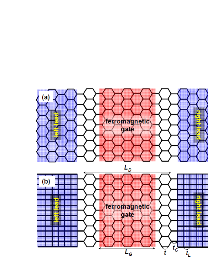
The considered structures consist of an armchair GNR coupled with two electrodes which may be described either by graphitic (Fig. 1(a)) or normal-conducting (Fig. 1(b)) leads. In the simplest consideration, the normal-conducting leads are modeled by square lattices blan07 ; scho07 ; robi07 . A ferromagnetic gate is assumed to create a potential barrier which controls the Fermi level locally and to induce an exchange splitting into the device. To model the structures, we use the single band tight binding Hamiltonian
| (1) |
where are the Hamiltonian of the left and right leads, respectively; is the Hamiltonian of the device; describes the coupling of the device to the leads. The Hamiltonian terms in Eq. (1) can be written as
| (2) | |||||
where the operators () and () create (annihilate) an electron with spin in the electrode and the device region, respectively. The sum over carbon atoms is restricted to the nearest neighbor atoms. , and stand for the hopping parameters in the device, the lead and at the coupling interface, respectively. is the on-site energy of the leads which acts as a shift in energy. The device spin-dependent on-site energy is modulated by the gate voltage
| (3) |
Here, denotes the potential barrier height, is the exchange splitting and describes the up/down spin states.
Since no spin flip process is considered here, (1) can be decoupled into two linear spin-dependent Hamiltonians and the transport is easily considered using the NEGF formalism. For each spin channel , the retarded Green’s function is defined as
| (4) |
where, describes the retarded self energy matrices which contain the information on the electronic structure of the leads and their coupling to the device. It can be expressed as where is the hopping matrix that couples the device to the leads. are the surface Green’s functions of the uncoupled leads, i.e., the left or right semi-infinite electrodes. The surface Green’s functions and the device Green’s functions are calculated using the fast iterative scheme sanc84 and the recursive algorithm anan08 , respectively.
Within the model described by Eq. (1), the transport is considered to be ballistic and the conductance through the device is calculated using the Landauer formalism imry99 . The spin-dependent conductances at the Fermi energy are obtained from the transmission function , such that
| (5) |
and
| (6) |
Here, () denotes the advanced Green’s function. The tunneling rate matrix for the left (right) lead is obtained from
| (7) |
where () is the advanced self energy. Finally, the spin polarization is determined by
| (8) |
In addition, the local density of states (LDOS) at site can be also directly extracted from the retarded Green’s function as:
| (9) |
By using the recursive algorithm described in Ref. anan08 , the size of matrices equals the number of carbon chains between two edges. Thus, the cost of calculations is only linearly dependent on the device length.
III results and discussion
Using the above formalism, we investigate the spin-dependent transport in the considered structures. Throughout the work, we set eV chic96 in the graphitic regions and assume that is equal to and in the NGN junctions blan07 ; robi07 . Our consideration is restricted to the low-energy regime when .
III.1 Gate control of spin current in GGG structures
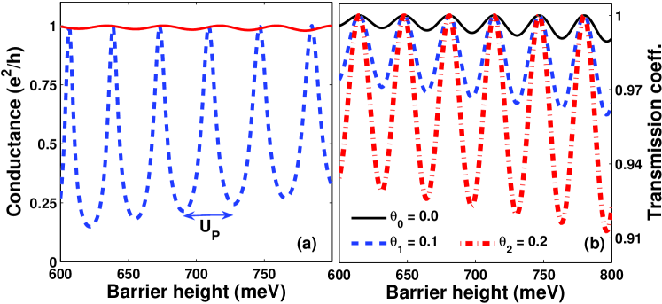
As mentioned above, the gate voltage creates a potential barrier in the device. In the armchair GNRs, the electronic properties of the structures with and ( is an integer) are significantly different, i. e., there is a finite energy band gap in the former structures while it is negligible in the latter ones cres08 . Respectively, we display in Fig. 2(a) the conductance as a function of the barrier height for the structures: (dashed) and (solid line). Here, the gated region is assumed to be nonmagnetic, i. e., meV. First of all, the results show that the conductance has an oscillatory behavior with respect to . This phenomenon has been observed in the -graphene structures and explained as a consequence of the well-known Klein’s tunneling kats06 ; yoko08 . In the framework of the Dirac’s description, the conductance peaks have been demonstrated to be essentially due to the resonance or the good matching of electron states and confined hole states outside/inside the barrier region vndo08 , respectively. Those states, in this model, correspond to electron states in positive and negative energy bands. Note that due to the finite ribbon width, the transverse momentum is quantized into a set of discrete values. Practically, the oscillation of conductance can be seen clearly from the analytical expression of the transmission coefficient for a given transverse momentum mode (see the calculation in Ref. klym08 ). In the limit of low energy, it can be rewritten as
| (10) |
where and with and is the bond length. () denotes the longitudinal (transverse) momentum, which is the deviation of the momentum from the zero energy point, outside the barrier and is the longitudinal momentum inside the barrier. The energy dispersions outside/inside the barrier are, respectively
| (11) | |||||
| (12) |
Accordingly, the transmission and then the conductance have their maximum (or minimum) values when is equal to (or ) for any integer . In the limit of , the eq. (12) can be rewritten as and the period of oscillation is defined by , which coincides with that in Refs. yoko08 ; vndo08 . In general cases, when the relation between and is nonlinear, the period can be approximately expressed as with . For instance, and for and presented in Fig. 2(a), respectively.
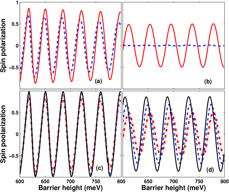
As a consequence of different electronic structures, the Fig. 2(a) also shows that the conductance for the case of (large energy gap) oscillates strongly in comparison with the other (). This can be easily understood by considering the behavior of transmission coefficient for different energy gaps. As seen in Eq. (11), the energy gap is enlarged when increasing (or ). So that, from the Eq. (10) and the Fig. 2(b), we see that when the energy gap is larger (increasing ), the oscillation of transmission is stronger. It leads to the different behaviors of conductance shown in Fig. 2(a). Similarly, it is shown that the oscillation of conductance in the structure with is also stronger than that in the -graphene structures (see in Fig. 2(a) of Ref. yoko08 ), where the gap is truly zero.
In eqs. (10-11), the mode (or ) corresponds essentially to the normal incident mode whose energy dispersion is gapless and linear in the -graphene structures. When considering the behavior of transmission coefficient, we find an important feature: it is not uniformly equal to unity, but a function of the barrier height even in the case of . This differs from the prediction of Klein’s paradox obtained by using Dirac’s description in graphene structures kats06 as previously discussed in Ref. tang08 . Practically, the transmission coefficient (eq. (10)) approaches the simplified expression (4) in Ref. kats06 only in the limit of .
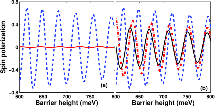
Now we investigate the behavior of spin polarization in the ferromagnetic gate structures. The exchange splitting is chosen to be meV, which can be achieved experimentally jozs08 ; hill06 . Since no spin flip process is considered, the exchange splitting just shifts the conductance of each spin channel relatively to the other. The spin polarization therefore behaves as an oscillatory function of as shown in Fig. 3. Similar phenomena in the -graphene structures have been also observed and discussed in Ref. yoko08 ; vndo08 ; zou009 . It was shown that the oscillation of spin current is never damped with the increase of the width and the height of barrier and the spin polarization can be reversed by changing the gate voltage. Actually, the amplitude of depends primarily on the phase coherence/decoherence of the oscillation of spin - dependent conductances, i. e., it has the maximum/minimum value when the gate length (or the barrier width) is equal to a half-integer/integer of with , respectively. Hence, the gate control of spin current can be modulated by changing , i. e., it leads to the beating behavior of similar to that shown in Fig. 5(c) of Ref. vndo08 . Furthermore, as a consequence of the behavior of conductance presented in Fig. 2(a), Fig. 3(a) also shows that the oscillation of in the GNRs with a large energy gap is very strong in comparison with the others. For instance, the amplitude of is about for while it is only few percents for or has a maximum value of in the -graphene structures yoko08 ; vndo08 ; zou009 . However, since for the energy gap decreases when increasing the ribbon width, the oscillation of conductance and in those structures is gradually weaker. The transport quantities for the GNRs in the limit of infinite width approaches those for the -graphene structures, where the continuum Dirac’s description is valid. To illustrate this point, we display in Fig. 3(b) an example of the effect of different ribbon widths on the spin polarization in the structures with . Indeed, when increasing the ribbon width, the amplitude of decreases and becomes closer to that in 2D-graphene, i. e., it is only about for .
III.2 Effects of normal-conducting leads
In this section, we consider the spin transport in NGN junctions. First, we focus on the possibilities of obtaining high tunable spin current when replacing the graphitic leads by the normal-conducting ones. Second, we analyze the sensitivity of transport quantities to different parameters as the device length and the Fermi energy.
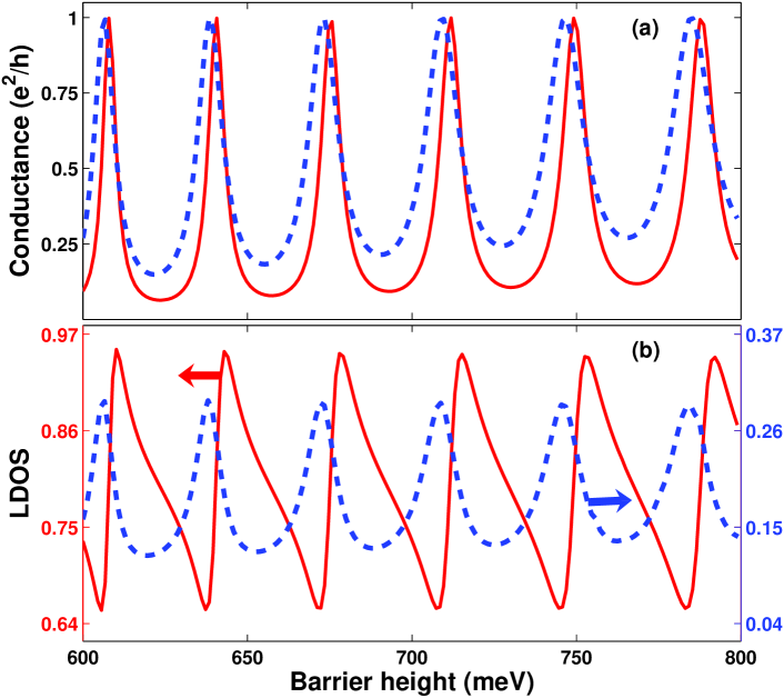
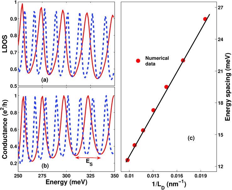
In Ref. scho07 , Schomerus compared the resistances of NGN junctions and GGG structures, and found the duality between graphitic and normal-conduncting contacts. He has shown that identical transport properties arise when the graphitic leads are replaced by quantum wires and the difference between the results obtained in those structures is only quantitative. On this basis, we plot in Fig. 4(a) the conductance as a function of in the NGN junction in comparison with the GGG structure for the case of nm and meV. Since we found that the results depend weakly on the hopping energy in the leads, is chosen to be equal to for simplicity. Qualitatively, Fig. 4(a) shows that the oscillation of conductance seem to be unchanged in its phase and period when changing the leads. Quantitatively, the oscillation in the NGN junction is stronger than in the GGG structure. This can be explained clearly by the effect of replacing the graphitic leads by the normal conducting ones on the picture of bound states in the barrier region. These states, in the framework of the Dirac’s description, have been considered as confined hole states in the -graphene structures vndo08 . In Fig. 4(b), we display the LDOS (see the right axis for graphitic and the left axis for normal-conducting leads) at the first site of barrier region with respect to . The results are understood that the peaks of LDOS occur when the Fermi energy corresponds to any bound state. Obviously, the oscillation of LDOS (or the quantization of bound states in the barrier) in the NGN junction appears stronger (with higher peaks) than that in the GGG structure. It is the essential origin of the different behaviors of conductance as shown in Fig. 4(a).
Now we turn to the behavior of spin current in ferromagnetic gate NGN junctions, i. e., meV. In Figs. 5(a) and 5(b), we display the comparison of spin polarization in the NGN junctions and the GGG structures. Due to the different behaviors of conductance shown in Fig. 4(a), the amplitude of in former structures is remarkably larger than that in latter ones. Particularly, when changing the leads, it increases from to (see in Fig. 5(a)) and from to (see in Fig. 5(b)) for and , respectively. Moreover, in the NGN junctions, the possibility of obtaining high tunable spin current is more impressive with decreasing the strength of the device-to-contact coupling, which is characterized by the hopping energy . In Figs. 5(c) and 5(d), we plot the obtained results for three cases: (dotted), (dashed) and (solid lines). Actually, the transport in these structures depends strongly on the properties of junctions and therefore on . A smaller corresponds to a higher contact resistance blan07 . We find that the quantization of bound states in the barrier region is stronger when decreasing (not shown), which leads to a stronger oscillation of the transport quantities with respect to the barrier height. Indeed, even in the case of , the spin polarization can reach a very high value of for (see in Fig. 5(d)). More impressively, in the cases of , it can tend to by reducing (see in Fig. 5(c)). A similar feature (giant magneto resistance) has been also predicted in the structures of GNRs connecting two conducting electrodes roja09 ; saff09 .
Practically, the features discussed above depend strongly on the parameters of the NGN junctions, such as the device length and/or the Fermi energy. It results from the fact that the charge transport can be confined in the device by two normal-conductor/graphene junctions. It leads to an additional resonant condition controlling the transport picture beside the transmission via the bound states in the barrier. Indeed, the existence of such confined states is demonstrated clearly from the behavior of LDOS shown in Fig. 6(a). In this figure, to cancel the effects of bound states in the barrier, the gate voltage is not applied to the device. The energy spacing is estimated to be about meV for nm and meV for nm. It means that seems to be inversely proportional to the device length, i. e., as illustrated in Fig. 6(c). This implies an unusual quantization of charges in the graphene-based structures, which is essentially different from the case of normal semicondutors wherein as previously discussed in Refs. vndo08 ; milt06 . Due to such confinement, the transport quantities, such as the conductance and the spin current (not shown), have an oscillatory behavior also with respect to the Fermi energy in the considered region (see in Fig. 6(b)). Therefore, when a gate voltage is applied, there is a coexistence of bound states in the barrier and confined states in the device. They together respond for the resonant transport conditions of the structure.
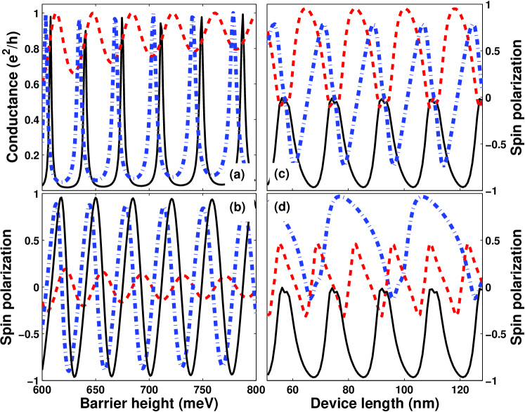
On the other hand, the gate controllability of spin current is principally due to the picture of bound states in the barrier (or Klein’s tunneling) vndo08 . It arises a question about how the confined states in the device affect that picture. As shown in Figs. 4 and 5, the replacement of the graphitic leads (infinite ) by normal-conducting ones (finite ) does not affect the period, but the amplitude of the oscillation. It suggests that, in the NGN junctions, the oscillation of conductance and spin polarization can be modulated in its amplitude while its period is unchanged when changing the device length. To examine this statement, we plot the conductance in Fig. 7(a) and the spin polarization in Fig. 7(b) as functions of the barrier height for different device lengths. From Fig. 7(a), we see that while the period is determined only by the gate length, the oscillation of conductance is modified by changing , i. e., it is strong/weak when (and ) or nm, respectively. Consequently, the amplitude of spin polarization is dependent on , i. e., it is about for nm, for nm and for nm (see Fig. 7(b)). This feature is exhibited more clearly in Fig. 7(c) by three curves of spin polarization versus for different barrier heights: (dashed), (dashed-dotted), and 681.5 (solid line) meV. We see that the spin current has an oscillatory behavior and is suppressed completely at certain values of . Obviously, this demonstrates that the amplitude of spin polarization exhibited in Fig. 7(b) is also an oscillatory function of the device length. Moreover, its period seems to be inversely proportional to the Fermi energy, i. e., it is about nm for meV, nm for meV and nm for meV (see Fig. 7(d)). It is nothing, but a consequence of the resonant transport due to the confined states in the device. Hence, the gate control of spin current in the NGN junction can be modulated not only by the gate length (see in the section A) but also by the device length and/or the Fermi energy . This implies that the structure should be carefully designed to obtain high controllability of spin current.
IV conclusions
Using the NEGF method for quantum transport simulation within a tight binding hamiltonian, we have considered the spin-dependent transport in single ferromagnetic gate armchair GNR structures. The leads are modeled as either graphitic or normal-conducting.
In the case of graphitic leads, it is shown that the conductance and the spin current behave as oscillatory functions of barrier height which can be tuned by the gate voltage. The oscillation of spin polarization in the ribbon structures with a large energy band gap is strong in comparison with the -graphene structures. Especially, the study has demonstrated that a very high spin polarization can be observed in the NGN junctions. It results from the fact that the quantization of bound states in the barrier (gated) region can appear very strong when using the normal-conducting leads. In this structure, it is shown that the spin polarization increases and can tend to with the decrease of the strength of the device-to-contact coupling. Moreover, we have also found the existence of confined states in the device by normal-conductor/graphene junctions. This confinement responds for an additional resonant condition beside the transmission via the bound states in the barrier. Therefore, the gate control of spin current in the NGN junctions can be modulated not only by the gate length but also by the device length and/or the Fermi energy.
Our predictions may be helpful for designing efficient spintronics devices based on perfect armchair GNRs. However, some disorder effects, e. g. due to edge roughness, have been observed experimentally han007 and demonstrated to affect the transport properties quer08 of the GNR structures. Further work is needed to assess their influence on the spin polarized properties discussed in this article.
Acknowledgements. This work was partially supported by the European Community through the Network of Excellence NANOSIL.
References
- (1) A. H. Castro Neto, F. Guinea, N. M. R. Peres, K. S. Novoselov and A. K. Geim, Rev. Mod. Phys. 81, 109 (2009)
- (2) K. S. Novoselov, A. K. Geim, S. V. Morozov, D. Jiang, Y. Zhang, S. V. Dubonos, I. V. Grigorieva and A. A. Firsov, Science 306, 666 (2004)
- (3) K. S. Novoselov, A. K. Geim, S. V. Morozov, D. Jiang, M. I. Katsnelson, I. V. Grigorieva, S. V. Dubonos and A. A. Firsov, Nature (London), 438, 197 (2005)
- (4) Y. Zhang, Y.-M. Tan, H. L. Stormer and P. Kim, Nature (London), 438, 201 (2005)
- (5) N. Stander, B. Huard and D. Goldhaber-Gordon, Phys. Rev. Lett. 102, 026807 (2009)
- (6) M. I. Katsnelson, K. S. Novoselov and A. K. Geim Nat. Phys. 2, 620 (2006)
- (7) M. Y. Han et al., Phys. Rev. Lett. 98, 206805 (2007); Z. Chen et al., Physica E 40, 228 (2007); X. Li et al., Science 319, 1229 (2008)
- (8) K. Nakada, M. Fujita, G. Dresselhaus and M. S. Dresselhaus, Phys. Rev. B 54, 17954 (1996)
- (9) Y. Kobayashi, K. Fukui, T. Enoki, K. Kusakabe, Phys. Rev. B 73, 125415 (2006)
- (10) A. Cresti, N. Nemec, B. Biel, G. Niebler, F. Triozon, G. Cuniberti and S. Roche, Nano Res. 1, 361 (2008)
- (11) D. Querlioz et al., Appl. Phys. Lett. 92, 042108 (2008); A. Lherbier et al., Phys. Rev. Lett. 100, 036803 (2008); M. Evaldsson et al., Phys. Rev. B 78, 161407(R) (2008)
- (12) B. Huard, J. A. Sulpizio, N. Stander, K. Todd, B. Yang and D. Goldhaber-Gordon, Phys. Rev. Lett. 98, 236803 (2007)
- (13) M. Ya. Blanter and I. Martin, Phys. Rev. B 76, 155433 (2007)
- (14) H. Schomerus, Phys. Rev. B 76, 045433 (2007)
- (15) J. P. Robinson and H. Schomerus, Phys. Rev. B 76, 115430 (2007)
- (16) C. L. Kane and E. J. Mele, Phys. Rev. Lett. 95, 226801 (2005)
- (17) C. Jzsa, M. Popinciuc, N. Tombros, H. T. Jonkman and B. J. van Wees, Phys. Rev. Lett. 100, 236603 (2008)
- (18) E. W. Hill, A. K. Geim, K. Novoselov, F. Schedin, and P. Blake, IEEE Trans. Magn. 42, 2694 (2006)
- (19) N. M. R. Peres, F. Guinea and A. H. Castro Neto, Phys. Rev. B 72, 174406 (2005)
- (20) T. O. Wehling, K. S. Novoselov, S. V. Morozov, E. E. Vdovin, M. I. Katsnelson, A. K. Geim and A. I. Lichtenstein, Nano Lett. 8, 173 (2008)
- (21) O. V. Yazyev and L. Helm, Phys. Rev. B 75, 125408 (2007)
- (22) Y.-W. Son, M. L. Cohen and S. G. Louie, Nature 444, 347 (2006)
- (23) H. Haugen, D. Huertas-Hernando and A. Brataas, Phys. Rev. B 77, 115406 (2008)
- (24) T. Yokoyama, Phys. Rev. B 77, 073413 (2008)
- (25) V. Nam Do, V. Hung Nguyen, P. Dollfus and A. Bournel, J. Appl. Phys. 104, 063708 (2008)
- (26) J. Zou, G. Jin and Y. -Q. Ma, J. Phys.: Condens. Matter 21, 126001 (2009)
- (27) Y. G. Semenov, K. W. Kim and J. M. Zavada, Appl. Phys. Lett. 91, 153105 (2007)
- (28) N. A. Sinitsyn, J. E. Hill, H. Min, J. Sinova and A. H. MacDonald, Phys. Rev. Lett. 97, 106804 (2006)
- (29) S. Cho, Y.-F. Chen, and M. S. Fuhrer, Appl. Phys. Lett. 91, 123105 (2007)
- (30) L. Brey and H. A. Fertig, Phys. Rev. B 76, 205435 (2007)
- (31) A. Saffarzadeh and M. Ghorbani Asl, Eur. Phys. J. B 67, 239 (2009)
- (32) F. Munoz-Rojas, J. Fernandez-Rossier, and J. J. Palacios, Phys. Rev. Lett. 102, 136810 (2009)
- (33) M. P. Lopez Sancho, J. M. Lopez Sancho and J. Rubio, J. Phys. F: Met. Phys. 14, 1205 (1984)
- (34) M. P. Anantram, M. S. Lundstrom and D. E. Nikonov, IEEE Proceeding 96, 1511 (2008)
- (35) Y. Imry and R. Landauer, Rev. Mod. Phys. 71, S306 (1999)
- (36) L. Chico, V. H. Crespi, L. X. Benedict, S. G. Louie and M. L. Cohen, Phys. Rev. Lett. 76, 971 (1996)
- (37) Y. Klymenko, L. Malysheva and A. Onipko, Phys. Stat. Sol. (b) 245, 2181 (2008)
- (38) C. Tang, Y. Zheng, G. Li and L. Li, Solid State Commun. 148, 455 (2008)
- (39) J. M. Pereira, Jr., V. Mlinar, F. M. Peeters and P. Vasilopoulos, Phys. Rev. B 74, 045424 (2006)