Screening in gated bilayer graphene
Abstract
The tight-binding model of a graphene bilayer is used to find the gap between the conduction and valence bands, as a function of both the gate voltage and as the doping by donors or acceptors. The total Hartree energy is minimized and the equation for the gap is obtained. This equation for the ratio of the gap to the chemical potential is determined only by the screening constant. Thus the gap is strictly proportional to the gate voltage or the carrier concentration in the absence of donors or acceptors. In the opposite case, where the donors or acceptors are present, the gap demonstrates the asymmetrical behavior on the electron and hole sides of the gate bias.
pacs:
73.20.At, 73.21.Ac, 73.43.-f, 81.05.UwBilayer graphene has attracted much interest partly due to the opening of a tunable gap in its electronic spectrum by an external electrostatic field. Such a phenomenon was predicted by McCann and Fal’ko McF and can be observed in optical studies controlled by applying a gate bias OBS ; ZBF ; KHM ; LHJ ; ECNM ; NC . In Refs. Mc ; MAF , within the self-consistent Hartree approximation, the gap was derived as a near-linear function of the carrier concentration injected in the bilayer by the gate bias. Recently, this problem was numerically considered GLS using the density functional theory (DFT) and including the external charge doping involved with impurities. The DFT calculation gives the gap which is roughly half of the gap obtained in the Hartree approximation. This disagreement was explained in Ref. GLS as a result of both the inter- and intralayer correlations.
In this Brief Report, we study this problem within the same Hartree approximation as in Refs. Mc ; MAF , but including the external doping. We consider the case, where the carrier concentration in the bilayer is less than 1013 cm-2, calculating the carrier concentration on both layers. Then, we minimize the total energy of the system and find self-consistently both the chemical potential and the gap induced by the gate bias. Our results completely differ from those obtained in Refs. Mc ; MAF even for the range where the external doping is negligible. The dependence of the gap on the carrier concentration, i. e., on the gate voltage, exhibits an asymmetry at the electron and hole sides of the gate bias.
The graphene bilayer lattice is shown in Fig. 1. Atoms in one layer, i. e., and in the unit cell, are connected by solid lines, and in the other layer, e. g., and , by the dashed lines. The atom () differs from () because it has a neighbor just below in the adjacent layer, whereas the atom () does not.
Let us recall the main results of the Slonchewski–Weiss–McClure model SW ; McCl . In the tight-binding model, the Bloch functions of the bilayer are written in the form
| (1) | |||
where the sums are taken over the lattice vectors and is the number of unit cells. Vectors and connect the nearest atoms in the layer and in the neighbor layers, correspondingly.

For the nearest neighbors, the effective Hamiltonian in the space of the functions (Screening in gated bilayer graphene) contains the hopping integrals and PP . The largest of them, , determines the band dispersion near the point in the Brillouin zone with a velocity parameter . The parameters and giving a correction to the dispersion are less than by a factor of 10 (see Refs. KHM ; LHJ ). The parameters and result in the displacements of the levels at , but is much less than . Besides, there is the parameter induced by the gate and describing the asymmetry of two layers in the external electrostatic field. This parameter simply presents the potential energy between two layers, , where is the interlayer distance and is the electric field induced both by the gate voltage and the external charge dopants in the bilayer. In the simplest case, the effective Hamiltonian can be written as
| (2) |
where the matrix elements are expanded in the momentum near the points.
The Hamiltonian gives four energy bands:
| (3) | |||
where
and we denote .
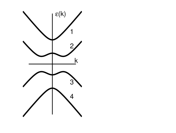
The band structure is shown in Fig. 2. The minimal value of the upper energy is . The band takes the maximal value at and the minimal value at Because the value of is much less than , the distinction between and is small and the gap between the bands and takes the value .

The eigenfunctions of the Hamiltonian (2) have the form
| (4) |
where the norm squared is
The probability to find an electron, for instance, on the first layer is , as seen from Eqs. (Screening in gated bilayer graphene).
We assume, that carriers occupy only the bands , so the chemical potential and the gap are less than the distance between the bands and , i. e., The electron dispersion for the bands can be expanded in powers of :
Then, for , we can use the simple relations:
| (5) | |||
Within such the approximation, many observable effects can be analytically evaluated for the intermediate carrier concentration, , where we neglect the effect of the ”mexican hat”.
At zero temperature, for the total carrier concentration and the carrier concentrations on the layers, we obtain
| (6) | |||
| (7) | |||
where cm-2 and .
In order to find the chemical potential and the gap at the given gate voltage, we minimize the total energy containing both the energy of the carriers and the energy of the electrostatic field. Instead of the chemical potential, it is convenient to use the variable along with . Electrons in the band or holes in the band contribute in the total energy of the system the energy
| (8) |
The energy of the electrostatic field,
| (9) |
can be written in terms of the carrier concentrations with the help of relations (see Fig. 3):
| (10) |
where is the dielectric constant of the wafer, the negative (positive) is the acceptor (donor) concentration and we suppose that the donors/acceptors are equally divided between two layers.
We seek the minimum of the total energy as a function of two variables, and , under the gate bias constraint
| (11) |
Excluding the Lagrange multiplier and assuming the interlayer distance to be much less than the thickness of the dielectric wafer, we obtain the following equation:
| (12) |
Let us emphasize, that this equation is invariant only with respect to the simultaneous sign change in and , that expresses the charge invariance of the problem. At the fixed sign of the external doping , the gap on the electron and hole sides of the gate bias is not symmetrical.
The derivatives in Eq. (12) are calculated with the help of Eqs. (6)–(10). As a result, Eq. (12) becomes
| (13) |
with the function and the dimensionless screening constant
For the parameters of graphene eV, and cm/s, we get .
First, consider an ideal undoped bilayer with , namely, . We obtain a solution, as , only for one sign in Eq. (13) determining the polarity of the layers [see Eq. (7)]. This value gives for the ratio of the gap to the chemical potential. According to Eq. (6), the gap as a function of the carrier concentration takes a very simple form:
| (14) |
where the right-hand side does not depend on the gate bias at all, but only on the screening constant .
We can compare Eq. (14) with the corresponding result of Ref. Mc :
| (15) |
Both equations are in the numerical agreement at cm-2. However, contrary to Eq. (14), Eq. (15) contains the carrier concentration in the right-hand side giving rise to the more rapid increase in the gap with . This increase also contradicts to the DFT calculations GLS .
For the bilayer with acceptors or donors, , Eq. (13) presents a solution as a function of . We obtain, evidently, the large values of for close to . In this region of the relatively large , we find again with the help of Eqs. (6) and (13) the linear dependence
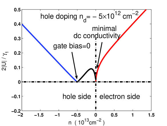
For the small gap, , we obtain different results for the electron and hole types of conductivity. For instance, if the bilayer contains acceptors (see Fig. 4) with concentration , the gap decreases linearly with the hole concentration and vanishes, when the gate bias is not applied and the hole concentration equals . Starting from this point, the gap increases and, thereafter, becomes again small (equal to zero in Fig. 4) at the carrier concentration corresponding to the minimal value of the dc conductivity. Therefore, the difference observed in Ref. MLS between these two values of carrier concentrations, at the zero bias and at the minimal conductivity, gives directly the donor/acceptor concentration in the bilayer. Then, for the gate bias applied in order to increase the electron concentration, the gap is rapidly opening with the electron appearance.
We see, that the asymmetry arises between the electron and hole sides of the gate bias. This asymmetry can simulate a result of the hopping integral in the electron spectrum CNM . In order to obtain the gap dependence for the case of electron doping, , the reflection transformation has to be made in Fig. 4.
The gap in the vicinity of the minimal conductivity point reaches indeed a finite value due to several reasons. One of them is the form of the ”mexican hat” shown in Fig. 2. Second, the trigonal warping is substantial at low carrier concentrations. Finally, the graphene electron spectrum is unstable with respect to the Coulomb interaction at the low momentum values. For the graphene monolayer as shown in Ref. Mi , the logarithmic corrections appear at the small momentum. In the case of the bilayer, the electron self-energy contains the linear corrections, as can be found using the perturbation theory. The similar linear terms resulting in a nematic order were also obtained in the framework of the renormalization group VY .
In conclusions, the gap opening in the gated graphene bilayer has an intriguing behavior as a function of carrier concentration. In the presence of the external doping charge, i. e. donors or acceptors, this function is asymmetric on the hole and electron sides of the gate bias and it is linear only for the large gate bias.
This work was supported by the Russian Foundation for Basic Research (grant No. 07-02-00571). The author is grateful to the Max Planck Institute for the Physics of Complex Systems for hospitality in Dresden.
References
- (1) E. McCann, V.I. Fal’ko, Phys. Rev. Lett. 96, 086805 (2006).
- (2) T. Ohta, A. Bostwick, T Seyller, K. Horn, and E. Rotenberg, Science 313, 951 (2006).
- (3) L.M. Zhang, Z.Q. Li, D.N. Basov, M.M. Foger, Z. Hao, and M.C. Martin, Phys. Rev. B 78, 235408 (2008).
- (4) A.B. Kuzmenko, E. van Heumen, D. van der Marel, P. Lerch, P. Blake, K.S. Novoselov, A.K. Geim, Phys. Rev. B 79, 115441 (2009).
- (5) Z.Q. Li, E.A. Henriksen, Z. Jiang, Z. Hao, M.C. Martin, P. Kim, H.L. Stormer, and D.N. Basov, Phys. Rev. Lett. 102, 037403 (2009).
- (6) E.V. Castro, K.S. Novoselov. S.V. Morozov, N.M.R. Peres, J.M.B. Lopes dos Santos, Johan Nilsson, F. Guinea, A.K. Geim, and A.H. Castro Neto, Phys. Rev. Lett. 99, 216802 (2007).
- (7) E.J. Nicol, J.P. Carbotte, Phys. Rev. B 77, 155409 (2008).
- (8) E. McCann, Phys. Rev. B 74, 161403(R) (2006).
- (9) E. McCann, D.S.L. Abergel, V.I. Fal’ko, Sol. St. Comm. 143, 110 (2007).
- (10) P. Gava, M. Lazzeri, A.M. Saitta, and F. Mauri, arXiv:0902.4615 (2009).
- (11) J.C. Slonchewski and P.R. Weiss, Phys. Rev. 109, 272 (1958).
- (12) J.W. McClure, Phys. Rev. 108, 612 (1957).
- (13) B. Partoens, F.M. Peeters, Phys. Rev. B 74, 075404 (2006).
- (14) E.V. Castro, K.S. Novoselov. S.V. Morozov, N.M.R. Peres, J.M.B. Lopes dos Santos, Johan Nilsson, F. Guinea, A.K. Geim, and A.H. Castro Neto, arXiv:0807.3348 (2008).
- (15) K.F. Mak, C.H. Lui, J. Shan, and T.F. Heinz, (2009).
- (16) E.G. Mishchenko, Phys. Rev. Lett. 98, 216801 (2007).
- (17) O. Vafek and K. Yang, arXiv:0906.2483 (2009).