The Fundamental Asymmetry in Interfacial Electronic Reconstruction between Insulating Oxides
Abstract
We present an ab initio study of the (001) interfaces between two insulating perovskites, the polar LaAlO3 and the non-polar SrTiO3. We observe an insulating-to-metallic transition above a critical LaAlO3 thickness. We explain that the high conductivity observed at the TiO2/LaO interface, and the lack of similar conductivity at the SrO/AlO2 interface, are inherent in the atomic geometry of the system. A large interfacial hopping matrix element between cations causes the formation of a bound electron state at the TiO2/LaO interface. This novel mechanism for the formation of interfacial bound states suggests a robust means for tuning conductivities at various oxide heterointerfaces.
A wide variety of novel physical phenomena are observed at the hetero-epitaxial interfaces between perovskite oxides 1 , such as high conductivity 3 ; 4 , external field doping 5 ; 6 , magnetism 7 and supercoductivity 8 , all of which are lacking in the bulk constituents. Understanding the rich physics of these systems, and their potential applications, has been the focus of intensive research in the past decade.
Recently, the discovery of many novel properties at the (001) epitaxial interface LaAlO3/SrTiO3 (LAO/STO) has boosted considerable research 4 ; 5 ; 6 ; 7 ; 8 ; 9 ; 10 ; 11 ; 12 . Since both LAO and STO are perovskite oxides, two types of interfaces can form along the (001) direction: TiO2/LaO (-type) and SrO/AlO2 (-type) 4 ; 9 . While experiments have found that the -type interface is insulating, a high-mobility quasi two-dimensional electron gas (Q2-DEG) is formed at the -type interface 4 when the LAO thickness exceeds a critical separation 5 ; 10 . The origin of the Q2-DEG is the key to understanding the novelty of the LAO/STO interface, but it is still under heated debate in both theory 13 ; 14 ; 15 ; 16 ; 17 ; 18 ; 19 ; 20 ; 21 and experiment 9 ; 22 ; 23 ; 24 ; 25 .
Broadly, there are two representative schools of thought. The first suggests an intrinsic mechanism due to the polar discontinuity at the interface 4 ; 9 . Since the nominal charges of the LaO and AlO2 planes in (001) LAO are +1 and -1 (STO has neutral SrO and TiO2 layers), there is a macroscropic electric field through the LAO. The voltage across the LAO is approximately proportional to its thickness and diverges with increasing thickness. To avoid the divergence, half an electron(hole) per two-dimensional unit cell must transfer across the -type(-type) interface, respectively 4 ; 9 . Nevertheless, this symmetric description can not account for the drastic difference in electronic properties of the two interfaces. The second school of thought posits that extrinsic oxygen vacancies generated by the pulsed laser deposition create the dominating carriers responsible for the conductivity 9 ; 22 ; 23 ; 24 . However, both the existence of a lower limit in the carrier density of fully oxidized -type interfaces 25 and the insulating property of -type interfaces 4 ; 9 strongly suggest that a more fundamental intrinsic asymmetry exists in the electronic reconstruction 26 between these two interfaces. In this Letter we reveal a fundamental difference in the electronic reconstruction between -type and -type interfaces and propose that the atomic geometry accounts for the difference.
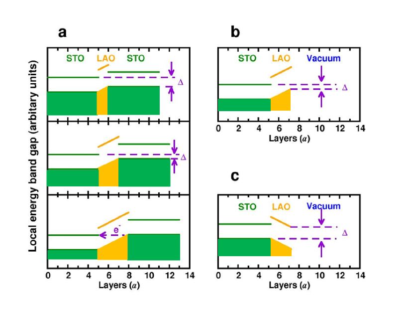
We begin by considering a schematic of the local energy gap in Fig. 1. We start with the simplest -type geometry in which several LAO layers are sandwiched between two thick slabs of STO with an -type interface on the left and a -type interface on the right. In both STO slabs, the local energy gap equals that of bulk STO (3.2 eV). For the LAO film it has the bulk LAO value (5.6 eV) except that the macroscopic electric field through the polar LAO lifts up its local energy gap, as illustrated in Fig. 1a. The energy gap of the entire interface system is thus determined by the difference between the conduction band edge (CBE) of STO on the left and the valence band edge (VBE) of STO on the right. Therefore, the LAO film serves to diminish the gap. As the LAO film thickens, the voltage across the LAO accrues until the VBE of STO on the right exceeds the CBE of STO on the left (bottom panel of Fig. 1a). At this point, the CBE on the left become more energically favorable than the VBE on the right and electrons transfer across the LAO. These transferred electrons reside on the Ti -orbitals of the CBE on the left while holes are left behind on the O -orbitals of the VBE on the right. This picture also applies to the -type interface (Fig. 1b) except that the holes stay in the O -orbitals of the LAO surface valence bands. For the -type interface (Fig. 1c), the polarity of the LAO film is reversed so the local band edges bend down, and the electron transfer occurs when the CBE of LAO is lower than the VBE of STO. In all three cases, the condition for electron transfer is that the voltage across the LAO film exceeds the band gap of STO (-type and -type) or the band gap of LAO (-type). The minimal LAO thickness satisfying this condition is the critical separation.
To verify and move beyond schematics, we employ density functional theory within the ab initio supercell plane-wave approach 27 with the local density approximation (LDA) 28 , and ultrasoft pseudopotentials 29 . All the super cells 33 in our simulation have the format (STO)/(LAO)l/(STO)/vacuum, in which are the numbers of STO unit cell and is that of LAO. could be half integers due to an extra atomic layer (i.e. half a unit cell). The vacuum separating periodic copies is Åin the (001) direction. For the -type and -type interfaces, is set to zero. For the -type, the interface between (STO) and (LAO)l is -type and that between (LAO)l and (STO) is -type. Typical values of and are 5 (for -type) and 11 (for -type and -type); is varied from 1 to 7. The interfaces are along (001) so the axis is perpendicular to the interfaces. The lengths in and directions of the unit cell, subject to periodic boundary conditions, are fixed to the theoretical lattice constant of STO Å(1.5% smaller than the experimental value). All atoms except two STO layers facing the surface 30 are fully relaxed in the direction until every force component is smaller than 26 meV/Å. The charge densities in Fig. 2 have been checked with convergence by reducing the force components to 13 meV/Å or smaller.
Our ab initio calculations support the above schematic view. For -type interfaces, once the transfer occurs, electrons accumulate at the interface and inhabit electronic states composed of Ti -orbitals in the STO; for a (001) growth direction, the states have clear character. For -type interfaces, holes inhabit states of pure O -character in the STO. Electron transfer occurs at 3, 4 and 5 LAO unit cells (u.c.) within DFT-LDA for -type, -type, and -type interfaces, respectively. Table 1 lists the energy gap versus the number of LAO u.c. as well as the corresponding potential change per added LAO u.c. Based on the data, extrapolates to 0.7 eV.
This potential change is predicted accurately by DFT as it is a ground-state property depending only on the electron density. However, since DFT describes excitations poorly, the computed STO and LAO band gaps are underestimated (1.85 and 3.25 eV, respectively) relative to experiments. Therefore, we use the experimental band gaps of STO and LAO to estimate the actual critical separation. The difference between the experimental and calculated band gaps is taken into account by adding extra LAO layers, each of which reduces the energy gap by 0.7 eV. Thus we predict experimental critical separations of 5, 6 and 8 LAO u.c. for -type, -type and -type interfaces, respectively 31 . The critical separation for the -type interface agrees very well with experiment 10 while our prediction for the -type interface (6 u.c.) is larger than the experimental value (4 u.c.) 5 . An important physical reason might be that we simulate perfectly flat, periodic, and defect-free LAO surfaces exposed to vacuum. In experiment, however, unavoidable imperfections of the surfaces (e.g. due to reconstructions or defects) may be responsible for an abrupt transition in the conductivities at smaller critical separation. For example, Cen et al. report that the creation and annihilation of oxygen vacancies at the surface could change the polar structure of the LAO film and the electronic properties of the interface 12 .
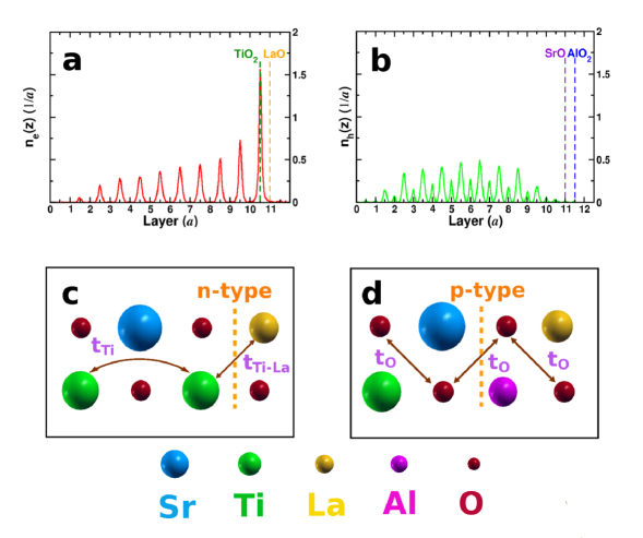
Our results also provide clear evidence of an asymmetry in the electronic reconstruction at -type and -type interfaces. Fig. 2a) and b) illustrate the -averaged spatial distribution of the transferred electron and hole densities along the (001) direction 32 . At the -type interface, the electron density decays monotonically into the STO, indicating a bound state. However, the holes are not bound to the -type interface because their density maximum is located in the middle of the STO substrate. (This feature persists as we thicken the STO.) This suggests that holes diffuse into the STO substrate while electrons stay close to the interface. Because carrier mobility depends on trapping and scattering, the asymmetry in these distributions provides a tentative explanation for the observed difference in conductivity at these two interfaces. Under an applied field in the -plane, electrons scatter only from defects within a few nanometers of the interface but the holes scatter off defects throughout the entire substrate. Given the high quality of the interface [9], electrons should be much more mobile than the holes. Furthermore, holes will easily be trapped on inevitable oxygen vacancies in the substrate which will further reduce their mobility.
There is a single experiment that infers the presence of oxygen vacancies per interfacial unit cell and attributes the insulating behavior of the -type interface to the vacancies 9 . However, our DFT calculations show that oxygen vacancies, just like holes, prefer to stay away from the -type interface 33 . Thus simulating a clean -type interface is certainly consistent theoretically. The discrepancy between experiment and theory needs to be resolved by additional experiments and theoretical calculations. Nevertheless, we agree that oxygen vacancies tend to trap and immobilize the hole carriers and thus render the -type interface insulating.
Then this begs the question: why are the electrons bound while the holes are not? Our answer hinges on topological asymmetry. The holes reside on O -orbitals and the oxygen atoms form a continuous network across the LAO/STO interface (Fig. 2d). We have calculated the hopping matrix elements between neighboring O -orbitals and found no significant discontinuity at the interface. Hence, the voltage across the polar LAO drives holes into the STO, but once there, they delocalize into the substrate.
However, the situation is very different for electrons. In STO and LAO, the conduction band edge states reside on the Ti and La cations, respectively. The Ti occupies the site in STO while in LAO the La occupies the site (in the standard nomenclature for perovskites), resulting in a discontinuity in the arrangement of the electronically active transition metals across the -type interface (Fig. 2c). A detailed examination shows that the electrons occupy mainly the Ti -orbitals but have a small weight on the La -orbitals in the first LaO layer at the interface. We calculate that the interfacial hopping matrix element between Ti -orbitals in the TiO2 plane and the La -orbitals in the LaO layer (Fig. 2c), which does not exist in either bulk oxide and is unique to the interface, is 0.7 eV, about 100 times larger than that between neighboring Ti -orbitals in STO. Two factors make this hopping so large: first, La 5-orbitals are spatially more extended than Ti 3-orbitals, and second, the distance between the La and Ti is of the Ti-Ti distance in bulk STO.
Thus, as a zeroth order approximation, we focus only on the interacting Ti and La at the interface. The strong interfacial hopping causes the Ti state to lower its energy and the La energy to rise. In chemical language, we form a pair of bonding and anti-bonding states between the two cations across the interface. Therefore, compared to the other Ti -orbitals in the substrate, the Ti -orbitals at the -type interface are more energetically favorable and bind electrons to the interface.
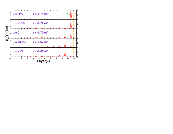
First principle simulations provide complete control over the system and allow us to verify the above picture via a gedanken experiment. We take the optimized (relaxed) -type interface structure as the reference. We manually move only the Ti atom at the interface by an amount , allow the electronic system to achieve self-consistency, and calculate the new interfacial properties including the hopping matrix element . When , the Ti atom moves away from the interface, the Ti-La bond is elongated and is weakened. When , the Ti atom moves towards the interface, shortens the La-Ti bond and strengthens . Fig. 3 shows how the transferred electron density responds to changing . As the Ti moves toward the interface, the electron density further localizes on the first Ti atom at the interface. When the Ti moves away, the biggest peak in the density profile then appears on the next Ti atom away from the interface. These results provide strong direct evidence that the large interfacial hopping between Ti - and La -orbitals traps and binds the electrons close to the interface.
In conclusion, we reveal a fundamental asymmetry in the electronic reconstruction at the -type and -type LAO/STO interface, which is accounted for by a strongly enhanced electronic hopping between the interfacial cations that host the carriers. This mechanism opens a pathway to nanoengineering electronic states at heterointerfaces. For example, doping different cations at the -type interface would change the spatial extent of atomic orbitals, modify the hopping element and thus tune the binding of the electrons to the interface. Mechanically, cation motions relative to the interface, e.g. by a ferroelectric or pieozoelectric effect, could similarly modify the distribution of the interfacial electron states.
We are grateful to Charles H. Ahn, Frederick J. Walker, Victor E. Henrich, Eric I. Altman and John C. Tully for stimulating discussions. This work was supported by the National Science Foundation under Contract No. MRSEC DMR 0520495. The Bulldog parallel clusters of the Yale High Performance Computing center provided computational resources.
References
- (1) S. B. Ogale, Thin Films and Heterostructures for Oxide Electronics (Springer Verlag, Berlin, 2005)
- (2) E. Dagotto, Science 318, 1076 (2007)
- (3) A. Ohtomo, D. A. Muller, J. L. Grazul and H. Y. Hwang, Nature 419, 378 (2002)
- (4) A. Ohtomo and H. Y. Hwang, Nature 427, 423 (2004)
- (5) S. Thiel, G. Hammerl, A. Schmehl, C. W. Schneider, J. Mannhart, Science 313, 1942 (2006)
- (6) H. Y. Hwang, Science 313 1895 (2006)
- (7) A. Brinkman, M. Huijben, M. Van Zalk, J. Huijben, U. Zeitler, J. C. Maan, W. G. Van der Wiel, G. Rijnders, D. H. A. Blank and H. Hilgenkamp, Nature Mater. 6, 493 (2007)
- (8) N. Reyren, S. Thiel, A. D. Caviglia, L. Fitting Kourkoutis, G. Hammerl, C. Ricther, C. W. Schneider, T. Kopp, A. S. Rüetschi, D. Jaccard, M. Gabay, D. A. Muller, J. M. Triscone, J. Mannhart, Science 317, 1196 (2007)
- (9) N. Nakagawa, H. Y. Hwang and D. A. Muller, Nature Mater. 5, 204 (2006)
- (10) M. Huijben, G. Rijnders, D. H. A. Blank, S. Bals, S. Van Aert, J. Verbeeck, G. Van Tendeloo, A. Brinkman and H. Hilgenkamp, Nature Mater. 5, 556 (2006)
- (11) P. R. Willmott, S. A. Pauli, R. Herger, C. M. Schlepütz, D. Martoccia, B. D. Patterson, B. Delley, R. Clarke, D. Kumah, C. Cionca and Y. Yacoby, Phys. Rev. Lett. 99, 155502 (2007)
- (12) C. Cen, S. Thiel, G. Hammerl, C. W. Schneider, K. E. Andersen, C. S. Hellberg, J. Mannhart and J. Levy, Nature Mater. 7, 298 (2008)
- (13) R. Pentcheva and W. E. Pickett, Phys. Rev. B 74, 035112 (2006)
- (14) M. S. Park, S. H. Rhim and A. J. Freeman, Phys. Rev. B 74, 205416 (2006)
- (15) J. M. Albina, M. Mrovec, B.Meyer, and C. Elsässer, Phys. Rev. B 76, 165103 (2007)
- (16) S. Gemming, G. Seifert Acta Mater. 54, 4299 (2006)
- (17) K. Janicka, J. P. Velev and E. Y. Tsymbal, J. Appl. Phys. 103, 07B508 (2008)
- (18) Z. Zhong and P. J. Kelly, Europhys. Lett. 84 27001 (2008)
- (19) U. Schwingenschlögl and C. Schuster, Europhys. Lett. 81, 17007 (2008)
- (20) Jaekwang Lee and Alexander A. Demkov, Phys. Rev. B 78, 193104 (2008)
- (21) R. Pentcheva and W. E. Pickett, Phys. Rev. B 78, 205106 (2008)
- (22) A. Kalabukhov, R. Gunnarsson, J. Börjesson, E. Olsson, T. Claeson and D. Winkler, Phys. Rev. B 75, 121404(R) (2007)
- (23) G. Herranz, M. Basletić, M. Bibes, C. Carrétéro, E. Tafra, E. Jacquet, K. Bouzehouane, C. Deranlot, A. Hamzić, J. M. Broto, A. Barthélémy, and A. Fert, Phys. Rev. Lett. 98, 216803 (2007)
- (24) W. Siemons, G. Koster, H. Yamamoto, W. A. Harrison, G. Lucovsky, T. H. Geballe, D. H. A. Blank, and M. R. Beasley, Phys. Rev. Lett. 98, 196802 (2007)
- (25) J. N. Eckstein, Nature Mater. 6, 473 (2007)
- (26) S. Okamoto and A. J. Millis, Nature 428, 630 (2004)
- (27) M. C. Payne, M. P. Teter, D. C. Allan, T. A. Arias, J. D. Joannopoulos, Rev. Mod. Phys. 64, 1045 (1992)
- (28) W. Kohn and L. J. Sham, Phys. Rev. 140, A1133 (1965)
- (29) D. Vanderbilt, Phys. Rev. B 41 7892 (1990)
- (30) The STO slabs in our simulations are always terminated in a SrO plane to avoid surface effects, as described in the EPAPS Document No. XXX.
- (31) The reason that the critical separation for -type interfacesis larger than that for -type is that the potential change by the first two unit cells of LAO (0.14 and 0.43 eV) are well below the extrapolated value 0.7 eV (See Table 1).
- (32) To be clear, the electron density (for -type interface) in Fig. 2a is the weighted sum of all the occupied states in the STO conduction bands and the hole density (for -type interface) in Fig. 2b is the weighted sum of all the unoccupied states in the STO valence bands.
- (33) See the EPAPS Document No. XXX for details.
| -type | -type | -type | ||||||
|---|---|---|---|---|---|---|---|---|
| (eV) | (eV) | (eV) | (eV) | (eV) | (eV) | |||
| 0 | 1.85 | 0 | 1.85 | 0 | 1.85 | |||
| 1 | 1.25 | 0.60 | 1 | 1.71 | 0.14 | 1 | 1.79 | 0.61 |
| 2 | 0.55 | 0.70 | 2 | 1.28 | 0.43 | 2 | 1.82 | 0.72 |
| 3 | metallic | 3 | 0.57 | 0.71 | 3 | 1.18 | 0.72 | |
| 4 | metallic | 4 | 0.49 | 0.69 | ||||
| 5 | metallic |