Shot noise and conductivity at high bias in bilayer graphene:
Signatures of electron-optical phonon coupling
Abstract
We have studied electronic conductivity and shot noise of bilayer graphene (BLG) sheets at high bias voltages and low bath temperature K. As a function of bias, we find initially an increase of the differential conductivity, which we attribute to self-heating. At higher bias, the conductivity saturates and even decreases due to backscattering from optical phonons. The electron-phonon interactions are also responsible for the decay of the Fano factor at bias voltages V. The high bias electronic temperature has been calculated from shot noise measurements, and it goes up to K at V. Using the theoretical temperature dependence of BLG conductivity, we extract an effective electron-optical phonon scattering time . In a 230 nm long BLG sample of mobility cm2V-1s-1, we find that decreases with increasing voltage and is close to the charged impurity scattering time fs at V.
I Introduction
Graphene, a two-dimensional plane of carbon atoms arranged in a honeycomb lattice, has recently attracted wide attention due to its unique properties. CastroNeto2009 High electronic mobility Bolotin2008 up to more than cm2 V-1 s-1 combined with a good scalability makes graphene-based field-effect transistors (FETs) potential basic building blocks for future nanoelectronics devices. A large on/off current ratio is required to challenge the current Si-based FETs. In monolayer graphene (MLG), the on/off current ratio is low (5) because the conductivity always remains above a value of roughly or for diffusive and ballistic miao2007 ; Danneau2008 samples, respectively. In bilayer graphene (BLG), this ratio can amount up to 20 000 thanks to the possibility to induce a band gap controlled by chemical doping Otah2006 or by a perpendicular electric field. Oostinga2008 ; Xia2010 ; Jing2010 The standard FETs commonly work at high bias voltage where electron-phonon interactions play a major role in the electronic transport. As a consequence, better knowledge of the electronic interactions in BLG is of importance for optimizing graphene-based nanoelectronics devices.
The electronic mobility of BLG samples supported on SiO2 does not exceed 10 000 cm2V-1s-1 due to a strong long-range scattering from charged impurities. Morozov2008 ; adam2008 ; Xiao2010 In suspended Feldman2009 or boron-nitride-supported Dean2010 ; DasSarma2011 BLG samples of higher mobility, the charged impurities scattering is much weaker and the short-range scattering (potentially caused by point defects, neutral scatterers or vacancies) is of importance. We consider here the low temperature limit ( K) where the electron-phonon coupling is negligible in the linear response regime. Adam2010 ; Viljas2010 With increasing bias voltage, the BLG differential conductivity in our samples initially goes up as a result of self-heating. Viljas2011 At high bias voltages, electron-optical phonon coupling is relevant and considerably influences the electronic transport. In MLG samples, partial current saturation was reported and related to electron-optical phonon (e-op) coupling. Meric2008 ; Barreiro2009 ; Perebeinos2010 ; Bae2010 This coupling was confirmed by investigating the phonon temperature by Raman spectroscopy. Chae2010 ; Berciaud2010 ; Freitag2010 In supported samples, the population of the different optical phonon modes is difficult to quantify partly because both the intrinsic optical phonons of the graphene and those of the SiO2 surface can be involved.
In this work, we present electronic conductance and shot noise measurements on several BLG samples. At high bias voltage, the decrease of both the conductance and the Fano factor are interpreted as signatures of electron-optical phonon coupling in BLG. The absence of current saturation is consistent with this coupling being weaker compared to that in MLG as calculated by Borysenko et al. Borysenko2011 Nevertheless, in this regime we may expect either the electron-phonon or electron-electron interactions to be strong enough for establishing a quasi-equilibrium electron energy distribution, and consequently an estimate of the effective electronic temperature can directly be extracted from shot noise. Santavicca2010 ; Wu2010 In this way, we find that the electronic temperature of our BLG samples can go up to K at a voltage of 0.75 V which confirms strong self-heating Viljas2011 and which agrees with optical spectroscopy experiments. Bae2010 Finally, we make use of the electronic temperature to extract an approximate for the e-op interaction time (). We find that this inelastic interaction time decreases with bias voltage becoming close to the elastic interaction time (60 fs) at a voltage of 0.6 V in a 230 nm long BLG sample.
II Sample fabrication and experimental setup
The BLG samples have been mechanically exfoliated from graphite by means of a semiconductor wafer dicing tape. A strongly doped Si substrate, separated by or nm of SiO2 from the sample, was used as a back-gate to tune the BLG charge density . The leads were patterned using standard e-beam lithography techniques and a bilayer resist was employed to facilitate the lift-off. The samples were contacted using Ti/Al/Ti sandwich structures with thicknesses 10 nm / / 5 nm where was varied over nm (10 nm of Ti is the contact layer). Metal evaporation was made in a ultra high vacuum chamber ( mBar) in order to obtain the highest contact transparency. note_contacts Samples of various lengths from 230 nm up to 1 and widths from 0.9 to 1.6 m were fabricated. All the data were measured using a two-lead configuration in a 4He dewar at a bath temperature of K.
Differential AC-conductivity was recorded at frequency Hz with a standard lock-in technique. The average Fano factor was calculated by integrating the current spectral density over the frequency range MHz. The noise generated by the sample was successively amplified by means of a home-made low-noise amplifier Roschier2004 at 4 K and room-temperature amplifiers by 16 dB and 70 dB, respectively. The 4He dewar was placed in a shielded room in order to protect noise measurements against external microwave radiation. After the two amplification stages, the noise was filtered with a band-pass filter ( MHz) and rectified using a Schottky diode. Danneau2008 At low noise power ( mW), the DC-voltage measured after the diode is directly proportional to the noise power. The noise calibration was done by measuring the shot noise of a tunnel junction which is known to have a Fano factor (see Ref. blanter2000, ). A microwave switch allowed us to use the same amplification channel for measuring the noise of the graphene sample and the tunnel junction. Danneau2008
III Introduction to shot noise
In mesoscopic devices, shot noise originates from the granular nature of charge carriers. Shot noise contains information on the electronic transport properties that can not be obtained by simple conductance measurements. blanter2000 Moreover, shot noise can be used to probe the electronic temperature of mesoscopic systems and it is even possible to use this effect as a primary thermometer. spietz03 At the zero frequency limit, shot noise is given by the correlation function of current fluctuations : . Typically, the strength of shot noise is characterized by the Fano factor, defined as . The measured average Fano factor is approximately related to the true Fano factor via the Khlus formula: Khlus87
| (1) |
Note that when , the measured is close to the true Fano factor (). The Fano factor is different depending on the considered mesoscopic sample. For example, it is for a low-transparency tunnel junction, for a diffusive metallic wire steinbach1996 ; henny1999 , for a chaotic cavity Brouwer1996 ; oberholzer2001 ; oberholzer2002 ; silvestrov2003 , and for a ballistic sample. reznikov1995 ; kumar1996 The shot noise measurements were used to measure the effective charge of in the fractional quantum Hall regime Saminadayar1997 ; depiciotto1997 and in a SN junction. Jehl2000 ; Kozhevnikov2000 It could also be used to study many-body interactions and spin related phenomena. roche2004 ; dicarlo2006 Shot noise has turned out to be very useful in the studies of graphene. Danneau2008 ; dicarlo2008 For ballistic bilayer graphene, theoretical calculations give either snyman2007 or ,katsnelson2006a i.e. very close to what has been observed at the charge neutrality point (CNP) in monolayers Danneau2008 ; dicarlo2008 and to the value for diffusive conductors without inelastic interactions. blanter2000 By reducing the width of MLG sheets down to nanoribbons, a strong suppression of shot noise has been observed consistent with inelastic hopping in these disordered systems. danneau2010
If local temperature is well defined (quasiequilibrium) at every position along the length of the graphene sheet, then it can be shown using theory for diffusive conductors that (for ) nagaev1995 ; naveh1998
| (2) |
where is the average temperature. footnote1 The electron-electron (e-e) interactions may lead to an increase of over the value .nagaev1995 This happens if the power carried away via e-op coupling is small, such that all the injected power goes to the leads. Then , i.e. , the “hot electron” value.blanter2000 Now, if heat leaks out from the system also via electron-optical phonon (e-op) coupling, then is reduced and hence decreases. Thus, there are two opposite tendencies for , but at very large bias the e-op coupling will dominate and reduce the noise.
IV Experimental results
In this paper, we focus on the results obtained on three different BLG samples. The first one is a 0.23 m long and 1.1 m wide BLG sample shown in the lower inset of Fig. 1. This sample located in between terminals H3 and H4 is named H in the following. We report also conductance measurements on two other samples of different length (0.35 m and 0.95 m) which have been built from the same BLG sheet (see lower left inset of Fig. 3). Experimental findings reported on these samples are qualitatively similar to those found on all the other measured BLG samples.
IV.1 Electronic mobility
In this section, we extract the electronic mobility of sample H which will be used later in Sec. V to calculate the theoretical BLG conductivity. Fig. 1 presents the gate voltage dependence of the zero-bias conductivity of sample H at 4.2 K. The conductivity is minimal and equal to 6.9 at the so-called charge neutrality point at V. This sample is thus -doped in the absence of a gate voltage. The gate voltage axis in Fig. 1 has been renormalized such that . In other BLG samples, we commonly observed an asymmetry between the zero-bias conductance in the - and -regions, the conductivity being lower in the -region. This asymmetry is more pronounced in short samples and probably originates from the -doping by the leads Khomyakov2010 and the ensuing formation of a - junction close to the contact-graphene interface when BLG is -doped Viljas2011 ; Huard2008 ; Barraza-Lopez2010 ; Khomyakov2010 ; Lee2008 ; Mueller2009 (). The -doped region has not been measured for sample H because of a strong initial -doping by impurities and the leads. The dashed line in Fig. 1 corresponds to the zero-bias conductance fit using the (zero-temperature) empirical relation , where is the “residual“ density and the mobility. In the parallel plate model, the charge density is related to the gate voltage via , with the gate capacitance per area. In short samples, the screening of the electric field by the leads decreases the effective gate capacitance. This modification can be accounted for in the parallel-plate model by replacing by a lower effective dielectric constant . By solving the Poisson equation, footnote2 we find and aF/m2.
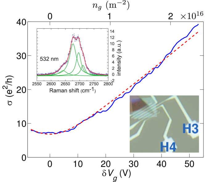
Using this gate capacitance value, we extract the mobility cm2V-1s-1 and the residual density m-2. In BLG, the impurity density is related to the mobility via the relation Viljas2011 , which gives m-2.
IV.2 Bias voltage dependence of BLG conductivity
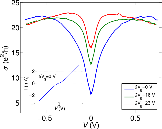
The bias voltage dependence of the differential conductivity of sample H is shown in Fig. 2 for three different gate voltages. At low bias, the conductivity increases linearly with voltage, leading to a superlinear current-voltage [] characteristic. This non-linearity is specific to bilayer graphene and does not show up in monolayer graphene (MLG). It has been explained in Ref. Viljas2011, by self-heating, though other contributions cannot be excluded in the case of this sample. Indeed, the conductivity in BLG is more sensitive to temperature than in MLG due to a higher density of states. adam2008 Above 0.1 V, the BLG conductivity grows slower and slower as the voltage increases, and reaches a maximum at V V. Above this voltage the conductivity begins to slowly decrease.
We also investigated the transport properties of 2 BLG samples of different length (350 nm and 950 nm) made from the same BLG sheet. Viljas2011 As shown in Fig. 3, at low bias and for the same charge density, the conductivity does not depend on the length of the sample, showing the same initial increase with voltage. However at higher bias, the conductivity of the short sample reaches a maximum and then decreases faster than in the long sample. We define as the voltage above which the conductivities of the short and long samples deviate.
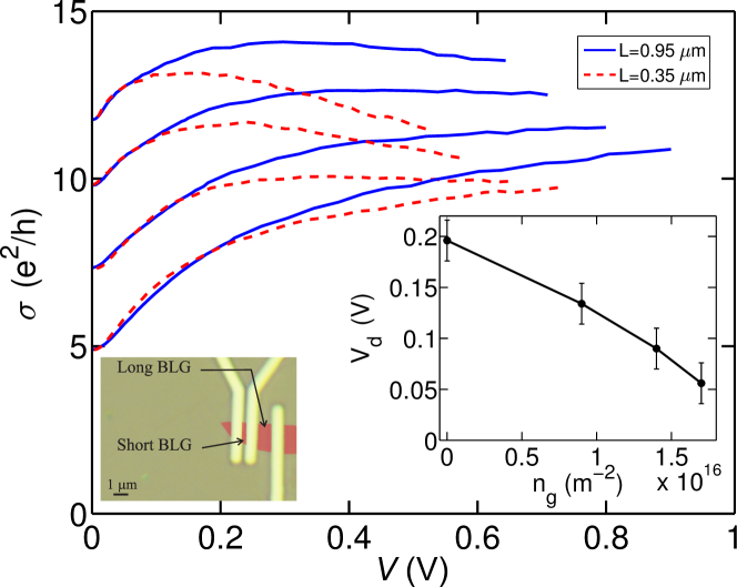
In order to explain these experimental results, we now focus on the backscattering induced by interactions between electrons and optical phonons (op). Note that extrinsic surface phonons modes of the SiO2 substrate are here relevant and may be the primary source of energy relaxation. Chen2008 ; Fratini2008 . In a simple model, we assume that the electrons are accelerated by the external electric field , so the energy gained by the electron after a distance is . When this energy reaches the characteristic optical phonon energy , electrons can transmit their energy to optical phonons (op). Assuming an instantaneous energy exchange, the “threshold” mean-free-path for the onset of scattering is thus given by Yao2000 . At the same bias voltage, the electric field is higher in the short sample and, consequently, the threshold mean free path is shorter. This explains why the conductivity of the short sample is lower than that of the long sample. At low bias voltages, the fact that the conductivities of both samples are almost identical is in agreement with a self-heating effect Viljas2011 in absence of electron-phonon coupling. The voltage is lowered when the charge density increases [inset of Fig. 3], suggesting an enhancement of backscattering from phonons far from the CNP.
IV.3 Shot noise in BLG
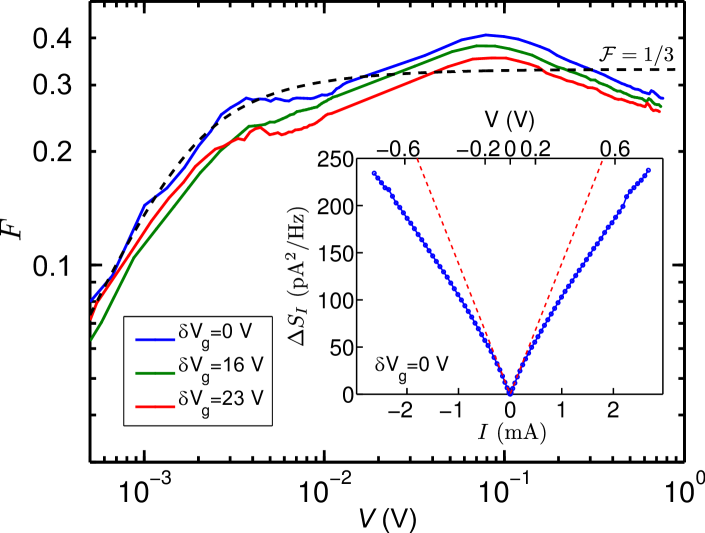
Additional information to electronic conductivity measurements was obtained from shot noise in BLG. In particular, an effective electronic temperature was directly obtained from shot noise, which is analyzed in Sec. V.2 to extract an estimate for the e-op interaction time. Fig. 4 presents the voltage dependence of the average Fano factor for the same gate voltages as for the conductivity curves in Fig. 2. At low bias voltages mV, increases linearly with voltage as expected from the Khlus formula (1) when : . By fitting the noise at low bias with the Khlus formula with a fixed temperature K, we find that is close to at the CNP as expected for a diffusive sample, blanter2000 and it is slightly lower far from the CNP which may be related to disorder SanJose2007 ; Tworzydlo2008 ; Lewenkopf2008 ; Titov2010 ( at and V.). At bias voltages above 20 mV, the average Fano factor is weakly dependent on gate voltage, and first goes higher than predicted from the Khlus formula. We interpret this as a signature of a hot-electron regime. steinbach1996 Above 0.1 V, decays and goes to a value of at V. We assign the decrease of the Fano factor at high bias voltages to the coupling between electrons and optical phonons.
V Electron-optical phonon scattering time
The theoretical conductivity for BLG is a function of the chemical potential , the average electronic temperature and the electron scattering time , which is independent of energy for screened Coulomb impurities. Viljas2011 Introducing again the phenomenological residual density , we may write the conductivity as
| (3) |
with and the electron and hole concentrations, respectively. The chemical potential is related to the charge density via the relation . We assume that electron and hole mobilities are identical Viljas2011 and given by . Using Matthiessen’s rule, we simply replace the scattering rate by the sum of two contributions: , coming from charged impurity and electron-phonon scattering, respectively. At zero bias, charged impurity scattering dominates, Adam2010 ; Viljas2010 so . Using the zero bias mobility cm2V-1s-1, we deduce fs. We assume next that does not depend on voltage.
In the following, we first consider only scattering from charged impurities, neglecting inelastic processes, i.e. . In order to calculate the conductivity from Eq. (3), the electronic temperature () has to be known. In the next section, is extracted at low bias by solving the heat diffusion equation in absence of electron-phonon coupling and at high bias from shot noise measurements (in presence of e-op coupling).
V.1 Electronic temperature
As shown in Sec. IV.2, at low bias voltage the electron-phonon interactions can be neglected. Under this condition, assuming that the electron energy distribution function is at quasi-equilibrium, the electronic temperature at the position along the BLG sheet is given by solving the heat diffusion equation, using the Wiedemann-Franz law. In the limit where K, it yields
| (4) |
where is the Lorenz number. The average temperature increases linearly with and it goes up to 250 K at V [see dashed line in Fig. 5].
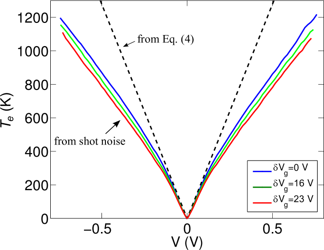
Above V, electrons interact with optical phonons, and thus the average temperature calculated from Eq. (4) is an overestimate. In this inelastic interaction regime, the electronic temperature can be extracted from the Fano factor using Eq. (2). We find K at V which is much lower than the temperature of 2300 K we would observe without energy relaxation to phonons [dashed line in Fig. 5]. Note that the electronic temperature does not depend much on gate voltage at high bias. This can be understood from the fact that the broadening of the electron energy distribution () is much larger than the chemical potential .
V.2 Theoretical conductivity and electron-optical phonon scattering time
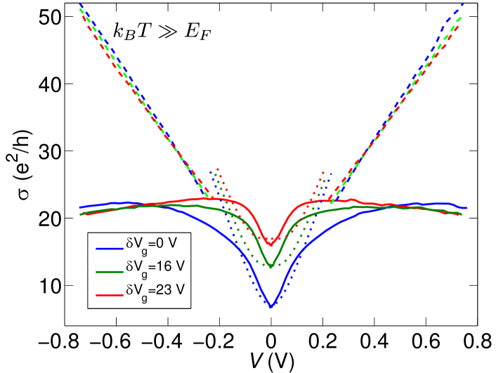
The dotted lines shown in Fig. 6 depict the theoretical conductivities at low bias as a function of voltage calculated without any free parameters by using Eq. (3) and the average temperature from Eq. (4). The theoretical conductivity does not change much at low bias and increases at higher bias linearly with voltage. This leads to a low bias conductivity “plateau” whose width grows with increasing the chemical potential . This conductivity plateau has not been observed in any of our measured BLG samples as discussed in Ref. Viljas2011, .
.
At high bias voltages ( V), by using the temperature extracted from the Fano factor, we find that the theoretical conductivity given by Eq. (3) increases linearly with increasing and is almost always above the experimental conductivity (dashed lines in Fig. 6). As a result, the discrepancy between the theoretical and experimental conductivities increases with increasing . This was to be expected as we have only considered so far charged impurity scattering and ignored e-op phonon interactions.
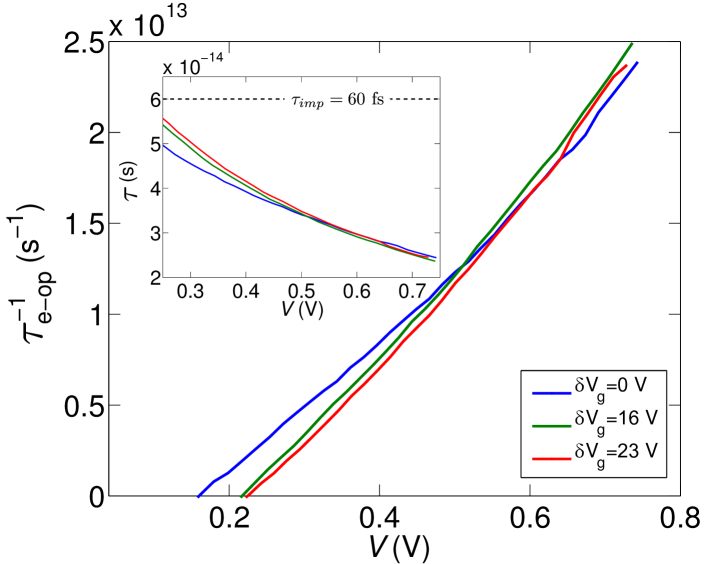
We next fit the experimental conductivity with Eq. (3) by adjusting the interaction time . Note that the temperature extracted from the Fano factor takes into account e-op interactions and, thus, is still valid. At V, the theoretical and experimental conductivities are close, resulting in a large uncertainty for . We find that the scattering rate does not depend much on gate voltage (Fig. 7). This can again be understood from the fact that . The rate is very low ( s-1) at voltages below V and charged impurity scattering dominates. Above V, increases almost linearly with increasing the bias voltage, as calculated for MLG. tse2008 At V, the inelastic rate is fs-1 which is close to fs-1. The increase of the inelastic scattering rate can be explained by the presence of more phase space for the e-op scattering.
VI Conclusion
In conclusion, we have investigated conductance and shot noise in several BLG samples at a bath temperature of 4.2 K. At low bias voltage, the increase of the differential conductivity with voltage is attributed to self-heating. In this regime, the scattering time is limited by charged impurity scattering. At high bias voltage, decrease in the conductance indicates electron-optical phonon scattering which is also confirmed by reduction of shot noise. The drop of the conductivity is more pronounced in short samples suggesting a larger e-op scattering rate. This agrees with the expectation that the threshold mean-free-path for e-op coupling is directly proportional to the sample length. At high bias voltage, the electronic temperature in the BLG sheet is deduced from shot noise measurements. The electronic temperature goes up to 1200 K at a voltage of V. From the temperature , we estimated the e-op scattering time and found that it decreases with increasing voltage. In a 230 nm long BLG sample, we find that goes below the elastic scattering time fs at a voltage of V. The e-op coupling is thus manifested at the standard working points of graphene-based FETs. Extended work on suspended graphene samples is of interest in order to suppress the relaxation channel to SiO2 surface phonons.
Aknowledgment
This work was supported by the Academy of Finland, the European Science Foundation (ESF) under EUROCORES Programme EuroGraphene and the EU project MMM@HPC FP7-261594. R.D.’s Shared Research Group SRG 1-33 received financial support by the Karlsruhe Institute of Technology within the framework of the German Excellence Initiative.
References
- (1) :
- (2) A. H. Castro Neto, F. Guinea, N. M. R. Peres, K. S. Novoselov, and A. K. Geim, Rev. Mod. Phys. 81, 109 (2009).
- (3) K. I. Bolotin, K. J. Sikes, Z. Jiang, M. Klima, G. Fudenberg, J. Hone, P. Kim, H. L. Stormer, Solid State Comm. 146, 351 (2008).
- (4) F. Miao, S. Wijeratne, Y. Zhang, U. C. Coskun, W. Bao, and C. N. Lau, Science 317, 1530 (2007).
- (5) R. Danneau, F. Wu, M. F. Craciun, S. Russo, M. Y. Tomi, J. Salmilehto, A. F. Morpurgo, and P. J. Hakonen, Phys. Rev. Lett. 100, 196802 (2008); J. Low Temp. Phys. 153, 374 (2008); Solid State Commun. 149, 1050 (2009).
- (6) T. Otah, A. Bostwick, T. Seyller, K. Horn, and. E. Rotenberg, Science 313, 951 (2006).
- (7) F. Xia, D. B. Farmer, Y.-M. Lin, and P. Avouris, Nano Lett. 10, 715 (2010).
- (8) L. Jing, J. Velasco Jr., P. Kratz, G. Liu, W. Bao, M. Bockrath, and C. N. Lau, Nano Lett. 10, 4000 (2010).
- (9) J. B. Oostinga, H. B. Heersche, X. Liu, A. F. Morpurgo, and L. M. K. Vandersypen, Nat. Mater. 7, 151 (2008).
- (10) S. Adam and S. D. Sarma, Phys. Rev. B 77, 115436 (2008).
- (11) S. V. Morozov, K. S. Novoselov, M. I. Katsnelson, F. Schedin, D. C. Elias, J. A. Jaszczak, and A. K. Geim, Phys. Rev. Lett. 100, 016602 (2008).
- (12) S. Xiao, J.-H. Chen, S. Adam, E. D. Williams, and M. Fuhrer, Phys. Rev. B 82, 041406 (2010).
- (13) B. E. Feldman, J. Martin, and A. Yacoby, Nature Phys. 5, 889 (2009).
- (14) C. R. Dean, A. F. Young, I. Meric, C. Lee, L. Wang, S. Sorgenfrei, K. Watanabe, T. Taniguchi, P. Kim, K. L. Shepard, and J. Hone, Nat. Nanotechnol. 5, 722 (2010).
- (15) S. Das Sarma and E. H. Hwang, Phys. Rev. B 83, 121405(R) (2011).
- (16) J. K. Viljas and T. T. Heikkilä, Phys. Rev. B 81, 245404 (2010).
- (17) S. Adam and M. D. Stiles, Phys. Rev. B 82, 075423 (2010).
- (18) J. K. Viljas, A. Fay, M. Wiesner, and P. J. Hakonen, Phys. Rev. B 83, 205421 (2011).
- (19) I. Meric, M. Y. Han, A. F. Young, B. Ozyilmaz, Ph. Kim, abd K. L. Shepard, Nat. Nanotechnol. 3, 654 (2008).
- (20) A. Barreiro, M. Lazzeri, J. Moser, F. Mauri, and A. Bachtold, Phys. Rev. Lett. 103, 076601 (2009).
- (21) V. Perebeinos and P. Avouris, Phys. Rev. B 81, 195442 (2010).
- (22) M.-H. Bae, Z.-Y. Ong, D. Estrada, and E. Pop, Nano Lett. 10, 4787 (2011).
- (23) M. Freitag, H.-Y. Chiu, M. Steiner, V. Perebeinos, and P. Avouris, Nature Nanotech. 5, 497 (2010).
- (24) D.-H. Chae, B. Krauss, K. von Klitzing and J. H. Smet, Nano Lett. 10, 466 (2010).
- (25) S. Berciaud, M. Y. Han, K. F. Mak, L. E. Brus, P. Kim, and Tony F. Heinz, Phys. Rev. Lett. 104, 227401 (2010).
- (26) K. M. Borysenko, J. T. Mullen, X. Li, Y. G. Semenov, J. M. Zavada, M. Buongiorno Nardelli, and K. W. Kim, Phys. Rev. B 83, 161402(R) (2011).
- (27) D. F. Santavicca, J. D. Chudow, D. E. Prober, M. S. Purewal, and P. Kim, Nano Lett. 10, 4538 (2010).
- (28) F. Wu, P. Virtanen, S. Andresen, B. Plaçais, and P. J. Hakonen, App. Phys. Lett. 97, 262115 (2010).
- (29) We have measured maximum contact resistances on the order of 20 .
- (30) L. Roschier and P. Hakonen, Cryogenics 44, 783 (2004).
- (31) Ya. M. Blanter, and M. Büttiker, Phys. Rep. 336, 1 (2000).
- (32) L. Spietz, K. W. Lehnert, I. Siddiqi, R. J. Schoelkopf, Science 300, 1909 (2003).
- (33) V. A. Khlus, Zh. Eksp. Teor. Fiz. 93, 2179 (1987) [Sov. Phys. JETP 66, 1243 (1987)].
- (34) A. H. Steinbach, J. M. Martinis, and M. H. Devoret, Phys. Rev. Lett. 76, 3806 (1996).
- (35) M. Henny, S. Oberholzer, C. Strunk, and C. Schönenberger, Phys. Rev. B 59, 2871 (1999).
- (36) P. W. Brouwer and C. W. J. Beenakker, J. Math. Phys. 37, 4904 (1996).
- (37) S. Oberholzer, E. V. Sukhorukov, C. Strunk, C. Schönenberger, T. Heinzel, and M. Holland, Phys. Rev. Lett. 86, 2114 (2001).
- (38) S. Oberholzer, E. V. Sukhorukov, and C. Schönenberger, Nature 415, 765 (2002).
- (39) P. G. Silvestrov, M. C. Goorden, and C. W. J. Beenakker, Phys. Rev. B 67, 241301(R) (2003).
- (40) M. Reznikov, M. Heiblum, H. Shtrikman, and D. Mahalu, Phys. Rev. Lett. 75, 3340 (1995).
- (41) A. Kumar, L. Saminadayar, D. C. Glattli, Y. Jin, and B. Etienne, Phys. Rev. Lett. 76, 2778 (1996).
- (42) L. Saminadayar, D. C. Glattli, Y. Jin, and B. Etienne, Phys. Rev. Lett. 79, 2526 (1997).
- (43) R. de-Picciotto, M. Reznikov, M. Heiblum, V. Umansky, G. Bunin, and D. Mahalu, Nature 389, 162 (1997).
- (44) X. Jehl, M. Sanquer, R. Calemczuk, and D. Mailly, Nature 405, 50 (2000).
- (45) A. A. Kozhevnikov, R. J. Schoelkopf, and D. E. Prober, Phys. Rev. Lett 84, 3398 (2000).
- (46) P. Roche, J. Ségala, D. C. Glattli, J. T. Nicholls, M. Pepper, A. C. Graham, K. J. Thomas, M. Y. Simmons, and D. A. Ritchie, Phys. Rev. Lett. 93, 116602 (2004).
- (47) L. DiCarlo, Y. Zhang, D. T. McClure, D. J. Reilly, C. M. Marcus, L. N. Pfeiffer, and K. W. West, Phys. Rev. Lett. 97, 036810 (2006).
- (48) L. Dicarlo, J. R. Williams, Y. Zhang, D. T. McClure, and C. M. Marcus, Phys. Rev. Lett. 100, 156801 (2008).
- (49) I. Snyman and C. W. J. Beenakker, Phys. Rev. B 75, 045322 (2007).
- (50) M. I. Katsnelson, Eur. Phys. J. B 52, 151 (2006).
- (51) R. Danneau, F. Wu, M. Y. Tomi, J. B. Oostinga, A. F. Morpurgo, and P. J. Hakonen, Phys. Rev. B 82, 161405(R) (2010).
- (52) K. E. Nagaev, Phys. Rev. B 52, 4740 (1995).
- (53) Y. Naveh, D. V. Averin, and K. K. Likharev, Phys. Rev. B 58, 15371 (1998).
- (54) Using Eq. (2) for graphene close to the CNP is an approximation, because the derivation of the result requires a constant density of states.
- (55) P. A. Khomyakov, A. A. Starikov, G. Brocks, and P. J. Kelly, Phys. Rev. B 82, 115437 (2010).
- (56) B. Huard, N. Stander, J. A. Sulpizio, and D. Goldhaber-Gordon, Phys. Rev. B 78, 121402 (2008).
- (57) S. Barraza-Lopez, M. Vanević, M. Kindermann, and M. Y. Chou, Phys. Rev. Lett. 104, 076807 (2010).
- (58) E. J. H. Lee, K. Balasubramanian, R. T. Weitz, M. Burghard, and K. Kern, Nature Nanotechnol. 3, 486 (2008).
- (59) T. Mueller, F. Xia, M. Freitag, J. Tsang, and Ph. Avouris, Phys. Rev. B 79, 245430 (2009).
- (60) The effective dielectric constant used in the parallel plate model is chosen to give the same average charge density than calculated by solving analytically the Poisson equation in Ref. Viljas2011, .
- (61) J.-H. Chen, C. Jang, S. Xiao, M. Ishigami, and M. S. Fuhrer, Nat. Nanotechnol. 3, 206 (2008).
- (62) S. Fratini and F. Guinea, Phys. Rev. B 77, 195415 (2008).
- (63) Z. Yao, C. L. Kane, and C. Dekker, Phys. Rev. Lett. 84, 2941 (2000).
- (64) P. San-Jose, E. Prada, and D. S. Golubev, Phys. Rev. B 76, 195445 (2007).
- (65) J. Tworzydło, C. W. Groth, and C. W. J. Beenakker, Phys. Rev. B 78, 235438 (2008).
- (66) C. H. Lewenkopf, E. R. Mucciolo, and A. H. Castro Neto, Phys. Rev. B 77, 081410(R) (2008).
- (67) M. Titov, P. M. Ostrovsky, I. V. Gornyi, A. Schuessler, and A. D. Mirlin, Phys. Rev. Lett. 104, 076802 (2010).
- (68) W.-K. Tse, E. H. Hwang, and S. D. Sarma, Appl. Phys. Lett. 93, 023128 (2008).