Quantum Bus of Metal Nanowire with Surface Plasmon Polaritons
Abstract
We develop an architecture for distributed quantum computation using quantum bus of plasmonic circuits and spin qubits in self-assembled quantum dots. Deterministic quantum gates between two distant spin qubits can be reached by using an adiabatic approach in which quantum dots couple with highly detuned plasmon modes in a metallic nanowire. Plasmonic quantum bus offers a robust and scalable platform for quantum optics experiments and the development of on-chip quantum networks composed of various quantum nodes, such as quantum dots, molecules and nanoparticles.
pacs:
03.67.-a, 32.80.-t, 42.50.Pq, 73.20.MfPlasmonic circuits, providing the ability to integrate electronics and optics on the nanoscale, may lead an exciting application to carry classical information between microprocessors in integrated chip Ozbay2006 . For a scalable quantum chip, it is also desired to find a high speed on-chip quantum bus where the information can be coherently transferred between distant processing nodes. Integrated plasmonic circuits are an attractive route towards realizing such promise since they allow for scalability and coherent coupling to single emitters Lukin2006PRL ; Lukin2007PRB ; Lukin2007Nature ; Lukin2007NP . Recently, self-assembled quantum dots are argued as a promising candidate for building a practical quantum processor for their potential advantages, including self-evident scaling, ultra-fast coherent control and long lived spin states Calarco ; Nazir ; Nazir2008 ; Machnikowshi . Picosecond optical coherence measurement, preparation and manipulation of electron spin states have been demonstrated in self-assembled quantum dot systems Awschalom2006 ; Imamoglu2007 ; Awschalom2007 . However, most of the proposals for coherent coupling of two spin qubits are based on the interactions between neighboring dots Sandoghdar2002 ; Imamoglu2008 . A solution is expected to utilize quantum bus to couple qubits in a non-local and switchable way. Here we show the implementation of a quantum bus, using the surface plasmon polaritons confined in the metallic nanowires, to coherently couple an arbitrary pair of distant semiconductor quantum dot spin qubits. The interaction is mediated by the exchange of virtual surface plasmon polaritons rather than real ones, avoiding the decoherence of the system. Using adiabatic control of the qubits, we demonstrate high fidelity quantum operations between spatially separated spin qubits. Our approach is applicable to a wide class of electronic spin qubits near the nanowire and can be used for the implementation of distributed quantum computing architectures.
Fig. 1 shows our scalable solid state quantum computer architecture, in which spins in self-assembled quantum dots (QDs) act as qubits. These QDs can be grown by molecular beam epitaxy along the axis. Single electron can be deterministically injected to QD by the semi-transparent metallic gate. Each QD is selectively coupled to a laser field guided by a nanotip and a fiber taper which has been realized in recent experiment Ren2009 . The coupling between QDs is mediated by surface plasmon modes in metallic nanowire. Throughout, we use a silver nanowire with electric permittivity at room temperature and a vacuum wavelength nm Kroner , and the surrounding dielectric (the nanowire is covered with a thin layer of PMMA). We assume a large oscillator strength QDs which corresponds lateral radius of around 22nm Peter . In the following, we discuss the quantization of surface plasmons in metal nanostructure and then give the detailed coupling mechanism between QD spin and plasmon.

Surface plasmons, or surface plasmon polaritons are generally treated as classical electromagnetic waves that propagate along surface of a conductor. Recent experiment has shown that the fluorescence of quantum dots can be coupled to metallic nanowires and single, quantized plasmon can be generated Lukin2007Nature . In this work, we present a fully quantum mechanical approach for the interaction between electron spin in QD and quantized plasmon in the nanowire. In a cylindrical nanowire, the solution to electromagnetic modes has been given in Ref. Arista2001 ; Arista2003 for quite some time. The energy of the surface plasmon field is the sum of the kinetic and electrostatic energy
| (1) |
where is the equilibrium electron density in the metal, is the electron mass, is the velocity potential, is the charge density displacement from equilibrium, and is the scalar potential at the surface. The velocity potential and electronic density displacement satisfies the continuity equation
| (2) |
For a cylindrical nanowire of radius and length , the velocity potential and electrical potential can be expanded in cylindrical coordinates
| (3) | |||||
| (4) |
and the electronic density is correspondingly expressed as
| (5) |
where and are the cylindrical Bessel functions. Applying Maxwell’s boundary conditions, the relations between the coefficients , , and can be determined. With the electromagnetic field quantization calculations Scully , the Hamiltonian of the surface plasmon field Eq. (1) can be expressed in the standard second quantized form
| (6) |
where , is the bulk plasma frequency, is the background dielectric constant of the silver, and .
We consider single-charged self-assembled QDs with strong confinement along the growth direction. Because of the large heavy-hole-light-hole splitting, we can neglect the light-hole excitons and the QD can be effectively described by a four-level system, the electron spin states , , and the two trion states consisting of two spin paired electrons and unpaired heavy hole, , . The qubit is encoded in spin states of the excess electron. The polarized light guided by a metallic nanotip can only connect spin state to an optically excited trion state as shown in Fig. 1(b). Using the rotating wave approximation, the Hamiltonian between the QD and circularly polarized laser is expressed as
| (7) |
Here is the optical Rabi amplitude due to laser field guided by nanotip, , is the trion energy, and is the laser frequency.
The interaction between the plasmon field and a QD is given by
| (8) |
where is dipole operator of QD, and is electric field of surface plasmon. In the nanowire limit () all higher order modes are cutoff, thus we only consider the fundamental mode (), in which longitudinal wave vector propagating along nanowire satisfies a specifical condition. The electric field component ( direction) vanishes for the fundamental mode Lukin2007PRB . It’s assumed that the electric field component (the radial direction) has the main contribution to spin quantum number () of surface plasmon Nakamura . Thus we use , where is the distance between QD and nanowire edge, , and , represent the unit vectors of circularly polarized light. If the longitudinal component of electric field ( direction) has contribution to spin angular momentum of surface plasmon, the following results will be obtained in a similar way. Therefore, the interaction Hamiltonian between the plasmon field and QDs in the rotating wave approximation in the basis is
| (9) |
where is the coupling strength between the QD and metal nanowire, , are the creation and annihilation operators for fundamental surface plasmon mode of the nanowire with a specifical wave vector , the detuning is . From the Eq. (8) and Eq. (9), the coupling strength between the nanowire and QD is found to be
| (10) |
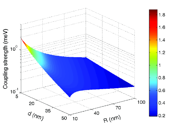
where , is electron charge, is the vacuum electric constant. The results of coupling strength against the nanowire radius and the distance between QD and nanowire edge with a nanowire length of m and a QD of exciton oscillator strength are shown in Fig. 2.
We have also carried out the detailed numerical simulations using the finite element method (FEM) to verify the analytical results above. We use FEM simulations to obtain the electromagnetic field solution and mode volume of nanowire. In the inset of Fig. 3, we plot the mode profile () of electric field () with a nanowire of nm and , where , and , denote the electric field outside and inside the nanowire respectively. The electromagnetic field presents the reflection and leakage at the end surface of nanowire as shown in the inset, which are not involved in the analytical model. The coupling strength of QD and nanowire interaction is given by Claudio , where is the plasmon mode volume (). The results of FEM simulations show meV for a nanowire of nm and nm, while the coupling constant is meV through Eq. (10). The analytical results are larger than the results given by FEM simulations because of the leakage of electromagnetic field at end surface. To neglect the affect of the leakage of electromagnetic field, we plot the normalized coupling strength /( nm, ) as a function of given by both FEM simulations and the analytical derivation respectively in Fig. 3. It is found that the FEM simulation results and analytical derivations agree closely.

The dynamics of the coupled system of QDs and nanowire can be described by the whole Hamiltonian:
| (11) |
describes the plasmon decay through Landau damping, while describes the coupling of QD to Markovian reservoirs. We consider several quantum dots coupled to a metallic nanowire and each dot is irradiated with an identical frequency polarized laser light. In the rotating frame at the laser frequency, the Hamiltonian is given by
| (12) |
where .
To explore the applications of the plasmonics based quantum bus, we consider the implementation of a controlled-phase (CPHASE) gate between two distant spin qubits (-th and -th qubits). The adiabatic control is applied to avoid the trion spontaneous emission and the plasmon decay. We use a laser pulse with slowly changing Gaussian field amplitude and a constant detuning. The evolution operator due to the adiabatic pulse is . Each phase change of the four computational basis states depends on adiabatic phase shift of single qubit and nonlinear phase shift of both qubits . Assume that the plasmon field is initially in the vacuum state. If the optical pulse of amplitude is large enough to create a gate phase Re, a gate locally equivalent to the CPHASE gate is achieved Zoller2001 . Up to a basis change of the target qubit and a phase shift on the control qubit, CPHASE gate is equivalent to controlled-not (CNOT) gate.
To estimate the performance of plasmonic quantum bus, we follow the standard quantum theory of damping to calculate CPHASE gate fidelity in Markovian approximation. The master equation for QDs and nanowire system can be described by
| (13) |
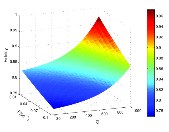
where is density matrix of two qubits and nanowire coupled system, , and describes the trion decay effect induced by various scattering channels such as phonon environment and radiation field. For self-assembled InGaAs QDs, the key decoherence parameter is trion radiative recombination time which is about ns. On the other hand, the effective lifetime of surface plasmon modes is , where is the decay rate of surface plasmon in nanowire. We consider two qubits initialized into the . Applying adiabatic Gaussian pulses with ) on both qubits, the output density matrix is following the master equation (13) after the gate. The fidelity is defined as , where the is the output density matrix following the master equation without decay terms. We calculated numerically the fidelity of CPHASE gate of two distant qubits versus the decay rate of the trion state and the quality factor of the plasmonic cavity with optimum and under the adiabatic approximation, as shown in Fig. 4. It is shown that, for ps-1 and , the fidelity of the two-qubit gate can be . The high-Q plasmonic microcavities () have been reported in recent experiment Vahala . Thus, high fidelity operations of two-qubit gate can be achieved between two separated spin qubits coupled via quantum bus of plasmon circuits.
We finally discuss potential realizations of distributed quantum computing architectures which are based on plasmon mediated nonlocal spin-spin interactions Hollenberg . In the hybrid platform, each node which consists of a nanowire and a few physical qubits, connects to a QD acting as a transceiver qubit and all the transceiver qubits are coupled via a plasmonic circuit or dielectric waveguide Lukin2007NP . A key technique to implement distributed quantum computing is performing a nonlocal CNOT gate between qubit A in the -th node and qubit B in the -th node. We firstly apply polarized laser pulses on both -th and -th transceiver qubits to prepare the qubits to be Einstein-Podolsky-Rosen state . After a set of sequential operations including CNOT gate between qubit A and -th transceiver qubit, CNOT gate between qubit B and -th transceiver qubit, single qubit measurement and operation Eisert , the nonlocal CNOT gate between qubit A and qubit B is completed.
In summary, we develop a novel and scalable method to controllably couple any distant electron spins in self-assembled quantum dots via surface plasmon based quantum bus. A fully quantum mechanical approach is introduced to describe the interaction between surface plasmon polariton of metal nanowire and quantum dot spins. Virtual plasmon excitation is exploited to overcome the decoherence of the system and a switchable long range interaction is achieved between spin qubits. The proposed architecture is an attractive approach for distributed quantum computation in a chip and realizable by the present standard solid state chip technology.
Acknowledgement This work was supported by the National Basic Research Program of China (Grants No. 2009CB929600, No. 2006CB921900), the National Natural Science Foundation of China (Grants No. 10804104, No. 10874163, No. 10604052) and the State Key Program of the National Natural Science Foundation of China (Grants No. 10934006).
References
- (1) E. Ozbay, Science 311, 189 (2006).
- (2) D. E. Chang, A. S. Soensen, P. R. Hemmer, and M. D. Lukin, Phys. Rev. Lett. 97, 053002 (2006).
- (3) D. E. Chang, A. S. Soensen, P. R. Hemmer, and M. D. Lukin, Phys. Rev. B 76, 035420 (2007).
- (4) A. V. Akimov, A. Mukherjee, C. L. Yu, D. E. Chang, A. S. Zibrov, P. R. Hemmer, H. Park, and M. D. Lukin, Nature 450, 402 (2007).
- (5) D. E. Chang, A. S. Soensen, E. A. Demler, and M. D. Lukin, Nature Phys. 3, 807 (2007).
- (6) T. Calarco, A. Datta, P. Fedichev, E. Pazy, and P. Zoller, Phys. Rev. A 68, 012310 (2003).
- (7) B. W. Lovett, A. Nazir, E. Pazy, S. D. Barrett, T. P. Spiller, and G. A. D. Briggs, Phys. Rev. B 72, 115324 (2005).
- (8) E. M. Gauger, A. Nazir, S. C. Benjamin, T. M Stace, and B. W. Lovett, New J. Phys. 10, 073016 (2008).
- (9) K. Roszak, A. Grodecka, P. Machnikowski, and T. Kuhn, Phys. Rev. B 71, 195333 (2005).
- (10) J. Berezovsky, M. H. Mikkelsen, O. Gywat, N. G. Stoltz, L. A. Coldren, and D. D. Awschalom, Science 314, 1916 (2006).
- (11) M. Atature, J. Dreiser, A. Badolato, and A. Imamoglu, Nature Phys. 3, 101 (2007).
- (12) M. H. Mikkelsen, J. Berezovsky, N. G. Stoltz, L. A. Coldren, and D. D. Awschalom, Nature Phys. 3, 770 (2007).
- (13) C. Hettich, C. Schmitt, J. Zitzmann, S. Kuhn, I. Gerhardt, and V. Sandoghdar, Science 298, 385 (2002).
- (14) L. Robledo, J. Elzerman, G. Jundt, M. Atatüre, A. Högele, S. Falt, and A. Imamoglu, Science 320, 772 (2008).
- (15) C.-H. Dong, X.-F. Ren, R. Yang, J.-Y. Duan, J.-G. Guan, G.-C. Guo, G.-P. Guo, arXiv:0906.0405.
- (16) M. Kroner et. al., Phys. Rev. Lett. 100, 156803 (2008).
- (17) E. Peter, P. Senellart, D. Martou, A. Lemaître, J. Hours, J. M. Gérard, and J. Bloch, Phys. Rev. Lett. 95, 067401 (2005).
- (18) N. R. Arista and M. A. Fuentes, Phys. Rev. B 63, 165401 (2001).
- (19) J. L. Gervasoni, and N. R. Arista, Phys. Rev. B 68, 235302 (2003).
- (20) M. O. Scully and M. S. Zubairy, Quantum Optics (University Press, Cambridge, 1997).
- (21) Y. O. Nakamura, Solid State Communications 39, 763 (1981).
- (22) L. C. Andreani and G. Panzarini, Phys. Rev. B 60, 13276 (1999).
- (23) T. Calarco, J. I. Cirac, and P. Zoller, Phys. Rev. A 63, 062304 (2001).
- (24) B. Min, E. Ostby, V. Sorger, E. Ulin-Avila, L. Yang, X. Zhang, and K. Vahala, Nature 457, 455 (2009).
- (25) D. K. Oi, S. J. Devitt, and L. C. Hollenberg, Phys. Rev. A 74, 052313 (2006).
- (26) J. Eisert, K. Jacobs, P. Papadopoulos, and M. B. Plenio, Phys. Rev. A 62, 052317 (2000).