Ferromagnetism and Electronic Structures of Nonstoichiometric Heusler-Alloy Fe3-xMnxSi Epilayers Grown on Ge(111)
Abstract
For the study of ferromagnetic materials which are compatible with group-IV semiconductor spintronics, we demonstrate control of the ferromagnetic properties of Heusler-alloys Fe3-xMnxSi epitaxially grown on Ge(111) by tuning the Mn composition . Interestingly, we obtain -ordered structures even for nonstoichiometric atomic compositions. The Curie temperature of the epilayers with 0.6 exceeds 300 K. Theoretical calculations indicate that the electronic structures of the nonstoichiometric Fe3-xMnxSi alloys become half-metallic for 0.75 1.5. We discuss the possibility of room-temperature ferromagnetic Fe3-xMnxSi/Ge epilayers with high spin polarization.
By introducing spin degrees of freedom into group-IV semiconductor-based electronic devices, it becomes possible to add novel functions to existing silicon large-scale integrated circuit (LSI) technologies.Min ; Ian ; Jonker1 ; Jonker2 ; Nakane Group-IV semiconductor spintronics also enables us to overcome the scaling limits of silicon-based complementary metal–oxide–semiconductor devices. To realize highly efficient spin injection and detection in group-IV semiconductor devices, it is crucial to develop compatible ferromagnetic materials, which can be grown epitaxially on Si and/or Ge, with high spin polarization and high Curie temperature. In this context, we have focused on ferromagnetic full-Heusler alloys with the chemical formula 2, where and are transition metals and is a main group element such as Si and Ge. In general, full-Heusler alloys become half-metallic ferromagnets (HMFs) with a fully spin-polarized density of states (DOS) at the Fermi level (100% spin polarization).Groot ; Lu ; Sakuraba ; Inomata
Recently, we demonstrated highly epitaxial growth of ferromagnetic Heusler-type alloys, including Fe3Si and Fe2MnSi thin films, on the group-IV semiconductors Si and Ge, using low-temperature molecular beam epitaxy (LT-MBE).Sadoh ; Ueda ; Hamaya Note that the interface between these ferromagnets and Si or Ge has atomic-scale abruptness and an ordered structure can be obtained in spite of low-temperature growth at 130 and 200 ∘C.Sadoh ; Ueda ; Hamaya Since Fe3Si has a high Curie temperature above 800 K, we can expect that spin devices made with this material will exhibit room-temperature operation. For this material, the highest reported spin polarization to date is 45 5%.Ionescu Fe2MnSi is predicted to be an HMF,Fujii ; Hongzhi and it is anticipated that this material can be successfully applied to highly efficient spin injection and detection through Schottky tunnel barriers in group-IV semiconductor devices. However, epitaxial Fe2MnSi thin films have a Curie temperature of 210 K, which is much lower than room temperature.Ueda To realize group-IV semiconductor spintronics, we require a convenient ferromagnetic material that simultaneously exhibits the advantages of the above two characteristics, namely an HMF with a high Curie temperature.
The study of bulk Fe3-xMnxSi, reported by Yoon and Booth,Yoon shows that the magnetic properties can be tuned by controlling the Mn composition . Bulk samples with 0.85 yield room-temperature ferromagnetism, although we note that the samples were fabricated only by high-temperature annealing (800 ∘C) and rapid quenching. In this Letter, we focus on epitaxial Fe3-xMnxSi layers grown on a group-IV semiconductor Ge for use in semiconductor-based spintronic applications. We demonstrate control of the ferromagnetic properties of Fe3-xMnxSi and achieve room-temperature ferromagnetic epilayers with an ordered structure even for nonstoichiometric atomic compositions. Theoretical calculations suggest that Fe3-xMnxSi alloys with compositions in the range 0.75 1.5 become HMFs. We confirm that a high spin polarization ( 0.9) can be achieved for compositions in the range 0.5 0.75. We also discuss the possibility of room-temperature ferromagnetic Fe3-xMnxSi/Ge epilayers with a high spin polarization.
Fe3-xMnxSi layers with a thickness of 50 or 100 nm were grown on n-type Ge (111) by molecular beam epitaxy (MBE). We employed a surface cleaning process described in a previous work.Ueda Prior to the growth of the Fe3-xMnxSi layers, 30-nm-thick Ge buffer layers were grown at 400 ∘C with a growth rate of 0.60 nm/min. After confirming streak patterns by in-situ reflection high energy electron diffraction (RHEED), the substrate temperature was reduced to 200 ∘C. Using Knudsen cells, we co-evaporated Fe, Mn, and Si. In order to change the Mn composition , the growth rate of Mn was tuned by adjusting the cell temperature. After the growth, we observed RHEED patterns of the Fe3-xMnxSi layers for various , as shown in Fig. 1(a). We determined by energy dispersive x-ray spectroscopy and Rutherford backscattering spectroscopy measurements. All the RHEED patterns clearly show symmetrical streaks, indicating good two-dimensional epitaxial growth of the Fe3-xMnxSi layers on Ge(111). We note that even for nonstoichiometric atomic compositions, epitaxial growth is indicated.
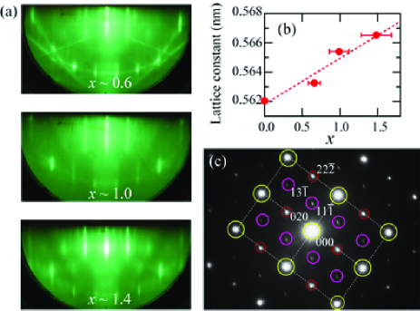
For the 100-nm-thick epilayers, we performed structural characterization by high-resolution x-ray diffraction with Cu radiation. As described in Ref. 11, since the (111) diffraction peak of the Fe3-xMnxSi layers could not be separated from the Ge(111) peak in -2 scans, we could not measure the out-of-plane lattice constant. To separate the diffraction peaks of the Ge substrate from those of the Fe3-xMnxSi layers, we measured reciprocal space maps for Fe3-xMnxSi(224), together with Ge (331). Assuming a cubic crystal structure, we can estimate the lattice constant for various from the (224) spacing . A plot of lattice constant (calculated from ) vs. is displayed in Fig. 1(b), together with that of an epitaxial Fe3Si ( 0) layer grown on Ge(111).Sadoh The figure shows that the lattice constant lengthens almost linearly with increasing . This tendency is in good agreement with that of bulk samples in previous works.Yoon ; Niculescu This result indicates that the doped Mn is systematically tuned. We also present cross-sectional selected-area diffraction (SAD) patterns of an Fe3-xMnxSi epilayer with 0.6 in Fig. 1(c). The SAD patterns clearly show super-lattice reflections due to the presence of the ordered structure, indicated by the pink solid circles. The two other diffraction patterns express the fundamental and super-lattice reflections, corresponding to the (yellow) and the ordered structures (red), respectively. Namely, the Fe3-xMnxSi epilayers include the ordered structure even for nonstoichiometric atomic compositions.
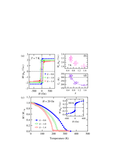
Using a superconducting quantum interference device (SQUID) magnetometer, we measured the magnetic properties of Fe3-xMnxSi epilayers for various . Figure 2 (a) shows the field-dependent magnetization (–) for 0.6, 1.0, and 1.4 at 7 K, where the vertical axis expresses the magnetic moment per formula unit. The magnetic field is applied parallel to the film plane with crystal orientation [01]. All the epilayers exhibit clear ferromagnetic hysteretic curves and the shape of the curves varies slightly for changes in . For 0.6, the coercivity is quite small compared to that of Fe2MnSi/Ge layers (i.e., 1)Ueda and is similar to that of Fe3Si/Ge layers.Sadoh ; Ionescu ; Ploog The saturation magnetization () at 7 K is summarized for various in Fig. 2(b). gradually changes with doping Mn composition.Yoon Figure 2(c) shows the temperature-dependent magnetization () for various in a small magnetic field of 20 Oe, where the magnetization is normalized by that at 7 K (/). For 1.0 (nearly stoichiometric composition), / disappears at 230 K, i.e., a Curie temperature () 230 K, largely consistent with that of bulk Fe2MnSi samples.Hongzhi ; Zhang For a nonstoichiometric composition of 0.6 or 1.4, becomes higher or lower than 230 K, respectively. It should be noted that for 0.6, finite magnetic moments are observed at 300 K. We also measured the – curve at 300 K, as shown in the inset of Fig. 2(c), and an evident ferromagnetic feature can be seen, i.e., room-temperature ferromagnetism. Figure 2(d) displays as a function of . also systematically changes with varying and room-temperature ferromagnetism is obtained at 0.6. These results demonstrate that our LT-MBE technique can realize control of ferromagnetism of Fe3-xMnxSi epilayers. We emphasize that the room-temperature ferromagnetic Fe3-xMnxSi epilayers include an -ordered structure, as described in Fig. 1(c).
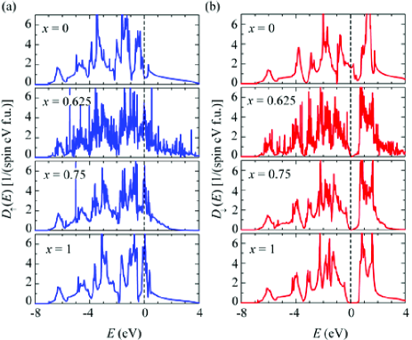
In order to discuss the electronic structure of the examined Fe3-xMnxSi with nonstoichiometric atomic compositions (), we carried out first-principles band calculations using the Vienna ab initio simulation package (VASP).Kresse The calculations are based on density functional theory (DFT) in the generalized gradient approximation (GGA). Although the electronic structure of Fe3-xMnxSi has been studied for Go using the TB-LMTO-ASA method,Andersen the electronic structure for has not yet been clarified. We hereafter consider that the crystal lattice structures of Fe3Si and Fe2MnSi are and types, respectively, and that the unit cell is composed of four interpenetrating fcc sub-lattices originating at A: , B: , C: , and D: . For both Fe3Si and Fe2MnSi, (A, C) sites and D sites are occupied by Fe atoms and Si atoms, respectively, and B sites are occupied by Fe atoms for Fe3Si and by Mn atoms for Fe2MnSi. For nonstoichiometric compositions, we consider super-cells consisting of eight atoms (), 16 atoms (, , , and ), 32 atoms ( and ), and 128 atoms (). For , we assume that Mn atoms enter B sites, as indicated by previous experiments.Yoon For , we assume that all B sites and some (A, C) sites are occupied by Mn atoms. Figures 3(a) and (b) show the densities of states (DOS), , calculated for spin-up () and spin-down () states, respectively. Here, we used a lattice constant optimized theoretically for -ordered Fe2MnSi. For the stoichiometric composition , the Fermi level () is situated within the band gap of the down-spin band, i.e., the electronic structure is half-metallic, which is consistent with previous predictions.Fujii ; Hongzhi We note that a half-metallic electronic structure can be seen even for a nonstoichiometric composition of . We define the spin polarization of the DOS as . Then, the half-metallic electronic structure () is obtained in the range . With decreasing , the half-metallicity tends to be lost and begins to decrease, but a high spin polarization of 0.9 remains down to 0.5. When is further reduced, decreases steeply and takes a negative value of for . It might be worth noting that the magnetic moment obtained for the half-metallic state () is well explained by the Slater-Pauling behavior of the full-Heusler alloys.Galanakis
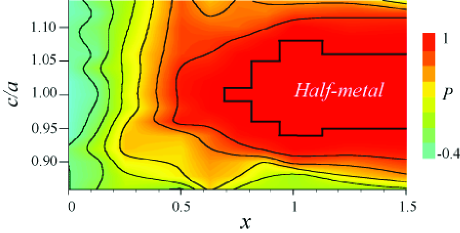
We also investigated theoretically how the electronic structure of Fe3-xMnxSi is affected by lattice distortion under biaxial compressive or tensile strain. Assuming (001) stacking and a constant volume of the unit cell, we introduce a tetragonal distortion, , where and are in-plane and out-of-plane lattice constants, respectively. Figure 4 shows a contour plot of obtained for various and . It is clear that gradually decreases with increasing lattice distortion. For the half-metallicity of 2Mn Heusler compounds, it is known that the energy level splitting between the and orbitals of the ions due to the crystal field in cubic symmetry is a crucial factor.Galanakis As the crystal lattice deviates from cubic (i.e., deviates from 1), the energy splitting shrinks and then the half-metallicity is lost, causing a decrease in . However, we find that the half-metallicity is stable in a relatively wide range of and for the Fe3-xMnxSi systems considered here. In experiments, although the bulk lattice constant of Fe3-xMnxSi () has been reported to be 0.5665 0.5672 nm,Yoon ; Niculescu ; Hongzhi ; Zhang that of our epilayer shown in Fig. 1(b) becomes 0.5654 nm, slightly smaller than the bulk value. It can be considered that the estimated lattice constant of the MBE-grown epilayer includes an effect due to lattice distortion. Hence, it is important for a full description of epitaxial Heusler compounds to understand the influence of lattice distortion on the half-metallicity. We note that the lattice distortion for 0.6 is quite small, 0.7%, where the converted is in the range 0.98 . Therefore, we can expect that room-temperature ferromagnetic Fe3-xMnxSi/Ge epilayers with 0.6 maintain a high spin polarization of 0.9, and this material can be used as spin injector and detector in Ge-based spintronic devices.
Because of interdiffusive solid-phase reactionsMaeda at the Fe3-xMnxSi/Ge interface, we could not utilize high-temperature processes ( 500 ∘C) to fabricate the magnetic tunnel junctions with Ge or MgO high-quality tunnel barriers. Thus, we cannot estimate the spin polarization of the Fe3-xMnxSi epilayers experimentally. To advance the next step for group-IV-semiconductor spintronics, we should further explore a method for the thermal stabilization of the Heusler compounds/Ge interfaces.
In summary, we have explored control of ferromagnetism and electronic structure of Heusler compounds Fe3-xMnxSi epitaxially grown on a group-IV semiconductor Ge. By tuning the Mn composition during LT-MBE growth, the saturation magnetization and Curie temperature can be controlled and we can fabricate -ordered structures, even for nonstoichiometric atomic compositions. We demonstrated that for a composition of 0.6, the Curie temperature exceeds 300 K. Theoretical calculations suggest that Fe3-xMnxSi alloys with nonstoichiometric compositions in the range 0.75 1.5 have a half-metallic electronic structure. The effect of lattice distortion on the spin polarization was also examined. It is expected that room-temperature ferromagnetic Fe3-xMnxSi/Ge epilayers maintain a high spin polarization of 0.9.
K.H. and M.M. wish to thank Y. Maeda, T. Sadoh, Y. Nozaki, Y. Terai, and Y. Ando for their helpful discussions, and S. Zaima, K. Matsuyama, M. Nishida, and Y. Kitamoto for providing the use of their facilities. This work was partly supported by a Grant-in-Aid for Scientific Research on Priority Area (No.18063018) from the Ministry of Education, Culture, Sports, Science, and Technology in Japan.
References
- (1) B. Min, K. Motohashi, C. Lodder, and R. Jansen, Nat. Mater. 5, 817 (2006); R. Jansen, Nat. Phys. 3, 521 (2007).
- (2) R. Nakane, M. Tanaka, and S. Sugahara, Appl. Phys. Lett. 89, 192503 (2006).
- (3) I. Appelbaum, B. Huang, and D. J. Monsma, Nature 447, 295 (2007).
- (4) B. T. Jonker, G. Kioseoglou, A. T. Hanbicki, C. H. Li, and P. E. Thompson, Nat. Phys. 3, 542 (2007).
- (5) O. M. J. van’t Erve, A. T. Hanbicki, M. Holub, C. H. Li, C. Awo-Affouda, P. E. Thompson, and B. T. Jonker, Appl. Phys. Lett. 91, 212109 (2007).
- (6) R. A. de Groot, F. M. Mueller, P. G. van Engen, and K. H. J. Buschow, Phys. Rev. Lett. 50, 2024 (1983).
- (7) Y. Lu, X. W. Li, G. Q. Gong, G. Xiao, A. Gupta, P. Lecoeur, J. Z. Sun, Y. Y. Wang and V. P. Dravid, Phys. Rev. B 54, R8357 (1996).
- (8) Y. Sakuraba, M. Hattori, M. Oogane, Y. Ando, H. Kato, A. Sakuma, T. Miyazaki, and H. Kubota, Appl. Phys. Lett. 88, 192508 (2006).
- (9) K. Inomata, N. Ikeda, N. Tezuka, R. Goto, S. Sugimoto, M. Wojcik, and E. Jedryka, Sci. Technol. Adv. Mater. 9, 014101 (2008).
- (10) T. Sadoh, M. Kumano, R. Kizuka, K. Ueda, A. Kenjo, and M. Miyao, Appl. Phys. Lett. 89, 182511 (2006); K. Ueda, Y. Ando, M. Kumano, T. Sadoh, Y. Maeda, and M. Miyao, Appl. Sur. Sci. 254, 6215 (2008).
- (11) K. Ueda, K. Hamaya, K. Yamamoto, Y. Ando, T. Sadoh, Y. Maeda, and M. Miyao, Appl. Phys. Lett. 93, 112108 (2008).
- (12) K. Hamaya, K. Ueda, Y. Kishi, Y. Ando, T. Sadoh, and M. Miyao, Appl. Phys. Lett. 93, 132117 (2008).
- (13) A. Ionescu, C. A. F. Vaz, T. Trypiniotis, C. M. Gürtler, H. García-Miquel, J. A. C. Bland, M. E. Vickers, R. M. Dalgliesh, S. Langridge, Y. Bugoslavsky, Y. Miyoshi, L. F. Cohen, and K. R. A. Ziebeck, Phys. Rev. B 71, 094401 (2005).
- (14) S. Fujii, S. Ishida, and S. Asano, J. Phys. Soc. Jpn. 64, 185 (1995).
- (15) L. Hongzhi, Z. Zhiyong ,M. Li, X. Shifeng, L. Heyan, Q. Jingping, L. Yangxian, and W. Guangheng, J. Phys. D: Appl. Phys. 40, 7121 (2007).
- (16) S. Yoon and J. G. Booth, J. Phys. F: Metal Phys. 7, 1079 (1977).
- (17) V. Niculescu, K. Raj, T. J. Burch, and J. I. Budnick, Phys. Rev. B 13, 3167 (1976).
- (18) J. Herfort, H. -P. Schönherr, and K. H. Ploog, Appl. Phys. Lett. 83, 3912 (2003); J. Herfort, H. -P. Schönherr, K.-J. Friedland, and K. H. Ploog, J. Vac. Sci. Technol. B 22, 2073 (2004).
- (19) L. Zhang, E. Bruck, O. Tegus, K. H. J. Buschow, and F. R. de Boer, Physica B 328, 295 (2003).
- (20) G. Kresse and J. Furthmüller, Phys. Rev. B 54, 11169 (1996).
- (21) A. Go, M. P.-Michalska, and L. Dobrzýnski, Eur. Phys. J. B 59, 1 (2007).
- (22) O. K. Andersen, Phys. Rev. B 12, 123060 (1975); O. K. Andersen and O. Jepsen, Phys. Rev. Lett. 53, 2571 (1984).
- (23) I. Galanakis, P. H. Dederichs, and N. Papanikolaou, Phys. Rev. B 66, 174429 (2002).
- (24) Y. Maeda, T. Jonishi, K. Narumi, Y. Ando, K. Ueda, M. Kumano, T. Sadoh, and M. Miyao, Appl. Phys. Lett. 91, 171910 (2007).