First-Principles Study for Evidence of Low Interface Defect Density at Ge/GeO2 Interfaces
Abstract
We present the evidence of the low defect density at Ge/GeO2 interfaces in terms of first-principles total energy calculations. The energy advantages of the atom emission from the Ge/GeO2 interface to release the stress due to the lattice mismatch are compared with those from the Si/SiO2 interface. The energy advantages of the Ge/GeO2 are found to be smaller than those of the Si/SiO2 because of the high flexibility of the bonding networks in GeO2. Thus, the suppression of the Ge-atom emission during the oxidation process leads to the improved electrical properties of the Ge/GeO2 interfaces.
pacs:
81.65.Mq, 68.35.-p, 71.15.Mb, 81.05.CyFor the past several decades, the performance of Si/SiO2 based transistor has been mainly accomplished by scaling the transistor dimensions resulting in a higher circuit speed, higher packing densities, and less power consumption. At present, the aggressive scaling of the SiO2 gate dielectric in silicon metal-oxide-semiconductor (MOS) devices leads to unacceptably high gate leakage currents. Thus, the scaling of advanced devices is approaching its technological and fundamental limits. To further improve the performance of complementary MOS devices, alternative channel materials are considered. Germanium is introduced as one of the promising candidates for beyond scaling devices, because the intrinsic carrier mobility of germanium is higher than that of silicon. To realize high-performance devices with germanium channel, one of the most crucial issues is the formation of gate stacks with superior interface properties. Ge/GeO2 interface is one of the most important issue because it exists even in Ge/high-k oxide interfaces. Although one might expect that germanium, as another elemental column-IV semiconductor, would behave similarly to silicon, the Ge/GeO2 interface had been generally considered to be more defective than the Si/SiO2 interface, in which the interface trap density typically lie in the range of the latter half of 1011 1012 cm-2eV-1 fukuda . Very recently, Matsubara et al. takagi have reported that the minimum value of the interface trap density lower than 1011 cm-2eV-1 can be obtained for Ge/GeO2 MOS interfaces fabricated by dry oxidation without any hydrogen passivation treatment. In addition, the current authors’ group (T. H. and H. W.) also accomplished high-quality Ge/GeO2 interfaces by conventional thermal treatment of germanium substrates hosoi .
On the theoretical side, the structural and electronic properties of the Ge/GeO2 interface have been investigated Pourtois ; houssa ; houssa2 . Houssa et al. houssa2 simulated the density of germanium dangling bonds at the Ge/GeO2 interface as a function of the oxidation temperature by combining viscoelastic data of GeO2 and the modified Maxwell’s model, and claimed that the density of germanium dangling bonds is less than that of silicon dangling bonds. Their results are in the good agreement with the experiments done by Matsubara et al. takagi and our result hosoi . The future development of the passivation technologies to deactivate the interface defects, by introducing terminators such as hydrogen, sulfur, silicon, and so on, will make it possible to achieve the lower interface defect density in Ge/GeO2. However, the formation of the defects in the Ge/GeO2 interface region during the oxidation process is not well-known.
In this Letter, we implement the first-principles total energy calculation of the Ge/GeO2 interface during the oxidation process. In the case of the Si/SiO2 interface, Kageshima and Shiraishi kageshima simulated oxidation processes by first principles. They found that a quartz structure can be obtained if silicon atoms are kicked out from the interface during oxidation, and these emitted silicon atoms might result in the creation of the interface defects. We compared the emission probabilities of the atom from the Ge/GeO2 and Si/SiO2 interfaces in terms of the total energy calculation following the oxidation process proposed by Kageshima and Shiraishi. To the best of our knowledge, this is the first theoretical investigation of the evidence of the low interface defect density at the Ge/GeO2 interfaces by first-principles total energy calculations. We found that the energy advantages of the germanium-atom emission are lower than that of the silicon-atom emission, and the small energy advantages are strongly related to the high flexibility of the bonding networks in GeO2.


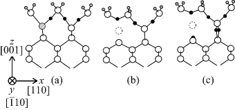
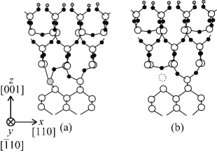
Our calculations were performed based on the density functional theory hk ; ks using the real-space finite-difference method che ; ho ; oh . In this method, basis sets used to expand wave functions are not required and boundary conditions are not constrained to be periodic. Our models are imposed the periodic boundary condition in the directions parallel to the surface and the isolated boundary condition in the direction perpendicular to the surface. The norm-conserving pseudopotentials of Troullier and Martins kb ; tm in the Kleinman-Bylander representation kobayashi were employed to describe the electron-ion interaction and the exchange-correlation potential was treated within the local density approximation pz . The cutoff energy was set at 112 Ry, which corresponds to a grid spacing of 0.30 a.u., and a further higher cutoff energy was set at 1011 Ry in the vicinity of the nuclei with the augmentation of the double-grid technique ho ; oh . Eight k-points in the 1 1 lateral unit cell were used for the Brillouin zone sampling. Figure 1 shows an example of the Ge(100) surface models. The initial structure of the surface model has nine germanium atomic layers, and the size of the supercell was and , where , , and are the lengths of the supercell in the , , and directions, respectively, and is the experimental lattice constant of the bulk comment . Both sides of the surface are simply terminated by hydrogen atoms. We sequentially inserted oxygen atoms between Ge-Ge bonds from the surface, assuming atomical layer-by-layer oxide growth, and finally introduced six oxygen atoms per unit cell. As the further oxidation model, Fig. 2 shows an example of the interface models. The initial structure of the interface model has three GeO2 molecule layers and seven germanium atomic layers. The length of the supercell in the direction was , and the other computational details were the same with those described in the surface models. We calculated the interface models inserted three or six oxygen atoms per unit cell into the interface region. During the first-principles structural optimization, we relaxed all the atoms except the germanium atoms in the bottom-most layer and the hydrogen atoms terminating their dangling bonds, reaching a tolerance in the force of 1.0 mH/bohr. For the comparison of the energy advantages between the cases of germanium and silicon, the same models for Si/SiO2 were also calculated.

| = 3 | = 6 | |
|---|---|---|
| Quartz/Ge(100) | 1.01 | 0.31 |
| Quartz/Si(100) | 0.13 | 3.94 |
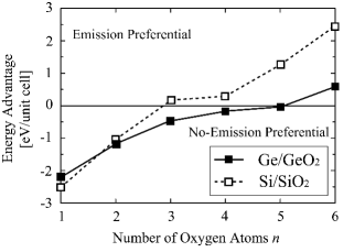
First, we examine the initial oxidation process of the substrates using the surface models. According to the oxidation process proposed by Kageshima and Shiraishi kageshima , the silicon atom in the second layer will be emitted to release the stress. Figures 1(a) and 1(b) show the examples for the case of , where is the number of the inserted oxygen atoms. The hatched silicon atom is kicked out and goes elsewhere. When is smaller than five, the dangling bonds remain at the interface after the emission. On the contrary, when six oxygen atoms are introduced, these dangling bonds are terminated by forming a Ge-O-Ge bond [see Fig. 1(c)]. Figure 3 shows the energy advantages of germanium and silicon as a function of the number of the inserted oxygen atoms. The energy advantage is defined as , where and are the total energies of the nonemitting and emitted structure with oxygen atoms inserted, respectively. In addition, is the chemical potential of the germanium or silicon in the bulk phase mucomment . The energy advantage of germanium for the atom emission is larger than that of silicon at because the formation energy of monovacancy is significantly smaller in germanium ( 1.9 eV) vacancy1 than silicon ( 3.3 eV) vacancy2 . On the other hand, the energy advantage of silicon increases more rapidly as the oxygen atoms are inserted and become larger than that of germanium. The silicon-atom emission from the surface model is preferential when is larger than three, while the germanium-atom emission is only at . We also examine the energy advantage of the atom emission from the interfaces as shown in Fig. 2. Table 1 summarizes the energy advantages for the emission from the interface, which are computed by the same manner with the case of the surface models. The energy advantage of germanium remains smaller than that of silicon. Although the quantitative discussion for the energy advantage is difficult because the chemical potentials of the atoms are simply computed from those in the bulk, our results indicate that the germanium atom preferentially stays in the substrate during the oxidation. In addition, if the germanium atoms are kicked out at , the two remaining dangling bonds are saturated by the reconstruction of the Ge-O-Ge bonding network as mentioned above. Since the event creating the dangling bonds at the interface scarcely happens, the defect density of the Ge/GeO2 interface becomes lower than that of the Si/SiO2 interface.
| Dispersion[degree2] | Thickness | |
|---|---|---|
| Ge | 283.4 | 0.43 |
| Si | 246.1 | 0.40 |
When oxygen atoms are sequentially inserted between Ge-Ge bonding networks from the surface, the formed oxide region has Ge-O-Ge bonding networks similar to that of the cristobalite of GeO2 bulk, and the bonding networks are attained lattice mismatch of 21 %, which is almost the same as the lattice mismatch between Si and SiO2. Therefore, the difference in the lattice mismatch is not strongly related to the small energy advantage of the Ge/GeO2 interface. Then, we compare the dispersions of the bonding angles in the GeO2 and SiO2 regions at which correspond to the 1-atomic-layer-oxidized surface. Table 2 shows the dispersions of the bonding angles from the tetrahedral structure of 109.5 degree and the thickness of the oxidized region. The larger dispersion of the bonding angles around germanium means that the bonding angles around germanium are more flexible than that around silicon. Therefore, the Young modulus of GeO2 is lower than that of SiO2 in the good agreement with the experiment young . Since the O-Si-O bonding angles keep the tetrahedral structure rigidly, the thickness of the SiO2 region barely increases to release the stress in the lattice mismatch while the GeO2 region elongates to the vacuum region. Thus, the high flexibility of the O-Ge-O bonding networks causes the small energy advantages of the germanium-atom emission, and then leads to the lower defect density at the Ge/GeO2 interface. Furthermore, the emitted atoms might cause the source of self-interstitials. The creation of these interstitials at the interface or in the substrate also becomes a serious problem because the interstitials cause the degradation of the MOS devices such as the dielectric leakage current and scattering centers of inversion carriers. Since the formation energy of the silicon self-interstitials ( 3.5 eV) is almost equal to that of germanium self-interstitials, the large energy advantage of silicon also gives rise to the self-interstitials at the interface gefe ; sife . Thus, our results imply that the Ge/GeO2 MOS field effect transistor exhibits the greater performance than the Si/SiO2 one owing to the lower interface trap density at its interface as well as high carrier mobility.
In conclusion, we have investigated the germanium- and silicon-atom emission during the oxidation process using the first-principles calculation. It is revealed that the germanium-atom emission hardly occurs compared with the silicon-atom emission because the high flexibility of the O-Ge-O bonding networks decreases the stress due to the lattice mismatch at the Ge/GeO2 interface. Our study supports the experimental results that the lower interface trap density will be realizable in the Ge/GeO2 interface. Since we studied only limited models of surfaces and interfaces, not all of the details of the actual process are included. Nevertheless, we believe that our study will help to design the germanium based device as the beyond scaling devices.
The authors would like to thank Professor Kikuji Hirose of Osaka University, Professor Kenji Shiraishi of University of Tsukuba, and Professor Hiroyuki Kageshima of NTT Basic Research Laboratories for reading the entire text in its original form and fruitful discussion. This research was partially supported by a Grant-in-Aid for the Global COE “Center of Excellence for Atomically Controlled Fabrication Technology”, by a Grant-in-Aid for Scientific Research in Priority Areas “Development of New Quantum Simulators and Quantum Design” (Grant No. 17064012), and also by a Grant-in-Aid for Young Scientists (B) (Grant No. 20710078) from the Ministry of Education, Culture, Sports, Science and Technology. The numerical calculation was carried out using the computer facilities of the Institute for Solid State Physics at the University of Tokyo, the Research Center for Computational Science at the National Institute of Natural Science, and the Information Synergy Center at Tohoku University.
References
- (1) H. Fukuda, T. Ueno, H. Kawarada, and I. Ohdomari, Jpn. J. Appl. Phys. 32, L569 (1993).
- (2) H. Matsubara, T. Sasada, M. Takenaka, and S. Takagi, Appl. Phys. Lett. 93, 032104 (2008).
- (3) Takuji Hosoi, Katsuhiro Kutsuki, Gaku Okamoto, Marina Saito, Takayoshi Shimura, and Heiji Watanabe submitted to Appl. Phys. Lett.
- (4) G. Pourtois, M. Houssa, A. Delabie, T. Conard, M. Caymax, M. Meuris, and M.M. Heyns, Appl. Phys. Lett. 92, 032105 (2008).
- (5) M. Houssa, G. Pourtois, M. Caymax, M. Meuris, and M.M. Heyns, Appl. Phys. Lett. 92, 242101 (2008).
- (6) M. Houssa, G. Pourtois, M. Caymax, M. Meuris, M.M. Heyns, V.V. Afanas’ev, and A. Stesmans, Appl. Phys. Lett. 93, 161909 (2008).
- (7) H. Kageshima and K. Shiraishi, Appl. Surf. Sci. 130-132, 176 (1998); Phys. Rev. Lett. 81, 5936 (1998).
- (8) P. Hohenberg and W. Kohn, Phys. Rev. 136, B864 (1964).
- (9) W. Kohn and L.J. Sham, Phys. Rev. 140, A1133 (1965).
- (10) J.R. Chelikowsky, N. Troullier, and Y. Saad, Phys. Rev. Lett. 72, 1240 (1994); J.R. Chelikowsky, N. Troullier, K. Wu, and Y. Saad, Phys. Rev. B 50, 11355 (1994).
- (11) K. Hirose, T. Ono, Y. Fujimoto, and S. Tsukamoto, First-Principles Calculations in Real-Space Formalism, Electronic Configurations and Transport Properties of Nanostructures (Imperial College, London, 2005).
- (12) T. Ono and K. Hirose, Phys. Rev. Lett. 82, 5016 (1999); Phys. Rev. B 72, 085115 (2005)
- (13) L. Kleinman and D.M. Bylander, Phys. Rev. Lett. 48, 1425 (1982).
- (14) N. Troullier and J.L. Martins, Phys. Rev. B 43, 1993 (1991).
- (15) We used the norm-conserving pseudopotentials NCPS97 constructed by K. Kobayashi; see K. Kobayashi, Comput. Mater. Sci. 14, 72 (1999).
- (16) J.P. Perdew and A. Zunger, Phys. Rev. B 23, 5048 (1981).
- (17) The experimental lattice constants are 10.67 a.u. for germanium and 10.26 a.u. for silicon.
- (18) The chemical potentials s are 3.97 and 3.96 a.u./atom for germanium and silicon, respectively.
- (19) A. Fazzio, A. Janotti, Antônio J.R. da Silva, and R. Mota, Phys. Rev. B 61, R2401 (2000).
- (20) M.J. Puska, S. Pöykkö, M. Pesola, and R.M. Nieminen, Phys. Rev. B 58, 1318 (1998).
- (21) E.M. Dianov and V.M. Mashinsky, J. Lightwave Technol. 23, 3500 (2005).
- (22) M.D. Moreira, R.H. Miwa, and P. Venezuela, Phys. Rev. B 70, 115215 (2004).
- (23) R.J. Needs, J. Phys.: Condens. Matter 11, 10437 (1999).