Inverse quantum spin Hall effect generated by spin pumping from precessing magnetization into a graphene-based two-dimensional topological insulator
Abstract
We propose a multiterminal nanostructure for electrical probing of the quantum spin Hall effect (QSHE) in two-dimensional (2D) topological insulators. The device consists of a ferromagnetic (FM) island with precessing magnetization that pumps (in the absence of any bias voltage) pure spin current symmetrically into the left and right adjacent 2D TIs modeled as graphene nanoribbons with the intrinsic spin-orbit (SO) coupling. In the reference frame rotating with magnetization, the device is mapped onto a DC circuit with twice as many terminals whose effectively half-metallic ferromagnetic electrodes are biased by the frequency of the microwave radiation driving the magnetization precession at the ferromagnetic resonance conditions. The QSH regime of the six-terminal TIFMTI nanodevice, attached to two longitudinal and four transverse normal metal electrodes, is characterized by the SO-coupling-induced energy gap, chiral spin-filtered edge states within finite length TI regions, and quantized spin Hall conductance when longitudinal bias voltage is applied, despite the presence of the FM island. The same unbiased device, but with precessing magnetization of the central FM island, blocks completely pumping of total spin and charge currents into the longitudinal electrodes while generating DC transverse charge Hall currents. Although these transverse charge currents are not quantized, their induction together with zero longitudinal charge current is a unique electrical response of TIs to pumped pure spin current that cannot be mimicked by SO-coupled but topologically trivial systems. In the corresponding two-terminal inhomogeneous TIFMTI nanostructures, we image spatial profiles of local spin and charge currents within TIs which illustrate transport confined to chiral spin-filtered edges states while revealing concomitantly the existence of interfacial spin and charge currents flowing around TIFM interfaces and penetrating into the bulk of TIs over some short distance.
pacs:
73.43.-f, 72.25.Pn, 76.50.+g, 72.80.VpI Introduction
The recent theoretical predictions Kane2005 ; Bernevig2006 ; Murakami2008 for the quantum spin Hall effect (QSHE) have attracted considerable attention by both basic and applied research communities. In the conventional SHE, Nagaosa2008 which manifests in multiterminal devices Nikoli'c2006 as pure spin current in the transverse electrodes driven by longitudinal unpolarized charge current in the presence of intrinsic (due to band structure) or extrinsic (due to impurities) spin-orbit (SO) couplings, the spin Hall conductance can acquire any value ( is the bias voltage applied between the longitudinal electrodes). Nagaosa2008 ; Nikoli'c2006 Conversely, becomes quantized in four-terminal devices that exhibit QSHE. Kane2005
The QSHE introduces an example of a new quantum state of matter—the so-called topological insulator (TI) Murakami2008 ; Kane2005a ; Xu2006a ; Qi2008 in two dimensions—which is a band insulator with a usual energy gap in the bulk, but which also accommodates gapless spin-polarized quantum states confined around the sample edges. Unlike closely related quantum Hall insulators, Jain2007 where the bulk energy gap and edge states appear due to an external magnetic field, TIs are time-reversal invariant systems whose intrinsic SO coupling opens a bulk gap while generating the Kramers doublet of edge states. These edge states force electrons of opposite spin to flow in opposite directions along the edges of the sample. Since time-reversal invariance ensures the crossing of the energy levels of such peculiar chiral and spin-filtered (or “helical” Bernevig2006 ; Murakami2008 ) edge states at special points in the Brillouin zone, the spectrum of a TI cannot be adiabatically deformed into topologically trivial insulator without such states. Kane2005a ; Xu2006a ; Qi2008
The recent experiments Konig2007 ; Konig2008 on HgTe quantum wells have confirmed some of the anticipated signatures Bernevig2006 of QSHE in line with transport taking place through helical edge states, such as: (i) reduction of the two-terminal charge conductance; (ii) its independence on the sample width; and (iii) sensitivity to an external magnetic field that destroys the TI phase. Nevertheless, this is still perceived as an indirect and incomplete detection because it did not confirm that conducting electrons along the edge were spin-polarized. The very recent nonlocal transport measurements on multiterminal HgTe microstructures in the QSH regime suggest that charge transport in these devices occurs through extended helical edge channels Roth2009 since their results can be explained via simple application of the Landauer-Büttiker scattering theory of multiprobe conductance to TIs attached to several metallic electrodes. Buttiker2009
Undoubtedly, the most convincing evidence for QSHE would be to measure quantized , as the counterpart of the quantized charge Hall conductance Jain2007 in the integer QHE exhibited by two-dimensional electron gases (2DEGs). However, this is quite difficult since pure spin currents Nagaosa2008 ; Nikoli'c2006 typically have to be converted into some electrical signal to be observed. Saitoh2006 ; Valenzuela2006 ; Seki2008 Thus, the key issue for unambiguous QSHE detection, as well as for the very definition of what constitutes direct experimental manifestation of 2D TIs, is to design Qi2008 devices where electrical quantities can be measured that are directly related to helical edge state transport and the corresponding quantization of .
The experiments Saitoh2006 ; Valenzuela2006 ; Seki2008 on the inverse SHE—where injection of pure spin current into a device with SO couplings leads to deflection of both spins in the same direction and corresponding Hall voltage between lateral sample boundaries or charge current in the transverse electrodes—provide guidance for QSHE probing via conventional electrical measurements. The devices constructed for these experiments are very flexible and allow for multifarious convincing tests confirming SHE physics. Seki2008 In particular, one of the inverse SHE experiments has injected pure spin current, generated by spin pumping Tserkovnyak2005 from a ferromagnetic (FM) layer with precessing magnetization driven by RF radiation at the ferromagnetic resonance (FMR) conditions, into a metal with SO couplings to observe the transverse Hall voltage. Saitoh2006
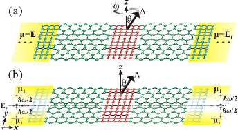
Here we propose a spin pumping-based nanostructure, illustrated in Fig. 1(a), where a FM island with precessing magnetization pumps, in the absence of any applied bias voltage, pure spin current into two adjacent graphene nanoribbons (GNR) with intrinsic SO coupling that act as the simplest model of 2D TI. Kane2005 ; Kane2005a This setup has an advantage Tserkovnyak2005 over other possible sources of pure spin currents because it evades the conductivity mismatch Nagaosa2008 between metallic injector and TI that would play a detrimental role when spin injection is driven by a bias voltage. Valenzuela2006 ; Seki2008 The three-layer central sample is attached to two metallic electrodes, and we also analyze six-terminal setups where additional four transverse electrodes, two per each GNR region, cover a portion of its top and bottom edge.
The nonequilibrium Green function (NEGF) picture of pumping, Chen2009 ; Hattori2007 which was utilized Chen2009 to explain very recent experiments Moriyama2008 on spin pumping across a band insulator within a magnetic tunnel junction, converts the complicated time-dependent problem posed by the device in Fig. 1(a) into a four-terminal DC circuit in Fig. 1(b) in the rotating reference frame. This picture also motivates the usage of a symmetric TIFMTI nanostructure since in asymmetric devices the central FM island would pump Chen2009 concomitantly a small charge current into the TI regions (with quadratic frequency dependence as opposed to dominant pumped spin current which is linear in frequency in the adiabatic limit). Within this framework we obtain the following principal results: (i) in the two-terminal device in Fig. 1(a), pumping generates both spin and charge local currents inside the TI, but only total spin current is non-zero (Figs. 3 and 4); (ii) imaging of local quantum transport in this two-terminal device also demonstrates the existence of interfacial spin and charge currents at the TIFM boundary, which are able to penetrate into the bulk of TIs over some short distance (Fig. 3); and (iii) in the corresponding six-terminal device whose TI regions are brought into the QSH regime, pumped total spin and charge currents vanish in the longitudinal leads, while non-zero charge currents emerge in the four transverse electrodes (p=3–6) as the manifestations of the inverse QSHE (Fig. 6). The charge conductances , however, are not quantized.
It is worth recalling that 2D TIs, also denoted as QSH insulators, were initially studied as isolated infinite homogeneous systems. Murakami2008 On the other hand, experiments require to embed such materials into circuits where they will be attached to multiple metallic electrodes serving as current or voltage probes. Roth2009 For example, the very recent analysis has predicted highly unusual spin dynamics at the TInormal-metal Yokoyama2009 and TIFM Maciejko2009 interfaces. This, together with our findings of interfacial currents around TIFM junction highlights the need to understand operation of inhomogeneous nanostructures, with multiple TImetal interfaces and helical edge states of finite extent, Roth2009 as a prerequisite for the design of anticipated spintronic devices Maciejko2009 exploiting TIs. Similar issues, albeit without spin dynamics, were encountered in the well-known experiments Haug1989 on inhomogeneous (e.g., containing a potential barrier) multiterminal quantum Hall bridges where a simple picture of edge transport becomes insufficient and one has to take into account trajectory network Haug1989 ; Gagel1996 connecting edge channels across the bulk of the device. Jain2007
The paper is organized as follows. In Sec. II, we discuss the effective Hamiltonian of the device and NEGF approach to computation of pumped spin and charge currents in the picture of the rotating reference frame. The images of local pumped spin and charge currents are shown in Sec. III for unbiased two-terminal device, while total quantized spin Hall currents in biased and pumped charge currents in the transverse electrodes of unbiased six-terminal devices are studied in Sec. IV. Section V is devoted to explaining the origin of non-quantized transverse charge currents and zero total spin and charge current in the longitudinal electrodes of our inverse QSHE device using the picture of possible Feynman paths Buttiker2009 of spin-polarized injected and collected electrons within the 12-terminal DC device in the rotating frame. We also support the conjectured network of such paths using spatial profiles of local currents computed for the 12-terminal DC device. We conclude in Sec. VI.
II NEGF approach to spin pumping in multiterminal QSH systems
The central TIFMTI region of the nanostructure in Fig. 1 can be described by the effective single -orbital tight-binding Hamiltonian in the laboratory frame:
| (1) | |||||
Here is the vector of spin-dependent electron creation operators and is the vector of the Pauli matrices. For simplicity, the usual (spin-independent) nearest-neighbor hopping is assumed to be the same for the square lattice of FM island and the semi-infinite leads, as well as for the hopping that couples different regions of the device. On the honeycomb lattice of TI regions, eV can reproduce Areshkin2009a ab initio computed band structure very close to the charge neutral Dirac point ().
The coupling of itinerant electrons to collective magnetic dynamics is described through the material-dependent exchange potential , which is non-zero only in the FM island. The on-site potential can accommodate disorder, Sheng2005b ; Qiao2008 external electric field, or band bottom alignment. The Hamiltonian (1) is time-dependent since the spatially uniform unit vector along the local magnetization direction is precessing steadily around the -axis with a constant cone angle and frequency . The central TIFMTI region is attached to two or six semi-infinite ideal (spin and charge interaction free) electrodes, modeled on the same square lattice as the FM island, which terminate in macroscopic reservoirs held at the same electrochemical potential .
The third sum in Eq. (1) is non-zero only in the GNR regions where it introduces the intrinsic SO coupling compatible with the symmetries of the honeycomb lattice. The SO coupling, which is responsible for the band gap Kane2005 , acts as spin-dependent next-nearest neighbor hopping where and are two next-nearest neighbor sites, is the only common nearest neighbor of and , and is a vector pointing from to .
Among several proposals for QSHE, Murakami2008 ; Konig2008 graphene with stands out as the simplest model employed to introduce QSHE phenomenology, Kane2005 classification of TIs, Kane2005a and manifestations of QSHE in realistic multiterminal devices, Sheng2005b ; Qiao2008 as well as to analyze disorder Xu2006a ; Sheng2005b ; Qiao2008 and interaction Xu2006a ; Zarea2008 effects on TIs. However, recent scrutiny finding minuscule V through density functional theory (DFT) calculations Min2006 would push the requirement for the observation of QSHE in graphene toward unrealistically low temperatures Konig2008 K. However, these calculations are not fully first-principles and all-electron—a direct all-electron (i.e., no pseudopotential) DFT approach Boettger2007 ; Gmitra2009 has estimated K, which makes the device in Fig. 1 experimentally realizable. The physical explanation of an apparent controversy between extremely small intrinsic SO coupling found in Refs. Min2006, and non-negligible values computed in Refs. Boettger2007, ; Gmitra2009, is in the fact that 96% of the intrinsic SO splitting in graphene originates from the usually neglected and higher orbitals. Gmitra2009
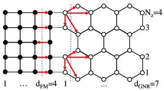
We select the following device parameters in the analysis and Figures below: , , , GHz and . The geometry and size of zigzag GNR (ZGNR) and FM regions of the device shown in Fig. 1 is characterized by: -ZGNR is composed of zigzag chains so that its average width is ( Å is the lattice spacing of the honeycomb lattice); is the number of atoms along the zigzag chain defining its length ; and is the thickness of the FM island. For illustration of , , and parameters see Fig. 2.
Note that the selected value Kane2005 for is much larger than the one that would be fitted to first-principles calculations. Boettger2007 ; Gmitra2009 The reason for this choice (in fact, even larger values have been employed in recent studies Sheng2005b ; Qiao2008 ; Zarea2008 ) is the usage of the effective tight-binding Hamiltonian (1) which in the case of vastly different energy scales would make quantum transport calculations insensitive to the presence of . On the other hand, this does not affect any conclusions about quantized spin transport properties of a graphene-based model of a TI since they do not depend on the particular value of and simply require to perform measurements at temperatures where the band gap of the TI is visible while its Fermi energy is within such gap.
Although widely-used scattering theory Tserkovnyak2005 of adiabatic spin pumping by FMnormal-metal (FMNM) interfaces, typically combined with the spin-diffusion equation and magnetoelectric circuit theory, cannot handle nanostructures containing insulators of band (due to spin accumulation not being well-defined in them) or topological type (due to necessity to take into account details of one-dimensional transport through helical edge states), the NEGF approach to spin pumping Chen2009 ; Hattori2007 can describe both cases by taking the microscopic Hamiltonian (1) as an input. The unitary transformation of Eq. (1) via [for precessing counterclockwise] leads to a time-independent Hamiltonian in the rotating frame: Chen2009 ; Hattori2007
| (2) |
The Zeeman term , which emerges uniformly in the sample and the NM electrodes, will spin-split the bands of the NM electrodes, thereby providing a rotating frame picture of pumping based on the four-terminal DC device in Fig. 1(b). This term breaks time-reversal invariance (while conserving spin ), but for typical FMR frequencies Moriyama2008 of the order of 1 GHz, it is smaller than Boettger2007 ; Gmitra2009 V.
The basic transport quantity for the DC circuit in Fig. 1(b) is the spin-resolved bond charge current Nikoli'c2006 ; Onoda2005a carrying spin- electrons from site to site
| (3) |
This is obtained in terms of the lesser Green function Haug2007 in the rotating frame Chen2009 ; Hattori2007 . Unlike in the laboratory frame, depends on only one time variable (or energy after the time difference is Fourier transformed Nikoli'c2006 ). This yields spin
| (4) |
and charge
| (5) |
bond currents flowing between nearest neighbor or next-nearest neighbor sites and if they are connected by hopping . The definition of bond currents is illustrated in Fig. 2, both for the square lattice of FM and the honeycomb lattice of the chosen 2D TI model.
The rotating frame four-terminal device in Fig. 1(b), or its twelve-terminal counterpart originating from a six-terminal QSH bridge [illustrated by insets in Fig. 6], guides us in constructing the NEGF equations for the description of currents flowing between their electrodes. The electrodes in the rotating frame are labeled by () [ and ] and they are biased by the electrochemical potential difference . Thus, these electrodes behave as effective half-metallic ferromagnets which emit or absorb only one spin species.
The rotating frame retarded Green function Chen2009 ; Hattori2007
| (6) |
and the lesser Green function
| (7) |
describe the density of available quantum states and how electrons occupy those states, respectively. Here is the matrix representation of (2) in the basis of local orbitals. The retarded self-energy matrix is the sum of retarded self-energies introduced by the interaction with the leads which determine escape rates of spin- electron into the electrodes .
For noninteracting systems described by the Hamiltonian (2), the lesser self-energy is expressed in terms of as
| (8) |
The level broadening matrix in the rotating frame
| (9) |
is obtained from the usual self-energy matrices Haug2007 of semi-infinite leads in the laboratory frame with their energy argument being shifted by to take into account the “bias voltage” in accord with Fig. 1(b). The distribution function of electrons in the electrodes of the rotating frame DC circuit is given by
| (10) |
where for spin- and for spin-.
III Local and total currents in two-terminal TIFMTI devices
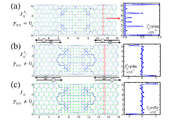
The spatial imaging of local spin currents has played an important role in understanding how QSHE Onoda2005a or mesoscopic SHE Nikoli'c2006 due to intrinsic SO couplings manifest in experimentally accessible multiterminal devices. In Fig. 3(a), we first establish a reference local-current-picture of pumping for ZGNRFMZGNR device with no SO coupling in ZGNR regions. Its transport properties are governed Zarbo2007 by the edge-localized quantum states induced by the topology of the chosen zigzag edges. Murakami2008 ; Zarea2008 The non-zero SO coupling in Eq. (1) converts the ZGNR regions into a 2D TI by opening energy gap and by forcing their strongly-localized states Murakami2008 ; Zarbo2007 to become spin-filtered and to acquire a linear dispersion around crossing the band gap Kane2005 ; Zarea2008 (SO coupling additionally suppresses their unscreened Coulomb interaction Zarea2008 ).
Using the picture of such helical edge states within the TI regions of
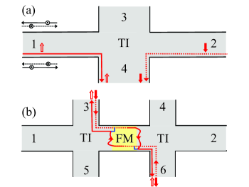
the DC device in Fig. 1(b), whose spin and chirality is illustrated in Fig. 3(b), we can follow possible Feynman paths of electrons in Fig. 3. For example, a spin- electron from (,) electrode at a higher electrochemical potential can only flow along the top left edge then it precesses through the FM island (because it is not an eigenstate of term in ) enters with some probability into spin- edge state on the bottom right edge finally, it is collected by (,) electrode at a lower electrochemical potential . The spin- electron injected by (,) lead would retrace the same path in the opposite direction on the way toward (,) electrode.
According to these straightforward paths, one expects no chiral edge currents around bottom left and top right edges of the device. However, these currents do exist in Figs. 3(b) and 3(c) due to more subtle backscattering effects at the TIFM interface. They are the consequence of the paths, clearly visible in Fig. 3, where, e.g., spin- electron from (,) electrode is reflected and rotated Maciejko2009 at the TIFM interface (where FM region breaks the time-reversal invariance) to flow backward through spin- edge state then it propagates along the left-NM-leadTI interface it flows along the bottom left edge, FM island, and bottom right edge to finally enter into (,) electrode at electrochemical potential . This process can also account for the difference between spin currents flowing along the top and bottom edges of a single TI region, which yields non-zero total spin current in Fig. 4.
Another set of transverse current paths, conspicuously visible in Figs. 3(b) and 3(c), emerges around TIFM interfaces. These interfacial spin and charge currents are able to penetrate slightly into the bulk of the TIs, Onoda2005a in contrast to infinite homogeneous (i.e., all TI) systems where current flow is strictly confined to sample edges. Murakami2008
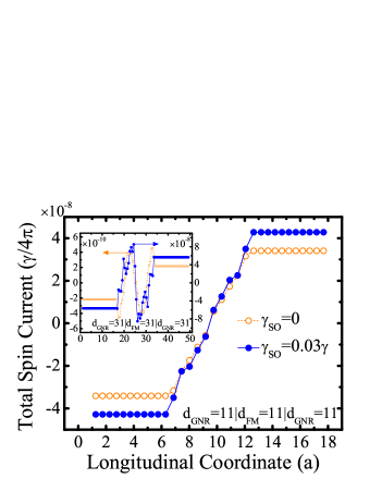
Figure 4 plots the total spin current along the device, which is obtained by summing local nearest-neighbor and next-nearest-neighbor bond currents at each transverse cross section in Fig. 3. Although non-zero locally, the total charge current through any cross section in Fig. 3(c), including the left and right electrodes, remains zero. Since typical spin-relaxation lengths are much longer than the length scale over which pumping develops, Tserkovnyak2005 we assume that FM island is clean so that non-conserved spin currents emerge throughout its volume. The magnitude of spin current pumped into GNRs is set around the GNRFM interface, Chen2009 and it is enhanced by the presence of helical edge states (for ), contrary to naïve expectation that FMTI interface would be less transparent for spin injection.
IV Local and total currents in six-terminal TIFMTI devices
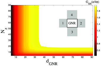
To obtain sharp conductance steps in quantum transport calculations of the integer QHE in realistic (e.g., consisting of carbon atoms Kazymyrenko2008 ) six-terminal mesoscopic all-graphene Hall bars requires to avoid reflection at the leadsample interface by using magnetic field both in the sample and in the semi-infinite leads, as well as by employing high quality contacts. Kazymyrenko2008 Thus, it is somewhat surprising that perfectly quantized was obtained in Ref. Sheng2005b, for a four-terminal graphene-based 2D TI device where SO coupling is present only in the sample and whose metallic electrodes, for a chosen square lattice model, have propagating modes that couple poorly to evanescent and propagating modes within GNRs. Robinson2007 In fact, the corresponding contacts metallic-electrodezigzag-GNR in those devices act as effective disorder by introducing mixing of transverse propagating modes defined by the semi-infinite ideal leads. Areshkin2009a
Figure 5 extends findings of Ref. Sheng2005b, , obtained for special graphene ribbon aspect ratios (, , ) and leads attached to a segment of the ribbon edge, to confirm that can be obtained in any sufficiently Zhou2008 wide and long graphene ribbon attached to four metallic electrodes. Here the square lattice leads cover the whole top or bottom lateral graphene edge, while the longitudinal leads are attached at armchair edges as shown in Fig. 2. The square lattice of the leads is selected to be “lattice-matched” (lattice constant is the same as carbon-carbon distance in GNR as illustrated by Figs. 1 and 2) in order to reduce the detrimental effects of the contacts (i.e., the transmission matrix of the two-terminal device NMGNRNM has smaller off-diagonal elements than when “lattice-unmatched” square lattice leads are employed to model metallic electrodes). Areshkin2009a
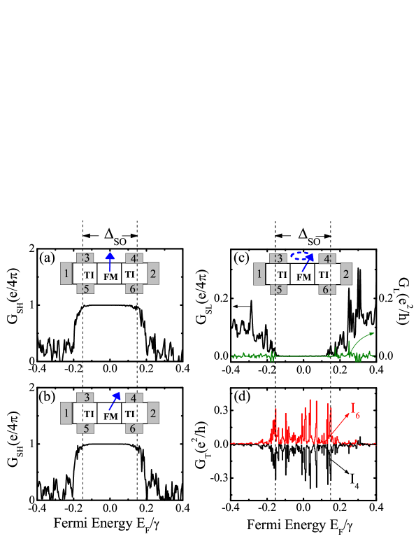
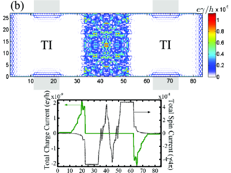
In order to generate non-zero total charge current response of the 2D TIs, we attach additional four electrodes (Fig. 6) at the top and bottom edges of the device in Fig. 1(a) of length and width . The two longitudinal electrodes and additional four transverse electrodes (covering 10 edge carbon atoms) are modeled on the same “lattice-matched” square lattice. Such six-terminal bridge, when biased by the voltage difference , exhibits quantized shown in Fig. 6(a), despite the fact that it is not identical to standard homogeneous QSH bridges Roth2009 since it contains FM island in the middle breaking the continuity of helical edge states. Furthermore, we confirm that quantization of is independent of the angle by which static FM magnetization is tilted from the -axis, as illustrated by Fig. 6(b).
Since , we can use at low temperatures for the difference of the Fermi functions present Chen2009 in Eq. (3). This “adiabatic approximation” Hattori2007 is analogous to linear response calculations for biased devices, allowing us to define the longitudinal spin conductance and transverse charge conductance for the device whose FM magnetization is precessing with frequency . In the unbiased () six-terminal TIFMTI device, Fig. 6(c) shows that vanishes when is within the SO gap, while non-zero charge Hall currents emerge in transverse electrodes so that in Fig. 6(d). Moreover, transverse charge currents obtained in the regime of the QSH insulator (marked by gap in Fig. 6) are the signature of the inverse QSHE since only in this range of Fermi energies we get and characterizing the usual charge Hall effect. However, we find that is not quantized. Note that the same conclusions are reached when the electrodes are made of the same TI as in the central region of the QSH bridge.
Figure 6(c) also shows that total charge current pumped into the longitudinal leads is zero within the QSH insulator regime (), which is quite different from the conventional inverse SHE driven by spin pumping from precessing magnetization into a topologically trivial SO-coupled systems, such as the multiterminal 2DEG with the Rashba SO coupling. Ohe2008 In the latter case, AC charge currents (with small DC contribution vanishing as the 2DEG size increase) are pumped into both transverse and longitudinal electrodes. Their time-dependence originates from spin non-conservation in the presence of the Rashba SO coupling, unlike in our case where charge and spin- currents are time-independent in both rotating and laboratory frames since spin is conserved.
V Discussion
The presence of extended chiral edge states in QH and QSH systems makes the analysis of transport measurements based on the Landuaer-Büttiker multiprobe formulas Buttiker2009 particularly simple assuming homogeneous bridge, such as the TI central region attached to electrodes made of the same TI material Kane2005 ; Buttiker2009 or 2DEG and graphene in high magnetic field attached to the same type of electrodes in the same magnetic field. Kazymyrenko2008 In those cases, the extended edge states are perfectly matched across the whole device and one can simply draw Kane2005 ; Buttiker2009 a picture of allowed trajectories (or “Feynman paths”), for whom the quantum edge states serve as guiding centers, to count their contribution (as ballistic one-dimensional conductors) to current in a selected electrode.
Following Ref. Kane2005, , we show such paths for the inverse QSHE in Fig. 7(a) based on an abstract scheme where pure spin current is injected through the longitudinal leads due to different electrochemical potentials for spin- and spin- states, and driving two counter-propagating fully spin-polarized longitudinal charge currents. In this case, continuity of the edge states and absence of any reflection between the leads and the sample ensures that conductance associated with transverse charge current is quantized. Kane2005 However, the setup is unrealistic from the experimental viewpoint because it requires separate control of electrochemical potentials for spin- and spin- carriers within the same electrode.
On the other hand, the presence of FM region in our devices breaks the continuity of edge states, thereby making the network of Feynman paths much more complicated. The analogous issues have been explored in experiments Haug1989 on QH bridges where the gate electrode covering small portion of the central region introduces backscattering between spatially separated edge states, thereby requiring complicated trajectory network Haug1989 or spatial profiles of local currents Gagel1996 to explain non-quantized features in the longitudinal resistance. Furthermore, in the case of our six-terminal TIFMTI bridge, the breaking of time-reversal invariance at the TIFM interface by the nearby FM island also enables spin-dependent reflection where incoming electron from a helical edge state has its spin rotated to be injected in the counter-propagating helical edge state along the same edge of the sample. Maciejko2009
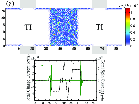
Nevertheless, some of the important paths can be extracted from spatial profiles of local currents in Fig. 3 for the two-terminal TIFMTI device or Fig. 8 for the six-terminal TIFMTI device. This allows us to explain all of the key results on the inverse QSHE driven by spin pumping shown in Fig. 6 for total terminal currents. The possible electron paths are easier to draw for the six-terminal TIFMTI device whose electrodes are made of the same TI, and can be understood using the picture of twelve effectively half-metallic FM electrodes in the rotating frame which try to inject their fully spin-polarized electrons into chiral spin-filtered edge states moving in proper direction.
For example, Fig. 7(b) shows spin- electrons starting from lead (3, ) at a higher electrochemical potential to enter the right moving spin- helical state on the top edge. The electrons have probability to penetrate into the FM island where they precess and continue to propagate down (e.g., through interfacial spin currents shown in Fig. 3 and Fig. 8 along the right FMTI interface) to finally enter the bottom helical edge state as spin- particles which allows them to be collected by the electrode (6, ) at lower electrochemical potential . At the same time, incoming electrons from lead (3, ) can also be reflected at the TIFM interface where accompanying spin rotation Maciejko2009 makes it possible for them to propagate back into the lead (3,) which they enter as spin- electron with some probability. Portions of this path are retraced by spin- electron from lead (6,) flowing toward lead (3,), where reflection and spin rotation at the right TIFM interface generate additional current of spin- electrons into lead 6 to produce total charge current whose sign is compatible with the exact calculations shown in Fig. 6(d). These paths also explain the absence of quantization of conductance in Fig. 6(d) since transport which generates non-zero longitudinal charge currents is not confined solely to the helical edge states as in Fig. 7(a).
While the selected paths in Fig. 7 are compatible with complete (numerically exact) spatial profiles of local charge currents shown in Fig. 8(a), the profiles also contain trivial strictly edge paths carrying non-zero local charge and spin currents between leads 4 and 2 due to ballistic transport of spin- electrons from electrode toward with higher state occupancy then for spin- electrons propagating from toward electrode. Since the same local currents exists along the opposite edge connecting electrodes 6 and 2, the total spin or charge current flowing into the longitudinal electrode 2 is identically equal to zero [see inset below Fig. 8(a)]. The same conclusion holds by symmetry for leads 1, 3, and 5 on the opposite side of bridge. Thus, the absence of any Feynman paths that would allow electrons from (1,) and (2,) electrodes to reach some other (,) electrode via propagation through helical edge states, combined with trajectories within FM or along the TIFM interface, confirms one of the key results in Fig. 6(c)—absence of longitudinal spin and charge currents in the spin-pumping-induced inverse QSHE.
We also note that the above discussion becomes more complicated for the TIFMTI bridges with six NM electrodes that were actually employed in Fig. 6. This is exemplified by Fig. 8(b) where new paths have to be take into account that allow electrons to propagate along interfaces between TI regions and the attached NM electrodes while also penetrating Onoda2005a into the bulk of NM electrodes where there are no helical edge states. In the case of leads 1 and 2, local currents around TINM interface penetrate only slightly into the bulk of the NM electrodes and then return toward TI to ensure zero total spin and charge currents in the longitudinal electrodes, as demonstrated by the inset below Fig. 8(b).
VI Concluding Remarks
Using the mapping of time-dependent spin pumping by precessing magnetization to a multiterminal DC device in the rotating frame, we describe injection of thus generated local and total spin currents into helical edge states of a topological insulator in the absence of any externally applied bias voltage. In the regime where the voltage biased six-terminal TIFMTI nanodevice exhibits QSHE, the corresponding unbiased device with precessing FM magnetization generates charge currents in the transverse electrodes (characterized by and ), while bringing pumped total spin and charge currents in longitudinal electrodes to zero. Although the transverse charge conductance of such inverse QSHE is not quantized, these two responses to pumping can be used to probe the TI phase via unambiguous electrical measurements. The absence of quantization of transverse charge conductances was explained as the consequence of electron propagation paths being composed of both simple segments guided by chiral spin-filtered edge states of finite extent and more complicated segments through the FM island or around the TIFM interface where spin-dependent reflection accompanied by spin rotation can take place. Our analysis based on imaging of local (i.e., on the scale of the lattice constant) spin and charge transport reveals interfacial currents around TIFM interfaces that can penetrate slightly into the bulk of the TI or interfacial currents around TINM-electrode contacts which break the continuity of helical edge states.
Although a topologically trivial system with the intrinsic SO couplings (such as the Rashba spin-split 2DEG Nikoli'c2006 ) would also generate non-quantized transverse charge currents in response to pure spin currents pumped by precessing magnetization, Ohe2008 this setup also pumps longitudinal charge currents. Ohe2008 This is completely different from the behavior of the proposed TIFMTI multiterminal device. In addition, for SO couplings which do not conserve spin (such as the Rashba one), both transverse and longitudinal pumped charge currents are time-dependent, Ohe2008 as opposed to DC transverse charge Hall currents generated by our device.
During the preparation of this manuscript we became aware of the theoretical proposal Qi2008 for a charge pumping device designed to induce electrical response of a 2D TI where two FM islands, one with precessing and one with fixed magnetization, are deposited on the top and bottom edges, respectively, of a QSH insulator attached to two electrodes. While the physical motivation leading to this device—fractional charge response to magnetic domain wall acting as external physical field—is different from ours, its operation can be easily explained from our four-terminal DC device picture (Fig. 1) of spin and charge pumping in the rotating frame. That is, the top FM island (see Fig. 3 in Ref. Qi2008, ) injects pure spin current into upper helical edge states of the QSH insulator, which is then partially converted into charge current flowing along the edges as explained by spatial profiles of local charge currents in Fig. 3(c). The role of the bottom FM island in this setup is to block the local charge current, which otherwise flows in the opposite direction along the bottom edge in Fig. 3(c) leading to in our device setup. Such blocking is based on a simple observation that FM region whose magnetization is collinear with the magnetization of the effective half-metallic electrodes in the rotating frame does not permit any transport through it that connects these electrodes. However, it is unclear if such two-terminal device can display perfectly quantized longitudinal charge current (or, equivalently, quantized conductance in our notation) in a realistic setup, which was conjectured in Ref. Qi2008, via qualitative arguments without treating the effect of TIFM interfaces on adiabatic charge pumping through either the scattering Tserkovnyak2005 or NEGF Chen2009 ; Hattori2007 approaches.
Acknowledgements.
This work was supported by DOE Grant No. DE-FG02-07ER46374 through the Center for Spintronics and Biodetection at the University of Delaware. C.-R. Chang was supported by the Republic of China National Science Council Grant No. 95-2112-M-002-044-MY3.References
- (1) C. L. Kane and E. J. Mele, Phys. Rev. Lett. 95, 226801 (2005).
- (2) B. A. Bernevig, T. L. Hughes, and S.-C. Zhang, Science 314, 1757 (2006).
- (3) S. Murakami, Prog. Theor. Phys. Suppl. 176, 279 (2008).
- (4) N. Nagaosa, J. Phys. Soc. Jpn. 77, 031010 (2008).
- (5) B. K. Nikolić, L. P. Zârbo, and S. Souma, Phys. Rev. B 73, 075303 (2006).
- (6) C. L. Kane and E. J. Mele, Phys. Rev. Lett. 95, 146802 (2005).
- (7) C. Xu and J. E. Moore, Phys. Rev. B 73, 045322 (2006).
- (8) X.-L. Qi, T. L. Hughes, and S.-C. Zhang, Nature Phys. 4, 273 (2008).
- (9) J. K. Jain, Composite Fermions (Cambridge University Press, Cambridge, 2007).
- (10) M. König, S. Wiedmann, C. Brüne, A. Roth, H. Buhmann, L. W. Molenkamp, X.-L. Qi, and S.-C. Zhang, Science 318, 766 (2007).
- (11) M. König, H. Buhmann, L. W. Molenkamp, T. Hughes, C.-X. Liu, X.-L. Qi and S.-C. Zhang, J. Phys. Soc. Jpn. 77, 031007 (2008).
- (12) A. Roth, C. Brüne, H Buhmann, L. W. Molenkamp, J. Maciejko, X.-L. Qi, and S.-C. Zhang, Science 325, 294 (2009).
- (13) M. Büttiker, Science 325, 278 (2009); M. Büttiker, Phys. Rev. B 38, 9375 (1988).
- (14) E. Saitoh, M. Ueda, H. Miyajima, and G. Tatara, Appl. Phys. Lett. 88, 182509 (2006); K. Ando, Y. Kajiwara, S. Takahashi, S. Maekawa, K. Takemoto, M. Takatsu, and E. Saitoh, Phys. Rev. B 78, 014413 (2008).
- (15) S. O. Valenzuela and M. Tinkham, Nature 442, 176 (2006).
- (16) T. Seki, Y. Hasegawa, S. Mitani, S. Takahashi, H. Imamura, S. Maekawa, J. Nitta, and K. Takanashi, Nature Mater. 7, 125 (2008).
- (17) Y. Tserkovnyak, A. Brataas, G. E. W. Bauer, and B. I. Halperin, Rev. Mod. Phys. 77, 1375 (2005).
- (18) S.-H. Chen, C.-R. Chang, J. Q. Xiao, and B. K. Nikolić, Phys. Rev. B 79, 054424 (2009).
- (19) K. Hattori, Phys. Rev. B 75, 205302 (2007); J. Phys. Soc. Jpn. 77, 034707 (2008).
- (20) T. Moriyama, R. Cao, X. Fan, G. Xuan, B. K. Nikolić, Y. Tserkovnyak, J. Kolodzey, and J. Q. Xiao, Phys. Rev. Lett. 100, 067602 (2008).
- (21) T. Yokoyama, Y. Tanaka, and N. Nagaosa, Phys. Rev. Lett. 102, 166801 (2009).
- (22) J. Maciejko, E.-A. Kim, and X.-L. Qi, preprint arXiv:0908.0564.
- (23) R. J. Haug, J. Kucera, P. Streda, and K. von Klitzing, Phys. Rev. B 39, 10892 (1989).
- (24) F. Gagel and K. Maschke, Phys. Rev. B 54, 10346 (1996).
- (25) D. A. Areshkin and B. K. Nikolić, Phys. Rev. B 79, 205430 (2009).
- (26) L. Sheng, D. N. Sheng, C. S. Ting, and F. D. M. Haldane, Phys. Rev. Lett. 95, 136602 (2005).
- (27) Z. Qiao, J. Wang, Y. Wei, and H. Guo, Phys. Rev. Lett. 101, 016804 (2008).
- (28) M. Zarea, C. Büsser, and N. Sandler, Phys. Rev. Lett. 101, 196804 (2008).
- (29) H. Min, J. E. Hill, N. A. Sinitsyn, B. R. Sahu, L. Kleinman, and A. H. MacDonald, Phys. Rev. B 74, 165310 (2006); Y. Yao, F. Ye, X.-L. Qi, S.-C. Zhang, and Z. Fang, Phys. Rev. B 75, 041401(R) (2007).
- (30) J. C. Boettger and S. B. Trickey, Phys. Rev. B 75, 121402(R) (2007).
- (31) M. Gmitra, S. Konschuh, C. Ertler, C. Ambrosch-Draxl, and J. Fabian, preprint arXiv:0904.3315 (to appear in Phys. Rev. B).
- (32) H. Haug and A.-P. Jauho, Quantum Kinetics in Transport and Optics of Semiconductors 2nd Ed. (Springer, Berlin, 2007).
- (33) M. Onoda and N. Nagaosa, Phys. Rev. Lett. 95, 106601 (2005).
- (34) L. P. Zârbo and B. K. Nikolić, EPL 80, 47001 (2007).
- (35) K. Kazymyrenko and X. Waintal, Phys. Rev. B 77, 115119 (2008).
- (36) J. P. Robinson and H. Schomerus, Phys. Rev. B 76, 115430 (2007).
- (37) B. Zhou, H.-Z. Lu, R.-L. Chu, S.-Q. Shen, and Q. Niu, Phys. Rev. Lett. 101, 246807 (2008).
- (38) J. Ohe, A. Takeuchi, G. Tatara, and B. Kramer, Physica E 40, 1554 (2008); J. Ohe, A. Takeuchi, and G. Tatara, Phys. Rev. Lett. 99, 266603 (2007).