Polarization screening and induced carrier density at the interface of LaAlO3 overlayer on SrTiO3 (001)
Abstract
We investigate the role of lattice polarization in determination of induced carrier density at the -type interface of LaAlO3 overlayer on SrTiO3 (001) by carrying out density-functional-theory calculations. When no oxygen vacancy or defect is present, the magnitude of polarization screening in the LaAlO3 layers is found to be correlated with the carrier charge induced at the interface. For the interfaces with a few LaAlO3 layers, the induced charge carrier is compensated by the electrostatic screening and consequently its density remains far less than 0.5 electrons per unit cell.
pacs:
73.20.-r, 79.60.Jv, 77.22.Ej, 73.21.-bThe observation of a high mobility electron gas in the -type (LaO)/(TiO2) interface between two band-gap insulators LaAlO3 (LAO) and SrTiO3 (STO) has generated intense research activities toward its potential device applications as well as its physical mechanism ohtomo04 . The electronic reconstruction at the interface has been suggested as a way to avoid the polarization catastrophe nakaga06 which may arise from the alternating stack of positively charged LaO and negatively charged AlO2 layers on top of the TiO2 termination of STO substrate.
While the reports of ferromagnetism brinkman07 and superconductivity reyren07 in the LAO/STO interface have boosted up research interest in the mechanism of conductivity and the dimensionality of the induced charge carrier at the interface, there still remain controversies on the origin and nature of the interface electron gas basletic08 ; yoshimatsu08 . Several experiments have demonstrated that oxygen vacancies in the STO layer are responsible for the high carrier density, which depends more on the film growth and annealing conditions kalabukhov07 ; herranz07 ; siemons07 . Apart from the oxygen-vacancy-generated carriers in samples grown in oxygen-poor conditions, the carrier density of the -type interfaces with perfect stoichiometry poses another puzzle that a common lower limit in the carrier density at , i.e., 0.03 electrons per unit-cell (u.c.), is order-of-magnitude less than that of 0.5 electrons per u.c. expected from the electronic reconstruction mechanism thiel06 .
On the other hand, recent density-functional-theory (DFT) calculations pointed out the importance of polar distortions as a source of dielectric screening in the LAO/STO heterostructure ishibashi ; pentcheva08 . Without the lattice relaxation, even a single layer of LAO on STO(001) with an ideal structure would become metallic. Further the insulator-to-metal transition can be driven by an external electrical field thiel06 ; cen08 . The thickness dependence of carrier density also suggested a possible role of electrostatic screening in the LAO/STO interface huijben06 .
Here we show that the detailed balance between the lattice polarization and the charge transfer is important in determination of the carrier density at the -type interface of LAO overlayers on STO(001) with perfect stoichiometry. Our DFT calculations demonstrate that the lattice polarization of the LAO overlayer is correlated with the carrier charge induced at the interface in terms of the overlayer thickness. When the LAO overlayers are over a critical thickness, the charge transfer from the LAO surface to the interface is compensated by the electrostatic screening due to the polarization distortions across the LAO layers.
We carried out DFT calculations by using the Vienna ab initio Simulation Package (VASP) kresse96 within a generalized gradient approximation wang91 together with the projector augmented wave pseudopotentials blochl94 ; kresse96 and the cut-off energy of 400 eV for the plane wave basis. We modeled the LAO/STO interface by a slab consisting of one-to-ten LAO layers on top of seven STO(001) layers and a vacuum region of 14 Å along the -axis in a supercell geometry. Dipole corrections were used to correct the errors of electrostatic potential, forces, and total energy caused by periodic boundary condition makov95 . The in-plane unit cell for calculations was taken as (11) because the rotation distortion of TiO6 octahedron is known to be negligible for small carrier doping uchida03 ; pentcheva08 . The in-plane lattice constant of the slab was constrained at the calculated equilibrium lattice constant Å of the STO substrate. The -axis coordinates of atomic positions were fully relaxed with forces less than 0.01eV/Å except for the atoms in the bottom three layers of STO, which were fixed in their bulk structure.
In order to determine accurately the amount and distribution of carrier density as a function of the layer thickness, we had to devise a proper k-point sampling for the LAO/STO slab calculations. For insulating states, the k-point grid of (12121) was found to be good enough for the self-consistency iterations. For the case with metallic charge carriers, however, it was required to introduce an extra dense grid set near and points because the accurate evaluation of the tiny pocket sizes of Fermi surfaces is critical for the correct description of the charge carrier as well as the electrostatic potential across the interface.
One of the most prominent features in the calculated relaxation geometry of the LAO/STO slab is the presence of a large polar distortion in the LaO and AlO2 layers but a negligible distortion in the STO side pentcheva08 . Because of the huge dipole field produced by the alternating stack of (LaO)+ and (AlO2)- charged layers, all the LaO and AlO2 layers become buckled except the surface AlO2 layer which exhibits only a small uniform relaxation. The relative displacement between La and O ions within the LaO layers varies from 0.1 Å to 0.35 Å, depending on the LAO thickness as well as the location of LaO layers, while the relative displacements between Al and O ions within the AlO2 layers remain less than 0.15 Å.
The screening by the polar distortion is critical in understanding the interface electronic structure. We obtained an interesting relaxation dependence of the LAO/STO interface character in the overlayer structure, which is similar to the results by Pentcheva and Pickett pentcheva08 but apparently quite different from that of (LAO)m/(STO)n superlattices janicka09 . Regardless of their thickness, all the unrelaxed overlayer structures were found to have a metallic interface. After the relaxation, however, the LAO/STO interface remains insulating up to four layers of LAO. In the systems with one-to-four LAO layers, the lattice polar distortion is favored energetically over the charge transfer between the surface and the interface.

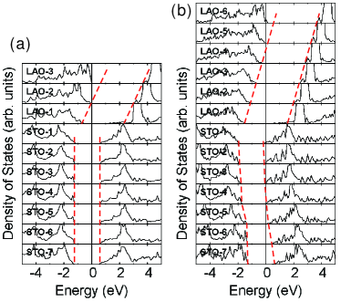
Figure 1 shows the layer-projected density-of-states (pDOS) of two representative systems with fully relaxed LAO layers: (a) (LAO)3/(STO)7 and (b) (LAO)6/(STO)7. The pDOS of the relaxed (LAO)3/(STO)7 exhibits an insulating band structure where the valence band maximum (VBM) of the LAO layers is set at the LAO surface layer. The dipole field in the LAO layers shifts the LAO band edges toward the higher energy relative to those of STO. The potential gradient is about 0.6 eV per layer for the relaxed structure, whereas it would be about 1.3 eV for the unrelaxed structure without polar distortions. It is noted that the VBM of the LAO surface layers, i.e., LAO-3 of Fig. 1(a) and LAO-6 of Fig. 1(b) deviates significantly from the extrapolated (dashed) lines connecting the VBM’s of its sub-surface layers. The lowering of the VBM of the LAO surface layer is attributed to its local environment being close to the bulk Al2O3 with a band gap larger than that of LAO. In addition to the surface effect, there also exists a band offset at the interface. There is a small but clear offset of about 0.5 eV between the LAO-1 and STO-1 layers, while the conduction band minimum (CBM) of the LAO-1 interface layer smears due to the hybridization between LaO and TiO2 layers.
The band edge shift in the LAO side reflects the change of electrostatic potential across the LAO overlayers. In Fig. 1, the layer-dependent potential profiles are marked by dashed lines. The gradient of the edge shift in (a) (LAO)3/(STO)7 is higher than that in (b) (LAO)6/(STO)7. From our calculations, in the system with in (LAO)m/(STO)7, the VBM of the surface LAO layer barely touches the CBM of the interface STO layer. When we have more than four LAO layers, the LAO/STO interface becomes metallic. As shown in Fig. 1(b) of the pDOS of the relaxed (LAO)6/(STO)7 structure, the charge carrier at the LAO/STO interface is induced as a result of charge transfer from the LAO surface. Despite that the potential gradient is reduced significantly by the polarization screening, the total potential shift across the LAO layers exceeds the STO band gap when the overlayer thickness goes over a critical value of 4 LAO layers. If the VBM of the surface LAO layer lies above the CBM of the interface STO layer, a charge transfer can occur between the LAO surface and the LAO/STO interface. From the results, we found that the total shift of the VBM is always delimited by the STO band gap for all . It implies that the potential shift is somehow compensated by the charge transfer. The polar distortion occurs in response to a local electric field, i.e., the potential gradient in the LAO layers, which in turn depends on the amount of charge transfer. Therefore, in order to determine the amount of charge transfer, it is necessary to understand the relation between the lattice polarization and the charge transfer.
In order to quantify the thickness dependence of the lattice polarization, we calculated the layer-by-layer polarization over the LAO layers as a functional of the LAO layer thickness. Polarization of the -th layer can be estimated by
| (1) |
where and are the Born effective charge and the displacement of the -th ion in the -th layer respectively, and is the volume of the LAO unit cell in the -th layer. Here we took the values of the Born effective charges from Ref. gemming06, . Since Eq. (1) can be used for the either La or Al cation-centered cells, we averaged out the contributions of the oxygens in the planes bounding the elementary unit cells nakhmanson05 .

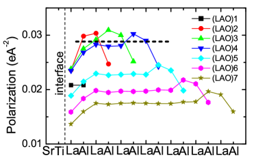
Figure 2 illustrates the profile of the layer-by-layer polarization over the LAO layers for (LAO)m/(STO)7 (). In all cases, it is noted that the polarizations of the interface and surface layers are significantly different from their average values. Although a reduction of the interface polarization may arise from both structural relaxation and charge screening, its origin may require a further investigation but is expected to be different from that of the ferroelectric insulator superlattices lee09 . Aside from the polarizations at the interface and surface layers, the average values of for , 3, and 4, denoted by a dashed line in Fig. 2, are roughly constant at about 0.03 e/Å2. From to 7, The average value of drops quickly as the layer thickness increases. This decrease of is related to the reduction of the potential gradient in the LAO layers, which is delimited by the STO band gap and the charge transfer between the surface and the interface.
For a given thickness for , since the potential shift in the LAO layers is delimited by the STO band gap, the local electric field can be approximated by where is a potential change corresponding to the STO band gap, and is an effective parameter corresponding to the dead layer contribution stengel06 . As the layer polarization is proportional to the local field , the inverse of the average polarization should satisfy the relation:
| (2) |
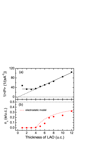
where is an average polarizability of the LAO layers. The -dependence of in Eq. (2) is clearly demonstrated in the plot of vs. as shown in Fig. 3(a). For , increases linearly in , while it remains constant below except for the case. The deviation of the polarization is not surprising because the single LAO layer consists of both surface and interface layers. From the least square fit to the calculated data, we could determine the effective parameter by where is the unit-cell thickness of the LAO layer.

For the metallic interface with , the potential shift, generated by the dipole field arising from the alternating stack of (LaO)+ and (AlO2)- charged layers, is screened by both lattice polarization and charge transfer. The relation between the interface (or surface) charge and the local electric field can be described in a simple electrostatic picture by the electric displacement field across the LAO overlayer: . If there is no free charge carrier at the interface, an average displacement field should correspond to as expected from the polarization catastrophe theory nakaga06 . When a charge transfer of occurs, however, the charge screening should give rise to . By combining the -dependence of and in Eq. (2), we obtain an expression for the -dependence of the induced charge carrier at the interface for :
| (3) |
where .
The calculated charge carriers density at the LAO/STO are shown in Fig. 3(b). For , the insulating interface has no charge carrier. At , where the VBM of LAO touches the CBM of STO, the carrier density is . For , increases monotonically as the thickness of the LAO overlayer grows. For the thin layers with , the carrier densities remain far less than 0.5 e/u.c.. From Eq. (3), it is obvious that e/u.c. can be achieved only when the LAO layers become extremely thick. By anchoring the coefficient to the value of at , we obtained . The fitting result based on the electrostatic model of Eq. (3) is displayed as a dashed line in Fig. 3(b). Despite of some discrepancy for the thin layers close to , the electrostatic model is found to be in a reasonable agreement with the DFT results. Considering that the electrostatic model is simplistic and may not be valid in the scale of a few atomic layers, this agreement is rather remarkable.

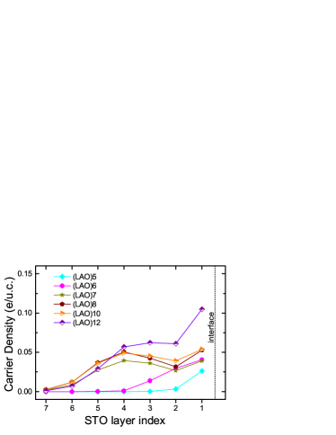
Although our electrostatic model explains the overall behavior of without oxygen vacancy, the induced charge carrier still depends on the detailed electronic structure near the interface. The charge carrier distribution at the interface is closely related to the band bending, i.e., the CBM edge shift in the STO substrate. When there is no charge carrier, i.e., , for the insulating interface with , no band bending occurs in the STO side as shown in Fig. 1(a). For the metallic interface with , on the other hand, the degree of the band bending depends on the amount of the charge carrier. In Fig. 4, we present the layer-resolved carrier distribution as a function of the LAO layer thickness. The induced charge carriers are found to be confined within 5 layers close to the LAO/STO interface, while the distribution for and 6 is even more localized within less than 3 layers. This result is in good agreement with a recent X-ray photo-electron spectroscopy (XPS) experiment, which reported that the carriers far less than 0.5 e/u.c. were found to be confined in one or a few layers of STO for thin LAO film without oxygen vacancy sing08 .
In conclusion, we explored a microscopic picture for the screening mechanism at the interface of the LAO overlayer on STO(001) by carrying out the DFT calculations, and demonstrated that the lattice polarization of the LAO layers is correlated with the carrier charge induced at the interface in terms of the overlayer thickness. Here we suggest an electrostatic model for the description of the charge carrier induced at the interface, where the detailed balance between the lattice polarization and the charge transfer plays a primary role when no oxygen vacancy or defect is present in the system. Although our discussion is restricted to the perfect lattice without defect, the electrostatic screening mechanism across the LAO overlayer should be considered as an alternative to the electronic reconstruction mechanism. We hope that our findings contribute to resolving the controversies on the origin and nature of the interface electron gas. In this picture, it is natural to observe a common lower limit of 0.03 electrons per u.c. for the systems with 4-to-5 LAO layers. In addition, one can consider the induced carrier density controlled by an external field, which affect the lattice polarization over the LAO layers.
This work was supported by the KOSEF through the ARP (R17-2008-033-01000-0). We also acknowledge the support from KISTI under the Supercomputing Application Support Program.
References
- (1) A. Ohtomo and H. Y. Hwang, Nature 427, 423 (2004).
- (2) N. Nakagawa, H. Y. Hwang, and D. A. Muller, Nature Mater. 5, 204 (2006).
- (3) A. Brinkman, M. Huijben, M. Van Zalk, J. Huijben, U. Zeitler, J. C. Maan, W. G. Van Der Wiel, G. Rijnders, D. H. A. Blank, and H. Hilgenkamp, Natural Mater. 6, 493(2007).
- (4) N. Reyren, S. Thiel, A. D. Caviglia, L. Fitting Kourkoutis, G. Hammerl, C. Richter, C. W. Schneider, T. Kopp, A.-S. Rütschi, D. Jaccard, M. Gabay, D. A. Muller, J.-M. Triscone, J. Mannhart, Science 317, 1196 (2007).
- (5) M. Basletic, J.-L. Maurice, C. Carrétéro, G. Herranz, O. Copie, M. Bibes, É. Jacquet, K. Bouzehouane, S. Fusil and A. Barthélémy, Nature Mater. 7, 621 (2008).
- (6) K. Yoshimatsu, R. Yasuhara, H. Kumigashira, and M. Oshima, Phys. Rev. Lett 101, 026802 (2008).
- (7) A. Kalabukhov, R. Gunnarsson, J. Börjesson, E. Olsson, T. Claeson, and D. Winkler, Phys. Rev. B 75, 121404 (2007).
- (8) G. Herranz, M. Basletić, M. Bibes, C. Carrétéro, E. Tafra, E. Jacquet, K. Bouzehouane, C. Deranlot, A. Hamzić, J.-M. Broto, A. Barthéléy, and A. Fert, Phys. Rev. Lett. 98, 216803 (2007).
- (9) W. Siemons, G. Koster, H. Yamamoto, W. A. Harrison, G. Lucovsky, T. H. Geballe, D. H. A. Blank, and M. R. Beasley. Phys. Rev. Lett. 98, 196802 (2007).
- (10) S. Thiel, G. Hammerl, A. Schmehl, C. W. Schneider, and J. Mannhart, Science 313, 1942 (2006).
- (11) S. Ishibashi, and K. Terakura, J. Phys. Soc. Jpn. 77, 104706 (2008).
- (12) R. Pentcheva and W. E. Pickett, Phys. Rev. Lett 102, 107602 (2009).
- (13) C. Cen, S. Thiel, G. Hammerl, C. W. Schneider, K. E. Andersen, C. S. Hellberg, J. Mannhart and J. Levy, Nature Mater. 7, 298 (2008).
- (14) M. Huijben, G. Rijnders, D. H. A. Blank, S. Bals, S. Van Aert, J. Verbeeck, G. Van Tendeloo, A. Brinkman, and H. Hilgenkamp, Nature Mater. 5, 556 (2006).
- (15) G. Kresse, and J. Furthmüller, Phys. Rev. B 54. 11169 (1996).
- (16) Y. Wang, J.P. Perdew, Phys. Rev. B 44, 13298 (1991).
- (17) P.E. Blöchl, Phys. Rev. B 50, 17953 (1994).
- (18) G. Kresse, and J. Joubert, Phys. Rev. B 59, 1758 (1999).
- (19) G. Makov and M.C. Payne, Phys. Rev. B 51, 4014 (1995).
- (20) K. Uchida and S. Tsuneyuki, Pyhs. Rev. B 68, 174107 (2003).
- (21) K. Janicka, J. P. Velev, and E. Y. Tsymbal, Phys. Rev. Lett. 102, 106803 (2009).
- (22) S. Gemming and G. Seifert, Acta Mater. 54, 4299 (2006).
- (23) S. M. Nakhmanson, K. M. Rabe, and D. Vanderbilt, Appl. Phys. Lett. 87, 102906 (2005).
- (24) J. H. Lee, J. Yu, and U. Waghmare, J. Appl. Phys. 105, 016104 (2009).
- (25) M. Stengel and N. A. Spaldin, Nature 443, 679 (2006).
- (26) M. Sing, G. Berner, K. Goß, A. Müller, A. Ruff, A. Wetscherek, S. Thiel, J. Mannhart, S. A. Pauli, C. W. Schneider, P. R. Willmott, M. Gorgoi, F. Schäfers, and R. Claessen, arXiv:0809.1917v1 (2008).