Spin polarized transport in semiconductors Rectification Spin-orbit coupling, Zeeman and Stark splitting, Jahn-Teller effect
Resonant tunneling-based spin ratchets
Abstract
We outline a generic ratchet mechanism for creating directed spin-polarized currents in ac-driven double well or double dot structures by employing resonant spin transfer through the system engineered by local external magnetic fields. We show its applicability to semiconductor nanostructures by considering coherent transport through two coupled lateral quantum dots, where the energy levels of the two dots exhibit opposite Zeeman spin splitting. We perform numerical quantum mechanical calculations for the - characteristics of this system in the nonlinear regime, which requires a self-consistent treatment of the charge redistribution due to the applied finite bias. We show that this setting enables nonzero averaged net spin currents in the absence of net charge transport.
pacs:
72.25.Dcpacs:
73.40.Eipacs:
71.70.Ej1 Introduction
The field of semiconductor spintronics has seen rapid progress lately, yet there are still many obstacles on the way from fundamental research to operating spin-based devices [1]. The creation of spin polarized currents is one basic requirement for the realization of semiconductor spintronics systems that share the prospect of being able to outperform conventional electronics. Due to a better controlability and faster processing times it is favorable to generate those currents by electrical means, e.g. by the variation of (contact) voltages. Promising classes of devices include spin pumps [2, 3, 4, 5], spin rectification [6] and spin ratchets [7, 8, 9, 10, 11, 12]. These proposals share the common idea to generate directed spin currents, e.g. mediated by spin-orbit interaction, upon time variation of external potentials. Here we focus on spin ratchets, a generalization of the particle quantum ratchet mechanism [13, 14, 15]. In such systems with broken spatial symmetry, pure spin currents are generated by means of an ac-driving with no net average bias. This idea has been put forward for both, nonlinearly driven coherent conductors [7, 8, 9], as well as conductors in the dissipative regime, where Brownian particle motion is converted into directed spin currents [10, 11, 12]. While a net spin current could be shown to exist for the different settings, its magnitude is difficult to predict and an optimization towards larger spin currents is often not evident.
Here we propose another, generic, spin ratchet mechanism that is based on coherent resonant charge and spin transfer. It thereby leads to larger and controllable output and can be implemented in a variety of systems. Moreover, since the ratchet spin currents require operation under nonequilibrium conditions and since the spin currents can usually be enhanced for strong ac-bias, we employ a fully self-consistent treatment of the electrostatics for our quantum transport calculations in the nonequilibrium regime. This involves a self-consistent determination of the voltage drop across the ratchet, which has been approximated so far only by simple heuristic models [7, 8, 9].
After outlining the general working principle we focus on a setup invoking resonant tunneling through two quantum dots (QD) in a two-dimensional electron gas (2DEG). In the literature double QD systems have already been proposed as spin filters [16, 17] or sources for pure spin currents [18]. However, these proposals are based on QDs in the Coulomb blockade regime, whereas the double QDs considered here are strong coupled to the leads, i.e. transport is fully coherent and the conductance is larger.
2 Mechanism
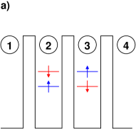
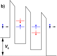
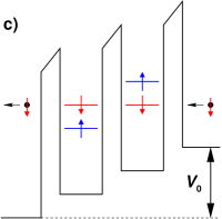
To illustrate the envisioned spin ratchet mechanism, let us first consider the simplified one-dimensional potential model shown in Fig. 1a). Three electrostatic barriers divide the system into four regions (R1-R4). While the regions R1 and R4 support states with a continuous energy spectrum, the regions R2 and R3, representing the double QD structure, accommodate discrete resonant states due to the confinement imposed by the barriers. We further assume a magnetic field oriented in opposite directions in R2 and R3. Thereby, the resonant energy levels in R2 and R3 are spin split due to the Zeeman coupling, however oppositely in both regions. A finite bias voltage across the device shifts the energy levels in R2 with respect to those in R3. This enables one to bring energy levels of the same spin state in the two QDs into resonance at a specific bias voltage, see Fig. 1b,c). For charge transport through the device, this results in an enhanced transmission of electrons of that specific spin state. Considering both forward and backward bias, it is obvious that the energy levels of different spin states can be brought into resonance for different signs of the bias voltage (see Fig. 1b,c)). Therefore, upon applying an ac-bias to the system, spin can be transported in the absence of a net charge current, as we will confirm below.
3 System and method
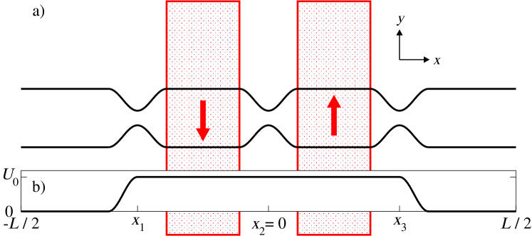
In Fig. 2 we depict a possible experimental setup, which takes advantage of the principle just described and can be realized with present day material processing techniques. It is based on a quantum wire (QW) patterned on a 2DEG in the -plane, see Fig. 2a. Within this wire (in -direction) which is connected to two non magnetic leads, two QDs possessing discrete energy levels are formed, e.g. via side gates. To realize the opposite Zeeman splitting inside these QDs, two ferromagnetic stripes (FMS) with opposite in-plane magnetization are patterned on top of the semiconductor heterostructure. The fringe fields of the FMS give rise to a non-uniform magnetic field in the plane of the 2DEG. We note that the proposed setup is just one possible realization of the mechanism to generate pure spin currents outlined in Fig. 1. Alternatively, one could for instance think of charge transport through resonant tunneling diodes, where the Zeeman splitting can be introduced, e.g., by layers of dilute magnetic semiconductors [19, 20].
The quantum dynamics of electrons in the conductor is described by the single-particle Hamiltonian
| (1) |
where is the effective mass, the effective gyroscopic factor, the Bohr magneton, and is the vector of the Pauli spin operators. Orbital effects due to the magnetic field are accounted for by the vector potential , which enters the momenta , while the Zeeman term couples the spin degree of freedom to the external magnetic field due to the FMS. For this setup can be evaluated – along with – using standard magnetostatics [21]. The potential includes the lateral confining potential which forms the QW and QDs, a possible potential offset due to an additional gate voltage (see Fig. 2b), as well as the electrostatic potential due to an applied (driving) bias voltage between the left and right contact to which the QW is connected. The driving is assumed to be adiabatic.
We neglect inelastic processes and assume phase coherent electron transport. The bias induces an electrical current, which we evaluate in the right lead. Specifically, the current of electrons with spin polarization (with respect to a quantization axis in direction) can be written as
| (2) |
Here denotes the energy of the conduction band edge, and is the difference between the Fermi functions in the two leads. In Eq. (2), the quantum transmission probability for electrons with spin is given by
| (3) |
where is the amplitude for transmission from the scattering state in the left lead into the scattering state in the right lead, with the summations running over the open transversal channels of the left/right lead. These amplitudes are evaluated by projecting the Green’s function of the open system onto an appropriate set of asymptotic spinors defining incoming and outgoing channels. Making use of a real-space discretization of the Schrödinger equation [22], the calculation of the -matrix elements was made feasible by the implementation of a recursive algorithm for the calculation of Green’s functions for spin-dependent transport [23].
4 Self-consistent numerical procedure
Since ratchet (spin) currents are expected for ac-driving with external bias voltages in the nonlinear regime, the profile of the electrostatic potential, dropping across the device, may play an important role for the working principle of the ratchet device, and hence its treatment needs special care. In the following we outline our approach to the non-equilibrium quantum transport problem including the self-consistent determination of the electrostatic potential drop arising from the charge rearrangement in the nonlinear bias regime. We consider the classical electrostatic potential described by the Poisson equation, , with for InAs. The charge density consists of both the density distributions of the electrons, , and the donors, . The latter is usually not known a priori, while the electron density can be calculated from the lesser Green function , see e.g. [22]:
| (4) |
In equilibrium the electrostatic potential is typically included in the effective confinement potential which we modelled by a hard-wall potential [24]. Therefore, the equilibrium electrostatic potential, governed by , with the electron density for zero-bias, need not be considered explicitly. Thus, in the nonequilibrium situation with a finite source-drain bias, only the change of the electrostatic potential due to the charge rearrangement of the electrons has to be included, similar as described in Ref. [25]. Hence the Poisson equation
| (5) |
has to be solved.
To account for the influence of the leads it is convenient to write the electrostatic potential as a sum, [25]. Here, is the potential induced by the contacts ignoring the charges in the device. It is the solution of the Laplace equation with boundary conditions , where is the distance between the contacts. For three-dimensional contacts, has the shape of a linear ramp. The contribution of the charges inside the system is described by , which is the solution of Eq. (5) with the boundary conditions of at the interfaces of the contacts.
If the electron density in the leads is substantially higher than in the device, the potential drop is screened in the leads leading to a flat electrostatic potential close to the contacts. Then, far from the device, and we can compute the electrostatic potential as
| (6) |
which is the solution of the Poisson equation for a vanishing potential at infinity.
For the self-consistent solution of the transport problem we compute from Eq. (4)the electron density for a given electrostatic potential and obtain an improved profile for the electrostatic potential from . It is known, however, that the straightforward iteration between Eqs. (4) and (6) typically does not converge [26]. Instead we adapted the Newton-Raphson method introduced in Refs. [26, 27] in order to evaluate the electrostatic potential by means of Eq. (6), which significantly improves the convergence behavior of the self-consistent computation scheme. After calculating the self-consistent electrostatic potential for each value of the source-drain voltage we are able to determine the transport properties of the considered ratchet device using Eq. (2).
5 Numerical results
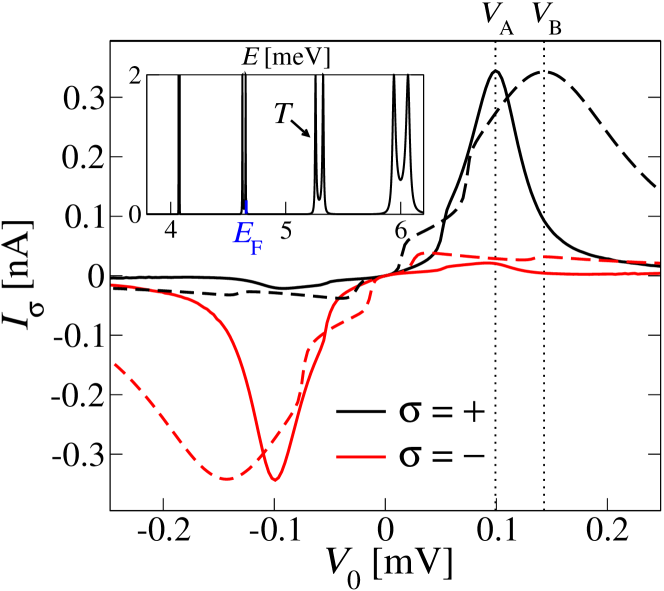
In the inset of Fig. 3 we show the transmission
in the linear-response regime, ,
at zero magnetic field for the device depicted in Fig. 2. The
system’s geometry parameters (specified in detail below) and energies are chosen such
that the leads carry 3 to 4 transversal modes,
while the point contacts only allow for (resonant) tunneling.
Thus, we find several sharp transmission peaks corresponding to
the discrete resonant energy levels of the two QDs. The peaks appear as
doublets due to the inter-dot tunnel splitting.
Upon applying a voltage we expect an asymmetric -
characteristic for the spin resolved currents for Fermi
energies close to those resonant energy levels.
To conduct explicit calculations for the spin current of the device
shown in Fig. 2 we have to fix several parameters. Taking InAs as
the material where the 2DEG is built from, we have and .
The width of the QW is chosen to be , while at the point contacts,
which are separated by , the width narrows down to . The two
FMS of identical size have dimensions , ,
and are centered on top of the two point contacts at a
distance above the 2DEG. For the magnetization of the
stripes we chose , a value well in
reach using e.g. Dysprosium [28].
To allow for a high electron density in the leads in order to screen the
electrostatic potential drop and to achieve a flat electrostatic potential
in R1 and R4, we include an additional confinement
potential as shown in Fig. 2b).
The spin-resolved - characteristics which are obtained with the described procedure for the Fermi energy at the second resonant energy level, meV (see inset of Fig. 3), are shown in Fig. 3 as solid lines (black and red line for spin-up and down, respectively). There we find that the device indeed acts as a spin selective current rectifier with dominant spin-up polarization for positive and spin-down polarization for negative bias voltages. This implies that when applying an adiabatically varying unbiased ac-voltage to the contacts the system only transports spins, yet no net charge, since the total charge currents average to zero. The pronounced maximum (minimum) at reflects level alignment, i.e. the resonance condition sketched in Fig. 1. For comparison the dashed lines in Fig. 3 represent the corresponding - curves arising from the aforementioned heuristic voltage drop model. It assumes a local voltage drop () at each of the three point contacts, i.e. the regions of maximum resistance. We find the same qualitative overall behavior for the spin currents, while the maximum of the resonant tunneling current is reached at a higher value, with being approximately three times the Zeeman splitting of the energy levels of the QD, as expected for this particular model. We performed further calculations (not presented here) which show that the degree of spin polarization, i.e. the efficiency of the device, increases with the Zeeman splitting in regions R2 and R3, due to the stronger separation of the spin energy levels at resonance for spin . Accordingly, the optimal working condition, i.e. levels for one spin species at resonance, is then reached at higher voltages.
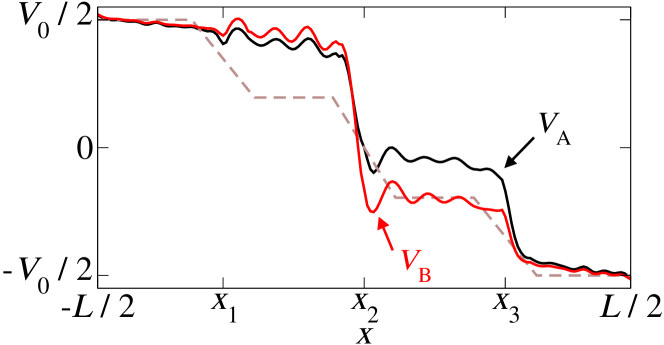
Since the amount of voltage that drops at the central point contact determines the alignment of the energy levels of the two QDs, in Fig. 4 we study the profile of the self-consistent electrostatic potential, , along the transport direction for applied bias (full black line) and (full red line) with marked in Fig. 3. We see that due to the point contacts a step structure emerges, with its exact form depending on and . Compared to the heuristic voltage drop model (dashed line), we find a stronger voltage drop at the central point contact. This explains that in Fig. 3 the current maximum is reached at lower bias voltages and the currents are significantly smaller at high bias for the self-consistent current calculation. Still, in view of Figs. 3 and 4, we can conclude that the heuristic voltage drop model constitutes a fair approximation to for the system considered.
6 Summary
In conclusion we have presented a generic mechanism to produce pure spin currents in nanostructures by applying an ac electrical bias. It is based on resonant transfer of spin-up and -down electrons in opposite directions and gives rise to pure ratchet type spin currents upon driving. Our results are based on self-consistent Keldysh Greens function transport in order to adequately describe the nonequilibrium condictions under which the system works.
Acknowledgements.
We acknowledge useful conversations with C. Ertler, M. Wimmer and D. Bercioux. The work was funded by the Deutsche Forschungsgemeinschaft within SFB 689. MS acknowledges additional funding from Studienstiftung des Deutschen Volkes.References
- [1] \NameAwschalom D. D. Flatté M. E. \REVIEWNat. Phys.32007153.
- [2] \NameMucciolo E. R., Chamon C. Marcus C. M. \REVIEWPhys. Rev. Lett.892002146802.
- [3] \NameWatson S. K., Potok R. M., Marcus C. M. Umansky V. \REVIEWPhys. Rev. Lett.912003258301.
- [4] \NameSharma P. Brouwer P. W. \REVIEWPhys. Rev. Lett.912003166801.
- [5] \NameGovernale M., Taddei F. Fazio R. \REVIEWPhys. Rev. B682003155324.
- [6] \NameBraunecker B., Feldman D. E. Li F. \REVIEWPhys. Rev. B762007085119.
- [7] \NameScheid M., Wimmer M., Bercioux D. Richter K. \REVIEWPhys. Status Solidi (c)320064235.
- [8] \NameScheid M., Pfund A., Bercioux D. Richter K. \REVIEWPhys. Rev. B762007195303.
- [9] \NameScheid M., Bercioux D. Richter K. \REVIEWNew J. Phys.92007401.
- [10] \NameSmirnov S., Bercioux D., Grifoni M. Richter K. \REVIEWPhys. Rev. Lett.1002008230601.
- [11] \NameSmirnov S., Bercioux D., Grifoni M. Richter K. \REVIEWPhys. Rev. B782008245323.
- [12] \NameSmirnov S., Bercioux D., Grifoni M. Richter K. arXiv:0903.2765v1 (unpublished) (2009).
- [13] \NameReimann P., Grifoni M. Hänggi P. \REVIEWPhys. Rev. Lett.79199710.
- [14] \NameLinke H., Humphrey T. E., Lofgren A., Sushkov A. O., Newbury R., Taylor R. P. P. Omling \REVIEWScience28619992314.
- [15] \NameHänggi P. and Marchesoni F. \REVIEWRev. Mod. Phys.812009387.
- [16] \NameCota E., Aguado R., Creffield C. E. Platero G. \REVIEWNanotechnology142003152.
- [17] \NameCota E., Aguado R. Platero G. \REVIEWPhys. Rev. Lett.942005107202.
- [18] \NameSun Q.-f., Guo H. Wang J. \REVIEWPhys. Rev. Lett.902003258301.
- [19] \NameSlobodskyy A., Gould C., Slobodskyy T., Becker C. R., Schmidt G. Molenkamp L. W. \REVIEWPhys. Rev. Lett.902003246601.
- [20] \NameErtler C. Fabian J. \REVIEWAppl. Phys. Lett.892006242101.
- [21] \NameJackson J. \BookClassical Electrodynamics (John Wiley & Sons, Inc.) 1999.
- [22] \NameFerry D. K. Goodnick S. M. \BookTransport in Nanostructures (Cambridge University Press) 1997.
- [23] \NameLassl A., Schlagheck P. Richter K. \REVIEWPhys. Rev. B752007045346.
- [24] \NameLaux S. E., Frank D. J. Stern F. \REVIEWSurf. Sci.1961988101.
- [25] \NameXue Y., Datta S. Ratner M. A. \REVIEWChem. Phys.2812002151.
- [26] \NameTrellakis A., Galick A. T., Pacelli A. Ravaioli U. \REVIEWJ. Appl. Phys.8119977880.
- [27] \NameLake R., Klimeck G., Bowen R. C. Jovanovic D. \REVIEWJ. Appl. Phys.8119977845.
- [28] \NameUzur D., Nogaret A., Beere H. E., Ritchie D. A., Marrows C. H. Hickey B. J. \REVIEWPhys. Rev. B692004241301.