DFT study of graphene antidot lattices: The roles of geometry relaxation and spin
Abstract
Graphene sheets with regular perforations, dubbed as antidot lattices, have theoretically been predicted to have a number of interesting properties. Their recent experimental realization with lattice constants below 100 nanometers stresses the urgency of a thorough understanding of their electronic properties. In this work we perform calculations of the band structure for various hydrogen-passivated hole geometries using both spin-polarized density functional theory (DFT) and DFT based tight-binding (DFTB) and address the importance of relaxation of the structures using either method or a combination thereof. We find from DFT that all structures investigated have band gaps ranging from 0.2 eV to 1.5 eV. Band gap sizes and general trends are well captured by DFTB with band gaps agreeing within about 0.2 eV even for very small structures. A combination of the two methods is found to offer a good trade-off between computational cost and accuracy. Both methods predict non-degenerate midgap states for certain antidot hole symmetries. The inclusion of spin results in a spin-splitting of these states as well as magnetic moments obeying the Lieb theorem. The local spin texture of both magnetic and non-magnetic symmetries is addressed.
pacs:
73.63.Fg, 73.63.-bI Introduction
Graphene, the single-atom thick two-dimensional sheet of carbon atoms, has stimulated considerable experimental Geim and Novoselov (2007) and theoretical research Katsnelson et al. (2006) as well as proposals for future nanodevicesAvouris et al. (2007). Various graphene-based applications have been realized in recent yearsNovoselov et al. (2005); Novoselov and Geim (2007) and the relevance for application in devices is heavily increased by the rapidly improving ability to pattern monolayer films with e-beam lithography Geim and Novoselov (2007) where features on the ten-nm scale have been obtained Han et al. (2007); Fischbein and Drndi c (2008). Moreover, recent advances in chemical vapor deposition of graphene (see e.g. Ref. [Kim et al., 2009]) are promising for fabrication of large area, high quality devices.
Yet another way of nanoengineering graphene consists of defining an antidot lattice on graphene by means of a regular array of nanoscale perforations. This theoretical idea was introduced by Pedersen et al. Pedersen et al. (2008a, b), who showed using tight-binding calculations that antidot lattices change the electronic properties from semimetallic to semiconducting with a significant and controllable band gap. Such structures have recently been realized experimentally by Shen et al. Shen et al. (2008) and Eroms et al. Eroms and Weiss with lattice spacings down to 80 nm. Quantum dots and graphene ribbons have been demonstrated with dimensions of only a few nm Ritter and Lyding (2009). Very recently, Girit et al. Girit et al. (2009) have studied the dynamics at the edges of a growing hole in real time using a transmission electron microscope. Both in the experiment and in Monte Carlo simulations they find the zig-zag edge formation to be the most stable structure. This is in agreement with the findings of Jia et al.Jia et al. (2009) who demonstrate a method to produce graphitic nanoribbon edges in a controlled manner via Joule heating. This opens the possibility of making antidot lattices with a desired hole geometry.
While carbon nanotubes, graphene and recently graphene ribbons have been studied extensively using first principles methods, antidot lattices in graphene have mainly been treated with simpler modelsPedersen et al. (2008a); Vanevic et al. . The very recent work by Vanevic et al. Vanevic et al. uses a -orbital tight-binding model to study antidot lattices with rather large lattice constants (these systems are more easily accessed experimentally but cannot be analyzed in terms of ab initio methods). Their focus is on the possible occurrence of midgap states without introducing defects in the antidot lattice, as was the case in the original proposal by Pedersen et al.
Many studies on magnetization have been reported for various graphene structuresLieb (1989); Lehtinen et al. (2004); Palacios et al. (2008); Kumazaki and Hirashima (2008); Jiang et al. (2007); Philpott et al. (2008). The origin of the magnetism can be understood based on the theory by Lieb Lieb (1989), and the subsequent related work by Inui et al. Inui et al. (1994) on the properties of the bipartite lattice. Single vacancies and their spin properties have been studied by, e.g. Lehtinen et al. Lehtinen et al. (2004) and Palacios et al.Palacios et al. (2008); the latter paper also investigates voids in both graphene and graphene ribbons in detail using a mean-field Hubbard-model. Magnetization has also been studied in carved slitsKumazaki and Hirashima (2008), finite ribbonsJiang et al. (2007) and flakes Jiang et al. (2007); Philpott et al. (2008) as well as rings Bhamon et al. (2009) and notches Hancock et al. (2008). Recently, DFT treatments of magnetic properties of nano-holes in grapheneYu et al. (2008) and graphene films Chen et al. (2008) have been published.
The realized antidot lattices with hole sizes of several tens of nanometers and even larger lattice spacings involve several thousands of atoms in a unit cell and are computationally too costly to be treated with DFT in a systematic manner. The DFT based tight-binding method, DFTB Porezag et al. (1995), however, allows one to address such large systems. The difference in computational cost between DFT and DFTB is for the present study found to be at least a factor of thirty. We thus investigate the accuracy of DFTB compared to DFT on much smaller antidot lattices in terms of the band structures111We note, that DFT is known to underestimate the band gap, see, e.g. M.S.Hybertsen and S.G. Louie, Phys. Rev. B 34, 5390 (1986).. Since geometry relaxation is the most costly task in DFT we also investigate the cost benefits of combining the two methods. By using DFT and elaborating on the role of spin, we also wish to address some of the main features found specifically for antidot lattices on a tight-binding level of the theory.
This paper is organized as follows. In Sec. II we introduce the antidot lattice systems and the methods used. The equilibrium geometries and band structures obtained using both DFT and DFTB and a combination thereof is given in Sec. III together with a detailed investigation of the spin properties. We conclude with a short summary.
II Systems and Method
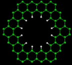
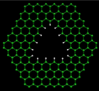
The specific realization of the antidot lattice we consider in this paper is a hexagonal (triangular) array of holes in a graphene sheet as proposed by Pedersen et al. Pedersen et al. (2008a). Within the hexagonal unit cells there can be different hole geometries, and two examples of high symmetry holes are shown in Fig. 1. Below, geometries are fully relaxed but as a starting point ideal geometries using fixed bond lengths and angles of are constructed. These geometries furthermore provide a straightforward notation for the structures. Thus, we designate antidot lattices with circular holes according to the notation , where is the side length of the unit cell and the hole radius, both measured in units of the graphene lattice constant =2.46 Å giving a C-C bond length of 1.42 Å. Similarly, for triangular holes, we apply the notation , where denotes the side length of the hole Vanevic et al. . The holes are passivated with H using a C-H bond length of 1.1 Å and consist almost entirely of zig-zag edges. These structures are idealized but may well be within experimental reach given the recent advancements Girit et al. (2009); Jia et al. (2009).
For the first principles calculations we have used the ab initio pseudopotential DFT as implemented in the Siesta codeSoler et al. (2002) to obtain the electronic structure and relaxed atomic positions from spin-polarized DFT222The systems are relaxed using the conjugate gradient (CG) method with a force tolerance of 0.01 eV/Å. All atoms are allowed to move during relaxation but the unit cell is kept fixed with a vacuum between graphene layers in neighboring cells of 10 Å. The mesh cutoff value defining the real space grid used is 175 Ry and we employ a double- polarized (DZP) basis set. A Monkhorst-Pack grid of (2,2,1) was found sufficient for all structures. . We employ the GGA PBE functional for exchange-correlationPerdew et al. (1996).
For the DFTB results333We relax the two outermost rows of atoms along the perimeter of the hole until the total energy per atom was converged to better than eV., we use the original (C,H) parametrization of Porezag et al.Porezag et al. (1995) which does not include spin.
III Results
| DFT | Non-spin DFT | DFTB | ||||
| Relaxation | None | DFT | DFTB | DFTB | None | DFTB |
| 0.93 | 1.01 | 0.97 | 0.97 | 0.99 | 1.05 | |
| 0.72 | 0.84 | 0.79 | 0.79 | 0.88 | 0.98 | |
| 1.27 | 1.51 | 1.35 | 1.35 | 1.72 | 1.74 | |
| 0.39 | 0.52 | 0.46 | 0.46 | 0.65 | 0.75 | |
| 0.24 | 0.22 | 0.22 | 0.00 | 0.00 | 0.00 | |
For all considered structures a structural relaxation with DFT leads to a shrinking of the hole, of the order of 1 %, resulting in C-C bonds close to the edges stretching and contracting in the range of 1.39 - 1.45 (1.43 for ) Å. A few bond lengths away from the hole edge the C-C bond length remains unaltered at 1.42 Å.
In the case of relaxation with DFTB the picture is quite similar. Edge-atom C-C bond lengths vary from 1.39-1.42 Å for all systems but , which has variations of 1.38 - 1.44 Å. The shrinking of the hole size is smaller than 1%.
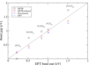
The results for the band gaps for five different systems are summarized in Table 1. The band structures are calculated using both DFT and DFTB on structures relaxed at different accuracy levels and thus at different computational costs. The combinations are not exhaustive but represent a relevant set aimed at saving computational costs. The relaxation type is given in the second row of Table 1. DFTB is expected to match DFT better as increases due to decreased importance of edge details. The systems chosen here are mostly edge-dominated (low ratio) and thus represent the worst case scenario.
Using DFT we find band gaps ranging from 0.2 to 1.5 eV confirming that the antidot lattice turns the semimetallic graphene into a semiconductor Pedersen et al. (2008a). However, only spin-polarized DFT predicts a band gap for the structure which will be discussed in detail below.
Pedersen et al. Pedersen et al. (2008a) demonstrated a scaling-law between the hole size and the band gap for large ratios but no such simple picture for small ratios emerged. This trend agrees well with our edge-dominated systems were no simple scaling between the hole size and the band gap could be identified.
As illustrated on Fig. 2, DFTB in general gives a larger band gap than DFT (the circles lie consistently above the dashed line). This tendency is enhanced the more edge-like the structure becomes. On average, the DFTB gap is 20% larger than the DFT value for the four structures with circular perforations. The discrepancy increases for structures with holes occupying a large portion of the unit cell, such as . Moreover, for the omission of spin effects leads incorrectly to a vanishing DFTB band gap in agreement with non-spin DFT. In the cases of the and systems the band structures are shown in Fig. 3 left and right, respectively, calculated using DFT (DFTB) in the upper(lower) panel. We see that the shape of the bands corresponds qualitatively for the two methods.
III.1 Relaxation
We next analyze the importance of relaxation. The clear trend is that relaxation increases the band gap. This is illustrated for DFT in Fig. 2 (crosses corresponding to the unrelaxed structure lie below the dotted line), as well as in Table 1 for DFTB. Comparing unrelaxed results with fully relaxed results we see from Table 1 a change in band gaps within 10 % and 15 % using DFTB and DFT, respectively. Only in the case of DFT does the effect of relaxation increase the more edge-dominated the system becomes. The change using DFT for the system is 8 % compared to 16 % for .
It must be emphasized that larger differences between initial and relaxed geometries may well give rise to a larger discrepancy between their band gaps. However, even for the case of a single passivated edge-defect the difference in relaxed and unrelaxed DFT band gaps is less than 10 %.
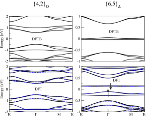
By relaxing the geometry with DFTB the DFT results are improved from the non-relaxed case as shown in Fig. 2 (the squares are closer to the dashed line than the crosses). Compared to pure DFT the largest difference in the band gap is again found for the edge-dominated system: it is now 11 % compared to 16 % without relaxation. For the larger structure we find the same values as for pure DFT. The DFT results are shown for both DFT-relaxed and DFTB-relaxed structures on Fig. 3 indicated by thick and dotted line, respectively. The different geometries do not change the bands notably.
Using DFT on DFTB-relaxed structures is thus an approach with a good trade-off between accuracy and computational cost. This finding is of great practical use, since relaxation is very costly in DFT.
III.2 Magnetic properties
For the system with both non-spin-DFT and DFTB there are
three (one nearly doubly degenerate) bands with weak dispersion at
zero energy. Introducing spin leads to a clear splitting of these
bands, i.e., to the formation of a band gap. For a comparison of
DFT and DFTB, see Fig. 3, right column. The three bands
below (above) the Fermi level are half-filled by majority (minority)
spin electrons and are thus completely spin-polarized. The size of
the band gap is thus also an indication of the robustness of the
magnetic
state Kusakabe and Maruyama (2003).
The magnetic moments of the structures can be understood as a consequence of graphene being a bipartite lattice in the nearest neighbor approximation as shown by Lieb Lieb (1989). According to Lieb’s theorem Lieb (1989), the total magnetic moment can be written as where is the number of atoms occupying the sites of the bipartite graphene lattice. Thus, if the angle between the zigzag edges is or the edge-atoms belong to the same sublattice, while they belong to different sublattices if the angle is or . Consequently, the hexagonal hole is non-magnetic and the triangular is magnetic. This is consistent with a Mulliken analysis from the DFT calculations which shows a non-zero magnetic moment only for the system of 3.00 per unit cell. By inspection of the geometry we indeed find =3.
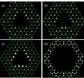
As a continuation of Lieb’s work, Inui et al. Inui et al. (1994) showed that such sublattice imbalance results in there being midgap states with zero energy. We thus expect a degeneracy of 3 of the low-dispersion bands in the case.
In Fig. 3, lower right panel, there is one largely dispersionless band just below two almost completely degenerate bands which have some dispersion especially at the -point. Such band curvature was also found for hydrogenated graphene ribbons by Kusakabe et al. Kusakabe and Maruyama (2003) The -point states for each band are shown in Fig. 4, where the strong localization is seen for the lowest band, Fig. 4(c), whereas the bands with curvature, Fig. 4(a,b), yield less localized states. Note also the alternation in the amplitudes of the states between sublattices as proposed by Inui et al. Inui et al. (1994) The state of the highest occupied (spin-degenerate) band for the non-magnetic structure is shown for comparison in Fig. 4(d). The splitting as well as the curvature is less pronounced for the unfilled states above the Fermi level showing particle-hole asymmetry. This asymmetry is expected due to the breaking of the symmetry of the bipartite lattice partly due to the DFT treatment beyond nearest neighbor as well as the passivation of the edges which changes the on-site potential at edge-sites. This is inherently also the case for DFTB. By inspection of the SIESTA HamiltonianSoler et al. (2002) we find an increase in on-site energy for passivated edge atoms as compared to atoms far from the edge. Vanevic et al. Vanevic et al. find that a potential shift on the edge-atoms mainly causes a lifting of the degeneracy of the flat bands, consistent with our observations.
As mentioned above, the global spin is given by the sublattice imbalance. This does not, however, determine the local spin. For the hexagonally shaped hole structures we find not only a zero global spin, but also a zero spin on all atoms. This explains the identical band gaps found using DFT with and without spin. Such non-magnetic solutions have been found for finite graphene ribbons or graphene flakes by Jiang et al. Jiang et al. (2007) using DFT. They find a sudden transition from non-magnetic to magnetic solutions going from a system size of [3,3] and [4,3] with numbers indicating rings in the graphene lattice along zig-zag and armchair directions. Such transitions are also seen in slits cut in graphene in a study by Kumazaki et al. Kumazaki and Hirashima (2008) Viewing each edge in our hexagonal structures as ribbons, the largest ribbon corresponds to a [4,3] ribbon ( structure). We thus expect local magnetization to appear for slightly larger systems.
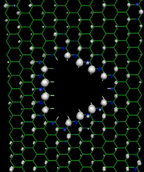
For we have the strongest polarization at the middle of each edge with maximum magnetic moment per atom being 0.24 . We note that each corner atom has a magnetization -0.03 . The edge atom magnetization is below the maximum of 1/3 for graphene ribbons when the width becomes too large for edge-edge interactions. Our systems thus have edge-edge interactions which is expected due to the ribbon width of 6 rings. A plot of the spin-polarized density444Due to the larger cell used in this calculation we use less accurate settings (single- basis, 100 Ry mesh, one -point). This changes the magnitude of the spin somewhat as compared to the smaller cell calculations. The maximum magnetic moment per atom is 0.27 for the large cell versus 0.24 for the smaller. The qualitative picture of the spin distribution is, however, the same for both calculations. is shown in Fig. 5. The majority spins reside mostly on the edges of the dominant sublattice sites. Neighboring sites on the other sublattice have minority spin-polarization. Note also the non-zero spin of the atoms far from the edges indicating interaction between neighboring hole-edges.
IV Conclusion
Using DFT and DFTB we have calculated band gaps in various antidot lattice geometries. The computed band gaps range from 0.2 to 1.5 eV. In general, DFTB gives larger band gaps than DFT with the largest difference for non-magnetic structures of 44 %. Geometry relaxation using either method is found to increase the band gap with maximally 15%. Combining the two methods by performing a DFT-calculation on a DFTB-relaxed structure is found to give a good trade-off between accuracy and computational cost facilitating the treatment of larger systems. However, even for unrelaxed geometries we find qualitative agreement with the DFT-relaxed geometries. Trends for ideal geometries as presented here can thus be investigated without any relaxation in the non-magnetic case.
Certain geometries are shown with DFT to have a non-zero total magnetic moment which is understood via Lieb’s theorem as a consequence of sublattice imbalance. For these structures a spin-polarized treatment is needed to achieve even qualitative results for the band gaps. Local spin, which can occur regardless of the total magnetic moment, is not observed for very edge-dominated systems. Sublattice imbalance leads to the occurrence of low-dispersion midgap bands. We find a lifting of degeneracy of these otherwise degenerate bands on a perfect bipartite lattice as well as a considerable spin-splitting. These completely spin-polarized states are primarily located at the hole-edges.
Acknowledgements.
We thank Jesper G. Pedersen for fruitful discussions. Financial support from Danish Research Council FTP grant ’Nanoengineered graphene devices’ is gratefully acknowledged. Computational resources were provided by the Danish Center for Scientific Computations (DCSC). APJ is grateful to the FiDiPro program of the Finnish Academy.References
- Geim and Novoselov (2007) A. Geim and K. Novoselov, Nature Materials 6, 183 (2007).
- Katsnelson et al. (2006) M. I. Katsnelson, K. S. Novoselov, and A. K. Geim, Nature Physics 2, 620 (2006).
- Avouris et al. (2007) P. Avouris, Z. Chen, and V. Perebeinos, Nature Nanotechnology 2, 605 (2007).
- Novoselov et al. (2005) K. S. Novoselov, A. K. Geim, S. V. Morozov, D. Jiang, M. I. Katsnelson, I. V. Grigorieva, S. V. Dubonos, and A. A. Firsov, Nature 438, 197 (2005).
- Novoselov and Geim (2007) K. Novoselov and A. Geim, Materials Technology 22, 178 (2007).
- Han et al. (2007) M. Y. Han, B. Ozyilmaz, Y. B. Zhang, and P. Kim, Physical Review Letters 98, 206805 (2007).
- Fischbein and Drndi c (2008) M. D. Fischbein and M. Drndi c, Applied Physics Letters 93, 113107 (2008).
- Kim et al. (2009) K. S. Kim, Y. Zhao, S. Y. Lee, J. M. Kim, K. S. Kim, J.-H. Ahn, P. Kim, J.-Y. Choi, and B. H. Hong, Nature 457, 706 (2009).
- Pedersen et al. (2008a) T. G. Pedersen, C. Flindt, J. Pedersen, N. A. Mortensen, A. P. Jauho, and K. Pedersen, Physical Review Letters 100, 136804 (2008a).
- Pedersen et al. (2008b) T. G. Pedersen, C. Flindt, J. Pedersen, A. P. Jauho, N. A. Mortensen, and K. Pedersen, Physical Review B 77, 245431 (2008b).
- Shen et al. (2008) T. Shen, Y. Q. Wu, M. A. Capano, L. P. Rokhinson, L. W. engel, and P. D. Ye, Applied Physics Letters 93, 122102 (2008).
- (12) J. Eroms and D. Weiss, arxiv.0901.0840v1.
- Ritter and Lyding (2009) K. A. Ritter and J. W. Lyding, Nature Materials 8, 235 (2009).
- Girit et al. (2009) C. O. Girit, J. C. Meyer, R. Erni, and M. D. Rossel, Science 323, 1705 (2009).
- Jia et al. (2009) X. Jia, M. Hofmann, V. Meunier, B. G. Sumpter, J. Campos-Delgado, J. M. Romo-Herrera, H. Son, Y.-P. Hsieh, A. Reina, J. Kong, et al., Science 323, 1701 (2009).
- (16) M. Vanevic, V. M. Stojanovic, and M. Kindermann, arxiv.0903.0918v1.
- Lieb (1989) E. H. Lieb, Physical Review Letters 62, 1201 (1989).
- Lehtinen et al. (2004) P. Lehtinen, A. Foster, Y. Ma, A. Krasheninnikov, and R. Nieminen, Phys. Rev. Lett. 93, 187202 (2004).
- Palacios et al. (2008) J. J. Palacios, J. Fernandez-Rossier, and L. Brey, Physical Review B 77, 195428 (2008).
- Kumazaki and Hirashima (2008) H. Kumazaki and D. S. Hirashima, Low Temperature Physics 34, 805 (2008).
- Jiang et al. (2007) D. E. Jiang, B. G. Sumpter, and S. Dai, Journal Of Chemical Physics 127, 124703 (2007).
- Philpott et al. (2008) M. R. Philpott, F. Cimpoesu, and Y. Kawazoe, Chemical Physics 354, 1 (2008).
- Inui et al. (1994) M. Inui, S. A. Trugman, and E. Abrahams, Physical Review B 49, 3190 (1994).
- Bhamon et al. (2009) D. Bhamon, A. Pereira, and P. Sculz, Phys. Rev. B 89, 125414 (2009).
- Hancock et al. (2008) Y. Hancock, K. Saloriutta, A. Uppstu, A. Harju, and M. Puska, J Low Temp Phys 153, 393 (2008).
- Yu et al. (2008) D. Yu, E. Lupton, M. Liu, and F. Liu, Nano Res 1, 56 (2008).
- Chen et al. (2008) Y. P. Chen, Y. E. Xie, and X. H. Yan, Journal Of Applied Physics 103, 063711 (2008).
- Porezag et al. (1995) D. Porezag, T. Frauenheim, T. Kohler, G. Seifert, and R. Kaschner, Physical Review B 51, 12947 (1995).
- Soler et al. (2002) J. M. Soler, E. Artacho, J. D. Gale, A. Garcia, J. Junquera, P. Ordejon, and D. Sanchez-Portal, Journal Of Physics-Condensed Matter 14, 2745 (2002).
- Perdew et al. (1996) J. P. Perdew, K. Burke, and M. Ernzerhof, Phys. Rev. Lett. 77, 3865 (1996).
- Kusakabe and Maruyama (2003) K. Kusakabe and M. Maruyama, Physical Review B 67, 092406 (2003).