Spin-polarized transport through domain wall in magnetized graphene
Abstract
Atomically thin two-dimensional layer of honeycomb crystalline carbon known as graphene is a promising system for electronics. It has a point-like Fermi surface, which is very sensitive to external potentials. In particular, Zeeman magnetic field parallel to the graphene layer splits electron bands and creates fully spin-polarized and geometrically congruent circular Fermi surfaces of particle and hole type. In the presence of electric field, particles and holes with opposite spins drift in opposite direction. These phenomena are likely to be of interest for developing graphene-based spintronic devices. A domain wall (DW) separating regions with opposite spin polarizations is a basic element of such a device. Here we consider a ballistic passage of spin-polarized charge carriers through DW in graphene. We also discuss the analogy between the generation of spin currents in graphene and in relativistic quark-gluon plasma, where the spin-polarized current is responsible for the phenomenon of charge separation studied recently at RHIC.
pacs:
73.63.-nb, 73.40.-c, 72.25.-b, 75.25.MkI Introduction
The remarkable properties of graphene GeimNovoselov_NatMat2007 at present attract attention of many researchers. Its honeycomb two-dimensional (2D) crystalline order is extremely robust. In view of the well-known Peierls-Landau argument proving the thermodynamical instability of isolated 2D crystals LandauLifshitz , robustness of graphene monolayers may look somewhat surprising. While graphene sheets in natural and synthetic graphite materials are not isolated but are supported on 3D substrates OshimaNagashima_JPCM1997 ; Forbeaux_PRB1998 , binding of the monolayers is so weak that they can be easily exfoliated and in many cases appear approximately isolated from the substrate Forbeaux_PRB1998 ; Novoselov_PNAS2005 ; Charrier_JAP2002 ; Ohta_PRL2007 .
Adding to the enthusiasm were recent discoveries of exceptionally high electronic quality of graphene monolayers Novoselov_Science2004 ; Berger_Science2006 . Carefully prepared samples show ambipolar electric field effect with carrier mobilities exceeding cm2/V/s for electron/hole concentrations up to cm. Novoselov_Science2004 ; Berger_Science2006 High quality graphene samples at present can be obtained either by using graphite exfoliation, which results in graphene pieces with 1 to 100 m linear dimensions GeimNovoselov_NatMat2007 , or by epitaxial growth on SiC via silicon sublimation, which yields macroscopic mosaic layer with micron-size crystalline domains Hass_APL2006 .
High electron mobility implies ballistic charge transport and electronic phase coherence on the micron length scale, which is comparable with high-quality semiconductor heterostructures traditionally used for the studies of the quantum Hall effect (QHE) Tsui_etal_PRL1982 . Moreover, charge mobilities in graphene are only weakly temperature dependent, being probably limited by sample imperfections and size effects even at room temperature GeimNovoselov_NatMat2007 . Hence, not only QHE was indeed observed in graphene Novoselov_Nature2005 ; Zhang_Nature2005 , but it was also found to survive up to 300 K Novoselov_Science2007 , indicating that the electrons in graphene form a quantum gas even at room temperature.
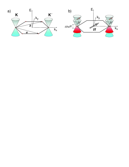
The exceptional electronic properties of graphene such as high charge carrier mobility, long mean free path and coherence length and ability to support high current densities, exceeding A/cm2, Novoselov_Science2004 make it a promising candidate for nano-scale electronics. In addition, its unique electronic structure provides a playground for the studies of (2+1)-dimensional (space+time) quantum electrodynamics. The crossing of the energy bands associated with two different sub-lattices and of the graphene’s honeycomb crystal lattice results in the energy spectrum of electron and hole quasi-particles, which is linear in momentum [see Fig 1(a)], , where is the Fermi velocity. This has been observed experimentally in transport measurements Novoselov_Nature2005 ; Zhang_Nature2005 and in angle-resolved photoemission Ohta_PRL2007 .
A gapless linear 2D spectrum of electron and hole quasi-particles belonging to two sublattices implies that charge carriers in graphene can be formally described as two-dimensional relativistic chiral fermions with spin and with pseudo-spin accounting for the two-sublattice band structure. A straightforward consequence is the conservation of the pseudo-spin chirality of the quasiparticles defined as the pseudo-spin projection on the momentum, . The orbital motion in magnetotransport and QHE experiments can be described by the “truncated” 2D Dirac equation for massless fermions Novoselov_Nature2005 ; Zhang_Nature2005 ; Novoselov_Science2007 ,
| (1) |
where are Pauli matrices acting in the pseudo-spin space. They account for the two-sublattice nature of graphene’s honeycomb lattice and the resulting composite structure of the dispersion cone around each of the Fermi points. is a rank two spinor wavefunction and is the 2D momentum operator Khveshchenko ; GorbarGusynin_PRB2002 ; DeMartino_PRL2007 .
Eq. (1) assumes degeneracy with respect to spin and valley indices, which are taken into account simply by multiplying the number of states by 4. Spin degeneracy is usually justified by the fact that typical Zeeman electronic level splitting induced by the laboratory magnetic field is indeed very small. However, when magnetic field is applied parallel to the plane of graphene, orbital motion and Landau quantization are irrelevant and it is the lifting of spin and valley degeneracies that becomes important Aleiner_PRB2007 . Such situation is in fact of immediate interest for possible spintronic applications, which employ the spin degree of freedom of Dirac fermions in graphene. With recent measurements showing spin coherence scale in graphene exceeding 1m Tombros_Nature2007 , there is a growing recognition of the potential of this approach Tombros_Nature2007 ; Cho_APL2007 ; Hill_IEEE2006 . Moreover, it can be envisioned that spin-dependent splitting of the electronic levels in graphene could be induced by an effective magnetic field resulting from magnetic proximity effect in graphene in contact with a ferro/antiferromagnetic substrate patent ; Haugen_2007 . Such “exchange” field acts only in the spin sector and can be much stronger than magnetic fields available in the laboratory, inducing level splitting sufficient for room-temperature device applications.
Here we consider transport of chiral Dirac fermions in graphene in the presence of such an in-plane magnetic field and their passage through a boundary between two regions with different field orientations. The latter might be associated with a domain wall in the magnetic layer of graphene-magnet (GM) heterostructure, and presents a basic element for spintronic applications.
II Effect of parallel magnetic field
When external magnetic field is applied to graphene, its parallel component acts only on spin degree of freedom, while the perpendicular component couples both to spin and to the orbital motion as described by Eq. (1). Hence, the action of the parallel field is equivalent to band splitting by the “exchange field” arising from magnetic proximity effect induced by the magnetic substrate. Such proximity-induced field, regardless of its direction, does not couple to the orbital motion.
Point-like Fermi surface makes electronic properties of graphene extremely sensitive to external potentials. Experiments show that application of a moderate gate voltage results in an appearance of finite charge carrier density, which is proportional to the magnitude of applied electric field. The type of these induced carriers, revealed by the sign of the Hall effect, depends on the polarity of the gate voltage GeimNovoselov_NatMat2007 ; Novoselov_Nature2005 . This can be easily visualized by considering the electronic spectrum in graphene shown in Fig. 1(a), where the Fermi level is shifted by applying the gate voltage, thus inducing a circular Fermi-surface of particle or hole type, depending on the polarity.
External magnetic field splits electronic band structure in graphene according to spin. Chemical potential for one spin polarization is increased by the amount equal to Zeeman energy , while for the other it is decreased by the same amount, Fig. 1(b) ( is the spectroscopic Lande factor for electrons in graphene, is Bohr magneton). As a result, there appear identical circular Fermi surfaces, of particle type for spin antiparallel to magnetic field, and of hole type for spin parallel to it. The radius of these Fermi surfaces, , is proportional to the magnetic field,
| (2) |
The difference in filling of the two spin states results in small Pauli paramagnetic moment and total charge carrier density at the Fermi level,
| (3) |
In order to achieve non-negligible carrier densities, magnetic fields yielding Zeeman splitting of hundreds of Kelvins or more are required. While such fields can not be produced by solenoids, they might be induced by magnetic proximity effect in graphene-magnet multilayers patent ; Haugen_2007 .
III The effective Hamiltonian
In this section we review the low-energy Hamiltonian describing electrons in graphene in the presence of Zeeman field. Recall that the Fermi surface of undoped graphene contains two non-eqiuvalent points, and , giving rise to a valley degeneracy. At each of these points the wave-function is a pseudo-spinor in the two-dimensional space of and sublattices and a spinor in the spin angular momentum space. We use Pauli matrices , and to refer to the sublattice pseudo-spin and the “usual” spin, respectively. With these notations, the effective Hamiltonian takes the form
| (4) |
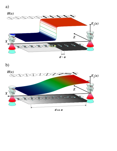
where , and spatially varying magnetic field couples to spin degree of freedom. As it was discussed above, we envision that this magnetic field can be induced by the proximity effect in graphene due to the super-exchange interaction with the magnetic layer contacting the graphene sheet patent ; Haugen_2007 . As a consequence, magnetic field considered in Eq. (4), irrespective of its direction, acts only on spin degree of freedom of quasiparticles in graphene. For the case of spatially homogeneous magnetization of graphene-magnet heterostructure, the spin component directed along the effective field is conserved. Hence, spin-polarized carriers maintain their polarization. Such structure can be used to transport spin-polarized currents. The basic element allowing manipulation of spin-polarized currents in graphene-magnet heterostructures is the region where magnetic field changes its direction, namely the domain wall (DW). In the next section we analyze transmission of the spin-polarized carriers through the domain wall.
IV Passage of spin-polarized Dirac fermions through a domain wall
In order to understand transport properties of an inhomogeneously magnetized graphene heterostructure, we analyze ballistic passage of spin-polarized carrier through the lateral domain wall separating two regions of opposite magnetization, Fig. 2. The transmission through the domain wall is characterized by the amplitudes of spin flip and non-spin-flip processes. These amplitudes determine spin-polarized transport through DW and their knowledge is important for devising spintronics applications of the considered heterostructure.
For definiteness, let us consider electrons in the presence of the magnetic field pointing along and opposite to -axis on different sides of the domain wall located in the stripe region . We further assume it to rotate uniformly within the DW (see Fig. 2). Specifically, we represent the magnetic field with the unit vector
| (5) |
describing its rotation within the DW. In Eq. (5), stands for the unit vector pointing in the -th direction, and the rotation angle is taken to be linear in the lateral coordinate , .
We begin with the qualitative discussion of the carrier passage in the case of normal incidence. Due to the conservation of (pseudo-spin) chirality in the Klein tunneling phenomenon Novoselov_Nature2005 the backscattering is absent in this case. The carrier passes the DW during the passage time , where is the characteristic width of the DW. Within the DW region the spin of the carrier experiences the time dependent torque and undergoes the Larmor precession. The parameter controlling the spin dynamics is the ratio of the passage time to the spin precession period,
| (6) |
For thin DW, , and in the absence of the intervalley scttering, , where is the carrier’s de Broglie wavelength, the spin-flip probability is small, corresponding to a small precession angle. In the opposite limit of thick DW, , the spin follows the varying Zeeman field inside the DW adiabatically and the non-spin-flip probability is small. As a result, the carrier preserves its alignment with the field and reverses its polarization upon passing through the DW. Although the scattering for the arbitrary angle is complicated by the finite backscattering amplitude, the basic physical picture presented above still holds and allows us to construct a scattering theory in the general case.
To solve the scattering problem we construct the scattering state,
| (7) |
where with denotes incoming, reflected and transmitted waves, and the subscript refers to the spin up (down) polarizations, respectively. Due to the translational symmetry in the -direction, the scattering state in Eq. (7) is the eigenstate of the -component of the momentum and can be labeled by its eigenvalue , making our problem effectively one-dimensional. We present wave functions entering Eq. (7) in the following form
| (8) |
Here is the spin wavefunction, i. e. the spinor satisfying , and is a pseudo-spinor in the sublattice space.
Capitalizing on the particle-hole symmetry of the problem, in what follows we only consider the case of incident quasiparticles with . The incoming wave is an eigenstate of the Hamiltonian (4) for . At a fixed energy, the majority (spin down) and minority (spin up) carriers have Fermi momenta and , respectively. Here can be both positive and negative, the latter case corresponds to the hole-like quasiparticles. The kinematic constraint for the incoming spin up (down) electrons reads . Introducing the notation
| (9a) | |||
| (9b) |
for the pseudo-spinor forming angle with -axis, we write the pseudo-spinor of the incoming electron as
| (10c) | ||||
| (10h) | ||||
| where and are step functions distinguishing cases of particle- and hole-like carriers, respectively. In a similar fashion we write for the reflected wave | ||||
| (10m) | ||||
| (10r) | ||||
| The square roots in Eq. (9) are defined as having positive imaginary part for negative argument. This choice, together with the sign and conjugation convention in Eq. (10m), insures that for the wave function of the minority (spin up) carriers decays exponentially away from the DW, namely, it is an evanescent wave. The transmitted waves are given by | ||||
| (10u) | ||||
| (10z) | ||||
Equations (10) when substituted in (8) give the explicit expressions for the incoming, reflected and transmitted spinors in the most general scattering state of Eq. (7).
In order to find the transmission and reflection amplitudes, the transfer matrix matching the wave function at the two boundaries of the DW
| (11) |
has to be found. To this end, we solve the Dirac equation inside the wall,
| (12) |
with the initial condition specifying the wave function at . The equation (12) is formally equivalent to Rabi problem of spin coupled to the oscillating magnetic field Rabi with coordinate playing the role of the time. The field is turned on at the “time” and turned off at “time” . Exploiting this analogy we solve Eq. (12) by the transformation to the rotating reference frame,
| (13) |
such that the field seen by the transformed spin is stationary. Substitution of Eq. (13) into Eq. (12) gives
| (14) |
We notice that static magnetic field now appears effectively as an operator in the pseudo-spin space. We can rewrite Eq. (14) in the form
| (15) |
where . The four-by-four matrix on the right hand side of Eq. (15) reads
| (16) |
with dimensionless energies and and the parameter defined in Eq. (6). The formal solution of equation (15) is
| (17) |
Combining equations (11), (13) and (17) we obtain
| (18) |
The exponentiation in Eq. (18) can be performed explicitly as follows
| (19) |
where notations
| (20) | ||||
have been introduced, and
| (21) |
are projection operators onto the subspaces of the eigenvalues of the matrix
| (22) |
Equations (18), (19), (21), and (22) give the transfer matrix introduced in equation (11) as a third degree polynomial in matrix . For an arbitrary angle of incidence the transmission and reflection coefficients are found by imposing the matching condition in Eq. (11) on the scattering state of Eq. (7). The resulting system of four linear equations determining four coefficients , can be easily solved. For the incoming (spin up) minority carriers the probabilities of the passage with and without spin flip are given by
| (23) |
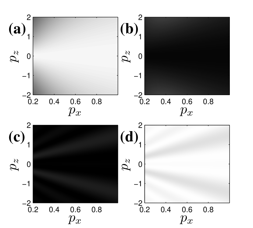
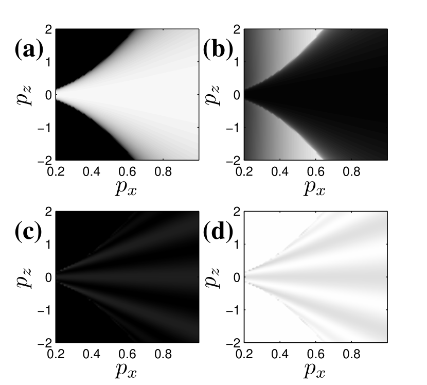
Although the solution of linear matching equations is straightforward, the final expressions are somewhat cumbersome and below we present the results graphically. The transmission probabilities for the incoming minority (spin up) and majority (spin down) species, respectively, are shown in Figs. 3 and 4. In both figures, panels (b) and (d) present the transmission with the spin flip, and panels (a) and (c) the transmission without the spin flip. Panels in the upper row show the case of the thin DW, , and panels in the lower row the case of the thick DW, .
Unlike the case of the normal incidence, for the incidence at an arbitrary angle the chirality is not conserved, leading to a finite backscattering probability. Hence, particles passing the DW experience spin-dependent reflection and refraction. The Snell’s law relating the angles of propagation of the incoming and the outgoing particles to the refraction indices of the two media reads
| (24) |
The conservation of the -component of the momentum gives for the ratio of the refractive indexes,
| (25) |
The behavior of this ratio for two spin polarizations as a function of energy is shown in Fig. 5.
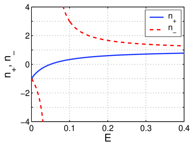
It follows from Eq. (25) that the DW has a different effect on the spin minority and the spin majority carriers. The minority carriers passing the DW experience the increase of the optical density, while the majority carriers experience the decrease of it. An interesting regime occurs when the energy of incoming particles . In this case the ratio in Eq. (25) becomes negative and results in the spin dependent Veselago lens effect, similar to that discussed in Ref. Cheianov-Science2008, .
The above spin-optics arguments are useful in understanding the results shown in Figs. 3 and 4. For the incidence at a shallow angle the probability of non-spin-flip passage is suppressed as particle trajectory even in the narrow DW becomes long. The difference between the incoming minority and majority species in Figs. 3(a,b) and 4(a,b) results from the different refraction coefficients for the two species imposed by the kinematical constraints. The refraction coefficient ratio for minority carriers is , and their trajectories bend so that the path inside the DW shortens. For the majority carriers, on the other hand, , and the trajectory bending leads to the longer path inside the DW. Therefore, the effect of magnetic field inside the DW and the probability of transition without the spin flip are enhanced for the minority carriers, Fig. 3(a), and suppressed for the majority carriers, Fig. 4(a).
The Fabry-Pérot pattern of transmission seen in Figs. 3(d) and 4(d) is a consequence of an interference of multiple reflections inside the thick DW.
IV.1 Normal Incidence
Our results are substantially simplified in the case of normal incidence, when the momentum component vanishes. With the equation (19) reduces to
| (26) |
The last equation gives for the transfer matrix
| (27) |
where the overall phase factor has been omitted. In the present section we focus on the transmission probabilities. It has to be stressed however that the phase of the transition amplitude is also of interest, especially if the magnetization vector completes one or more rotation circles inside the DW. Under the conditions of adiabatic spin transfer, this phase is geometric Berry1984 , see the discussion of geometric Berry phase for the DW passage in App. A.
In the case of normal incidence the chirality is a good quantum number, . This ensures the absence of backscattering (Klein tunneling phenomenon). For the incoming particles with we have . Therefore, dynamics in the case of normal incidence occurs in the spin sector only. The particle traveling inside the DW experiences the action of magnetic field rotating with the frequency . The probability of passing the DW without the spin flip is given by the diagonal element of the transfer matrix
| (28) |
Here, is the rotation angle accumulated by the spin precessing at the Rabi frequency, , during the passage time . It follows from Eq. (28) that the polarization of the impinging particle is not influenced by the DW in the case of the thin wall, . In the opposite limit of the thick DW, , electron spin adjusts adiabatically following the direction of the magnetic field slowly varying inside the DW.
Our results for the case of normal incidence are in agreement with Ref. Newton1948, , where neutron polarization change in the course of the passage through the ferromagnetic domain wall is analyzed. We note that in the non-relativistic case Newton1948 the absence of backscattering is an approximation, which is valid for neutrons with high enough energy. This approximation fails for low energy particles, as inside the DW particles experience a force which results from the magnetic field gradient inside the DW. In the present, relativistic, case however the carriers with arbitrarily low energy can not be reflected by the DW because of the chirality conservation. Therefore, in the relativistic case the thick domain wall is efficient in flipping spins of particles incident at .
Until now we have discussed the case of the DW with well-defined, abrupt boundaries, where the region of magnetic field variation is limited to a finite interval [see Eq. (5)]. While in most cases this is a reasonable description (in particular, for patterned structures), in some experimental realizations of spintronic devices the boundaries of the DW may be smooth and not well defined. To clarify the significance of the above distinction in the DW structure we consider the DW with the magnetic field direction with the angle following the Rosen-Zener profile, . In this case the non-spin-flip transmission amplitude can be found exactly RosenZener ,
| (29) |
It follows from comparison of Eq. (28) and Eq. (29) that the DW with smooth boundaries polarizes the incoming carriers even more efficiently than the DW with abrupt boundaries. Hence, we argue that both for thin DW, , and thick DW, , cases our conclusions are valid for the DW of an arbitrary shape.
V Conductance in the ballistic transport regime
In the high quality graphene devices the mean free path is comparable to the characteristic sample size. Under such conditions the transport through DW structures is ballistic. The conductance can be obtained within the Landauer approach. In spintronic devices we consider the spin selective transport, as they manipulate the currents of the electrons of different polarizations independently. Two terminal conductance is given by the sum of the transmission probabilities over all active conductance channels. Both majority and minority spin channels give rise to currents of carriers of both polarizations. We introduce the spin dependent conductance to denote the contribution of incoming carriers with spin in the source channels to the current of carriers with spin in the drain channels,
| (30) |
where we have taken into account the 2-fold valley degeneracy. The above definition is meaningful due to the conservation of -component of spin away from the DW.
Partial conductances obtained from Eq. (30) are plotted in Fig. 6 as a function of the chemical potential for two thicknesses of the DW, , (a,c) and , (b,d).
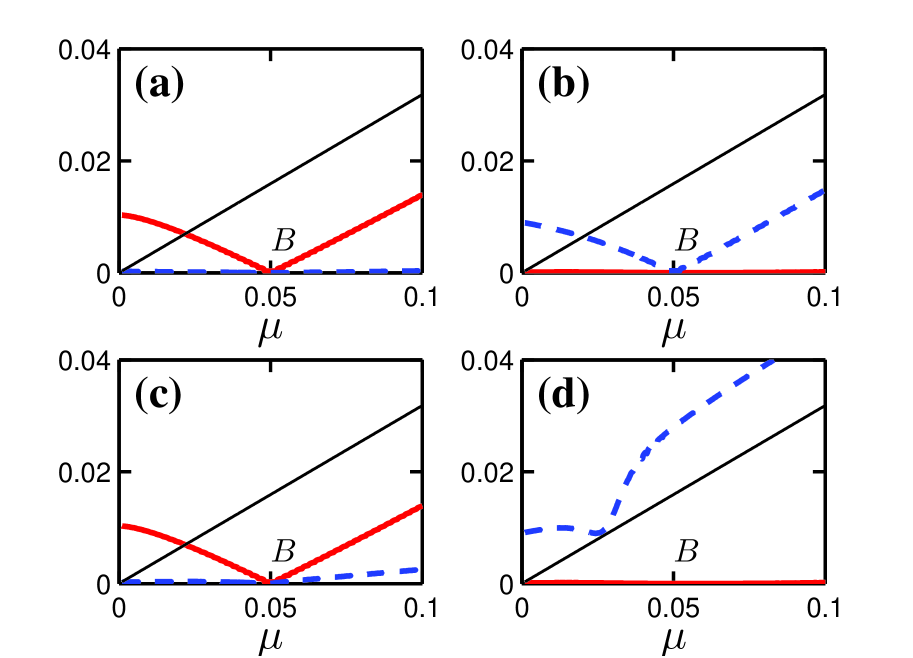
The partial conductance for the positive spin polarization in the source, , is shown in the upper row, Fig. 6(a,b). That for is shown in the bottom row, Fig. 6(c,d). Solid lines corresponds to the spin flip processes, namely and dashed lines represent the diagonal conductances with .
The common feature of the curves shown in Fig. 6 is the conductance growth when the chemical potential exceeds half of the spin splitting, . This is clearly due to the increase of the number of conducting channels. Secondly, the increased thickness of the DW stimulates spin flip processes. This is a consequence of the adiabatic transfer of the spin inside the thick DW discussed in Sec. IV. In addition, the only conductance not vanishing at the special point in the case of the thick DW is , see Fig. 6(d), dashed line. This is easily understood from the following consideration. For the thin DW the spin is approximately conserved. For that reason, the spin minority (majority) carriers have vanishingly small number of incoming (outgoing) channels at , leading to a small conductance. In the case of the thick DW the spin majority carrier can remain spin majority carrier by adiabatically adjusting (reversing) its spin polarization. This yields finite conductance at . The specifics of the point described above makes hetero-structures with the Dirac spectrum of quasi-particles promising candidates for spin manipulation of the currents in spintronics.
VI Summary and Discussion
In the present paper we have analyzed the passage of spin-polarized Dirac charge carriers through the DW in graphene-magnet hetero-structure. We have calculated the transmission and the reflection probabilities as a function of the energy of the incoming particles, which is determined by the average chemical potential in the graphene sample, for the DW of different thickness. The knowledge of the transmission amplitudes has allowed us to calculate the conductances of different spin channels in two-terminal geometry. The spin-polarized transport depends crucially on the thickness of the DW. Below we discuss the main features of our results and their potential applications in graphene-based spintronic elements.
We have considered two limiting cases of thin and thick DW. In the case of thin DW the spin dynamics inside the DW only occurs for shallow incidence angles. Aside from this special case, the spin is approximately conserved and the transmission is governed entirely by the kinematics of the relativistic Dirac quasiparticles in graphene, establishing direct connection with the problem of Klein tunneling and chiral dynamics in 2D quantum electrodymanics. A similar problem has recently been considered in the context of junctions in graphene devices Cheianov-Science2008 ; Katsnelson_NatMat2006 ; Katsnelson_SSC2007 . In our case the DW presents a junction for the majority and a junction for the minority carriers. The non-spin-flip transmission for is allowed through the particle-hole transmutation – the Klein tunneling phenomenon.
The transmission properties of the thin DW can be nicely understood in the context of spin-optics Khodas2007 . As it follows from the ratios of the refraction indices in Fig. 5, the trajectories of the minority (spin up) carriers bend inward, while those of the majority carriers bend outward. This difference is most pronounced near , where the refraction index changes in sign, becoming negative for both spin polarizations at . Near this point the transmission of the majority carriers through narrow DW vanishes and the corresponding refraction index diverges. The index of refraction for the minority carriers, on the other hand, is close to 0, as they can only pass through the DW near the forward direction. Hence, there is a giant birefringence of carriers with different spin polarizations, which could be employed in spin-selective transport devices. At , the spin majority carriers undergo the total internal reflection due to the kinematic constraint, which occurs in a wide angular interval corresponding to dark areas in Fig. 4(a). In the regime close to the total reflection the length of the particle’s trajectory even inside a narrow DW becomes increasingly large. Hence, the probability of the spin-flip transmission becomes significant, see Fig. 4(b). In this regime the angular aperture of the spin minority carriers becomes small, and thin DW is an efficient spin polarizer.
In the case of the thick DW the passage is governed by the spin dynamics inside the domain wall and the conductance is controlled by the adiabatic nature of the spin transport. Independent of their energy, both majority and minority carriers simply flip their spins, remaining in their respective channels, so that thick DW acts as a spin-flipper for spin-polarized currents. As in the case of the thin DW considered above, the effect of the DW on the transport is most pronounced when the chemical potential is tuned to near the spin splitting, . In this case the Fermi surface of the minority spin carriers in the region shrinks to a point and the current is carried by the majority species. In contrast to the case of the thin DW, the majority carriers in the region are transformed to the majority carriers in the region by adiabatically adjusting their spin. This gives finite conductance for , which is off-diagonal in spin, see Fig. 6(d). Thus, a spin-transistor action could be achieved by virtue of adjusting the chemical potential in a gated device with magnetic layer coupled to the graphene layer.
Finally, manipulating the spin polarization of electrons in graphene by the means of Zeeman band splitting such as discussed in this paper depends crucially on the strength of the polarizing magnetic field. In the case of the passage through a DW, this strength also determines the relevant physical thickness distinguishing the cases of thick and thin DW, Eq. (6). In the case of the laboratory magnetic field of created by a solenoid, the Zeeman band splitting is meV. The condition requires extremely thick DW, m. Moreover, such field results in a negligible spin-splitting, which corresponds to a temperature of only K, and negligible charge carrier density, cm-2, Eq (3).
However in the case of a spin-dependent band splitting induced by the magnetic proximity effect in graphene-magnet hetero-structure the corresponding effective spin-polarizing field could be expected to be of the order of hundreds, or even a thousand Kelvins. Physically, it could be estimated from the characteristic ordering temperature of the magnetic layer, and corresponds to 10 meV to 100 meV spin-dependent band splitting. Then, the effective “exchange” field could be as large as T, resulting in cm-2 and nm.
Is it reasonable to expect such large magnetic proximity effects in graphene-magnet heterostructures? Theoretical estimates for the graphene layer in contact with EuO, one of the few insulating Heisenberg ferromagnets, predict band splitting of meV Haugen_2007 . This agrees well with the Curie temperature K for this material. For room-temperature magnetic materials, the splitting could be expected to be proportionally higher. For example, one can envision using NiO [111] film in contact with graphene. NiO is an antiferromagnet with the Neel temperature K, where ferromagnetically aligned Ni layers alternate in the [111] direction. In the artificial [111] nano-layer CoO/NiO and NiO/Fe3O4 superlattices the proximity effect-induced increases of the ordering temperature by hundreds of Kelvins have been observed BorchersErwin_PRL1993 . It does not seem unreasonable to extrapolate this effect to graphene-magnet heterostructures. Finally, the technology of manufacturing graphene-based heterostructures is developing quite rapidly. The growth of the atomically smooth epitaxial MgO film on graphene has recently been reported Wang_APL2008 , as were nonvolatile memory devices obtained by covering graphene with a ferroelectric layer Ozyilmaz . Therefore, manufacturing graphene-magnet heterostructures in order to achieve manipulation with spin-polarized currents such as considered in this paper looks reasonable and promising approach to be attempted experimentally.
In closing, we would like to note an interesting analogy between the generation of spin-polarized electric current in graphene hetero-structures and the separation of electric charge of quarks in strong external magnetic fields in the presence of the topological charge in the quark-gluon plasma produced in relativistic heavy ion collisions Kharzeev:2004ey . There is a recent evidenceVoloshin:2008jx for this effect from STAR Collaboration at RHIC (BNL).
Acknowledgements.
Illuminating discussions with A. Tsvelik, T. Valla and Y. Bazaliy are greatly appreciated. This work was supported under the Contract No. DE-AC02-98CH10886 with the U. S. Department of Energy. M. K. acknowledges support from the BNL LDRD Grant No. 08-002.Appendix A Geometrical phase of carriers passing the DW
The purpose of this appendix is to illustrate the general concept of geometrical phases Berry1984 for the spin carriers passing the DW described by the Hamiltonian of Eq. (4). We consider the normal incidence case where the dynamics occurs in spin sector only. Here we are interested in the limit of adiabatic spin transfer realized in sufficiently thick DW. The direction of the magnetic field is a parameter of the system changing slowly inside the DW,
| (31) |
where , and
| (32) |
In the last equation we assume . For , the magnetic field defined by Eqs. (31) and (32) acting on a particle passing the DW completes a circle, sweeping the conical surface in -space. It is identical for and . Therefore, the wave function adiabatically following the instantaneous eigenstate can only acquire the phase factor after the DW passage,
| (33) |
The first factor represents the dynamical phase due to the spin precession in magnetic field, and the second factor is geometric Berry phase, independent of the DW structure in the adiabatic limit. Below we calculate the geometrical phase explicitly for the specific model of DW specified by Eqs. (31) and (32), and compare it with the known theoretical results.
We calculate transmission amplitudes for two spinors which are exact eigenstates of the Hamiltonian for . The spin in these states is polarized parallel (anti-parallel) to the magnetic field outside the DW, i.e.
| (34) |
In the last equation we use the notation
| (35) |
similar to Eq. (6). The transmission amplitudes are diagonal elements of the inverse transfer matrix defined in Eq. (11),
| (36) |
The unitary transfer matrix is found following the same approach as in Sec. IV
| (37) |
Substituting Eqs. (A) and (34) in Eq. (36) we obtain
| (38) |
where we made an expansion
| (39) |
valid in the adiabatic limit, . Comparing Eq. (A) with Eq. (33) we identify the first factor as corresponding to the dynamical phase
due to the orbital motion and precession in the magnetic field, and the second factor as the geometrical Berry phase,
| (41) |
where is an opening angle of the cone swept by the magnetic field in the DW. Equivalently, the phase is half of the solid angle subtended by the closed contour in the -space at the degeneracy point , in agreement with the general theory. We notice that the geometrical phase is of opposite sign for two spin orientations . The resulting deviation of the precession angle from the one expected from Eq. (A) has been observed experimentally for neutrons passing the region of the spiral magnetic field NeutronsBook . We argue that similar phenomenon could be observed in graphene samples for carriers passing the DW with the magnetic field rotation angle, .
References
- (1) A. K. Geim, K. S. Novoselov, Nature Mater. 6, 183 (2007).
- (2) L. D. Landau, E. M. Lifshitz, Statistical Physics, Part I (Pergamon Press, Oxford, 1980).
- (3) C. Oshima and A. Nagashima, J. Phys.: Condens. Matter 9, 1-20 (1997).
- (4) I. Forbeaux, J.-M. Themlin, J.-M. Debever, Phys. Rev. B 58, 16396 (1998).
- (5) K. S. Novoselov, D. Jiang, F. Schedin, T. J. Booth, V. V. Khotkevich, S. V. Morozov, K. A. Geim, Proc. Natl. Acad. Sci. USA 102, 10451 (2005).
- (6) A. Charrier, A. Coati, T. Argunova, F. Thibaudau, Y. Garreau, R. Pinchaux, I. Forbeaux, J.-M. Debever, M. Sauvage-Simkin, J.-M. Tremlin, J. Appl. Phys. 92, 2749-2484 (2002).
- (7) T. Ohta, A. Bostwick, J. L. McChesney, T. Seyller, K. Horn, E. Rotenberg, Phys. Rev. Lett. 98 206802-1, (2007).
- (8) K. S. Novoselov, A. K. Geim, S. V. Morozov, D. Jiang, Y. Zhang, S. V. Dubonos, I. V. Grigorieva, and A. A. Firsov, Science 22 (2004).
- (9) C. Berger, Z. Song, X. Li, X. Wu, N. Brown, C. Naud, D. Mayou, T. Li, J. Hass, A. N. Marchenkov, E. H. Conrad, P. N. First, W. A. de Heer, Science 312, 1191-1196 (2006).
- (10) J. Hass, R. Feng, T. Li, Z. Zong, W. A. deHeer, P. N. First, E. H. Conrad, C. A. Jeffrey, C. Berger, Appl. Phys. Lett. 89, 143106 (2006).
- (11) D. C. Tsui, H. L. Stormer, and A. C. Gossard, Phys. Rev. Lett. 48, 1559 (1982).
- (12) K. S. Novoselov, A. K. Geim, S. V. Morozov, D. Jiang, M. I. Katsnelson, I. V. Grigorieva, S. V. Dubonos and A. A. Firsov, Nature 438, 197-200 (2005).
- (13) Y. Zhang, Y. W. Tan, H. L. Stormer and P. Kim, Nature 438, 201-204 (2005).
- (14) K. S. Novoselov, Z. Jiang, Y. Zhang, S. V. Morozov, H. L. Stormer, U. Zeitler, J. C. Maan, G. S. Boebinger, P. Kim, and A. K. Geim, Science 315, 1379 (2007).
- (15) D. V. Khveshchenko, Phys. Rev. Lett. 87, 246802 (2001); ibid. 87, 206401 (2001); D. V. Khveshchenko and H. Leal, Nucl. Phys. B687, 323 (2004); D. V. Khveshchenko and W. F. Shively, Phys. Rev. B73, 115104 (2006).
- (16) E. V. Gorbar, V. P. Gusynin, V. A. Miransky and I. A. Shovkovy, Phys. Rev. B66, 045108 (2002).
- (17) A. De Martino, L. Dell Anna, and R. Egger, Phys. Rev. Lett. 98, 066802 (2007).
- (18) I. L. Aleiner, D. E. Kharzeev, and A. M. Tsvelik, Phys. Rev. B 76, 195415 (2007).
- (19) N. Tombros, C. Josza, M. Popinciuc, H. Jonkman, B. J. van Wees, Nature 448, 571 (2007).
- (20) S. Cho, Y. Chen, M. Fuhrer, Appl. Phys. Lett. 91, 123105 (2007).
- (21) E. W. Hill, A. K. Geim, K. Novoselov, F. Schedin, P. Blake, IEEE Trans. Magn. 42, 2694-2696 (2006).
- (22) I. A. Zaliznyak, A. M. Tsvelik, D. E. Kharzeev, US provisional patent application # 60/892,595 (2006).
- (23) H. Haugen, D. Huertas-Hernando, A. Brataas, Phys. Rev. B 77, 115406 (2008).
- (24) A. D. Kent, J. Yu, U. Rüdinger, S. S. Parkin, J. Phys.: Condens. Matter 13, R461 (2001).
- (25) I. I. Rabi, Phys. Rev. 51, 652 (1937).
- (26) V. V. Cheianov, V. Fal’ko, and B. L. Altshuler, Science 315, 1252 (2007).
- (27) M. V. Berry, Proc. Royal Soc. of London, A392, 45 (1984).
- (28) R. R. Newton, and C. Kittel, Phys. Rev. 74, 1604 (1948).
- (29) N. Rosen, and C. Zener, Phys. Rev. 40, 502 (1932).
- (30) T. Matsuyama, C.-M. Hu, D. Grundler, G. Meier, and U. Merkt, Phys. Rev. B 65, 155322 (2002)
- (31) M. I. Katsnelson, K. S. Novoselov and A. K. Geim, Nature Materials 2, 620 (2006).
- (32) M. I. Katsnelson, K. S. Novoselov, Sol. St. Comm. 143, 3 (2007), and references therein.
- (33) M. Khodas, A. Shekhter, and A. M. Finkeĺstein, Phys. Rev. Lett. 92, 086602 (2004).
- (34) J. A. Borchers, M. J. Carey, R. W. Erwin, C. F. Majkrzak, A. E. Berkowitz, Phys. Rev. Lett. 70, 1878-1881 (1993); J. A. Borchers, R. W. Erwin, S. D. Berry, D. M. Lind, J. F. Alkner, E. Lochner, K. A. Shaw, D. Hilton, Phys. Rev. B 51, 8276-8286 (1995).
- (35) W. H. Wang, W. Han, K. Pi, K. M. McCreary, F. Miao, W. Bao, C. N. Lau, R. K. Kawakami, Appl. Phys. Lett. 93, 183107 (2008).
- (36) B. Özymilaz, et. al., Technology Review (MIT press), http://www.technologyreview.com (unpublished).
- (37) D. Kharzeev, Phys. Lett. B 633, 260 (2006) [arXiv:hep-ph/0406125]; D. Kharzeev and A. Zhitnitsky, Nucl. Phys. A 797, 67 (2007) [arXiv:0706.1026 [hep-ph]]; D. E. Kharzeev, L. D. McLerran and H. J. Warringa, Nucl. Phys. A 803, 227 (2008) [arXiv:0711.0950 [hep-ph]]; K. Fukushima, D. E. Kharzeev and H. J. Warringa, Phys. Rev. D 78, 074033 (2008) [arXiv:0808.3382 [hep-ph]].
- (38) S. A. Voloshin [STAR Collaboration], arXiv:0806.0029 [nucl-ex]; and talk at Quark Matter 2009 Conference, Knoxville, TN.
- (39) H. Rauch, S. A. Werner, Neutron Interferometry: Lessons in Experimental Quantum Mechanics, Oxford University Press, USA (2000).