Characterisation of Ferromagnetic Contacts to Carbon Nanotubes
Abstract
We present an investigation of different thin-film evaporated ferromagnetic materials for their suitability as electrodes in individual single-wall and multi-wall carbon nanotube-based spin devices. Various electrode shapes made from permalloy (), the diluted ferromagnet , and bilayers are studied for both their micromagnetic properties and their contact formation to carbon nanotubes. Suitable devices are tested in low-temperature electron transport measurements, displaying the typical tunneling magnetoresistance of carbon nanotube pseudo spin valves.
pacs:
75.75.+a, 75.70.Kw, 85.35.Kt, 72.25.-bI Introduction
Carbon nanotubes have been a widely investigated material for spintronics devices over the last years, which is above all due to their unique electrical properties, i. e. high Fermi velocity, quasi one-dimensional ballistic transport, long spin lifetimes, and weak influence of nuclear spin.Prinz (1998); Cottet et al. (2006) To obtain spin-dependent electron emission or absorption, a nanotube is typically contacted by ferromagnetic electrodes. Thin-film ferromagnets diluted with Pd are known to make a good electrical contact to individual carbon nanotubes, accessing the KondoHauptmann et al. (2008); Buitelaar et al. (2002) and Fabry-Perot regimes.Man et al. (2006) Pd is used for its contact transparency to carbon nanotubesJavey et al. (2003a) and its transgression into a ferromagnetic phase with even small admixture of a ferromagnet.Stirling et al. (1972) For both multiwallSahoo et al. (2005a); Buitelaar et al. (2002); Cottet et al. (2006); Zhao et al. (2002) and single wall carbon nanotube devices,Sahoo et al. (2005b); Man et al. (2006); Hauptmann et al. (2008); Cottet et al. (2006) the tunnel magnetoresistance (TMR)Julliere (1975) has been observed. Any industrial application of the observed principles, however, will require a large degree of reproducibility and control, in particular regarding the detailed micromagnetic structure of the nanotube contact electrodes.
This work aims at an improvement of the switching properties of the ferromagnetic electrodes, i. e. obtaining reliable reversal of the magnetisation at reproducible coercive field values, with a focus on PdFe alloys. Simultaneously, we monitor the electrical interface quality from ferromagnet to nanotube, including low-temperature magnetotransport measurements. Here, reliable control of magnetic switching is of particular importance as there are no direct means to check the magnetic domain structure once the sample is mounted in a cryostat for transport measurements.
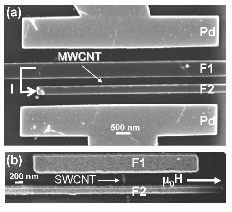
We investigate a typical pseudo spin valve geometry,Sahoo et al. (2005a); Kim et al. (2002); Zhao et al. (2002); Man et al. (2006) as shown in Fig. 1(a) for a multi-wall carbon nanotube (MWCNT) and in (b) for a single-wall carbon nanotube (SWCNT). Two ferromagnetic electrodes F1 and F2 are designed such that they have a different coercive field. This is achieved here by making use of shape anisotropy, which can be tuned via the sample geometry. In magnetoresistance measurements, a sufficiently large external magnetic field is applied to saturate and align the magnetisation of both contacts in parallel to it. A magnetic field sweep to opposite field direction will first switch the magnetisation of the contact with smaller coercive field, thereby achieving antiparallel configuration, and then the magnetisation of the second, resulting in a parallel configuration with polarity opposite to the initial one.
II Lorentz microscopy imaging of the magnetic switching of ferromagnetic electrodes
For carbon nanotube magnetotransport experiments, the ferromagnetic contact electrodes are required to have a difference in coercive field large enough to be resolvable in transport measurements, e.g. or more. A second requirement for reliable and reproducible magnetic switching is that the segment of the electrode contacting the carbon nanotube be in a well-defined single domain state to allow experimental control over injecting a spin-polarized current. Transmission electron microscopy (TEM) in Lorentz microscopy mode provides a powerful tool to investigate these properties of thin ferromagnetic films.
II.1 Methods
Lorentz microscopyChapman (1999); Lim (2002); Uhlig and Zweck (2004) allows direct observation of the magnetic domain structure of a ferromagnetic structure and its evolution in an external magnetic field by sending a parallel (out of focus) electron beam through a magnetic specimen. The deflection of the beam due to the Lorentz force can be visualized by defocusing the objective lens. At the walls enclosing a magnetic domain, the electrons are deflected as they transverse the ferromagnetic film and form either a convergent or a divergent set of partial electron waves. Correspondingly, an increase or a decrease of the electron beam intensity is detected at the location of domain walls. It should be noted that not only domain walls but also other variations in the magnetic induction within the specimen can be visualized by this technique.
If the specimen is magnetized homogeneously, every transmitted electron will be deflected to the same side. In this case, a brightly contrasted feature forms on the edge of the specimen where the deflected beam through it overlaps with the undeflected beam passing next to it. On the opposite side, the deflection of the electrons will partially deplete the edge region which manifests in a dark contrast line on the detector.
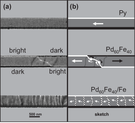
These dark and bright contrast features can, for instance, be seen within the permalloy strip shown in the topmost panel of Fig. 2. Magnetic domain walls, where spins oppose each other in frustration, appear as dark or bright features within the strip area (see middle panel of Fig. 2). A detailed discussion of Fig. 2 will be given below.
Driving the electron beam focus from above to below the sample plane reverses the Lorentz-force induced contrast, providing a consistency test as to whether observed features are indeed of magnetic origin. A magnetisation reversal due to an external magnetic field can be detected by observing subsequent images during a field sweep when a structure’s edge contrast is inverted. Note that on the borders of the observed ferromagnetic structures, the dark Lorentz contrast appears more pronounced than the bright one. This is partly owed to a superposition with a bright contrast all around the observed structures stemming from Fresnel edge diffraction. The magnetisation structure can therefore be read off most clearly by tracing structures of dark edge contrast.
In the TEM used for the work at hand, an external magnetic field can be applied only in parallel to the electron beam, i. e. perpendicular to the sample plane. An in-plane field component with respect to the sample plane can be tuned by maintaining this field at constant magnitude and tilting the sample by an angle . At a maximum tilt angle of , the in-plane component reaches about half the value of the out-of-plane component. Rotating the sample and thereby sweeping the in-plane field from saturation through zero field to saturation in opposite direction allows to monitor the magnetisation reversal process of the ferromagnetic specimen.
Electron transmission microscopy requires samples to be prepared on a grid or thin film membrane with low electron beam contrast. The metal test structures were patterned by electron beam lithography (EBL) and thermally evaporated in vacuum onto thin low-stress PECVD silicon nitride membranes. Owing to shape anisotropy, Néel walls, i. e. with the frustrated spins being confined to the film plane, occur in sufficiently thin ferromagnetic films. Above a material-specific thickness, which is smaller for weaker magnetisation, Bloch walls dominate. Here, the spins form domain walls by gradually turning out of the film plane. According to our experience, the threshold thickness of permalloy (Py, ) films is about . We therefore keep the film thicknesses below that value. Also the large aspect ratio of film thickness compared to the lateral electrode dimensions is expected to favour an in-plane orientation of the magnetisation.Hubert and Schäfer (1998) We hence start our discussion with the effect of this in-plane magnetic field component. In any case, effects of magnetisation and magnetic field components parallel to the electron beam are not imaged in Lorentz microscopy, due to the cross product in the Lorentz force.
II.2 Material dependence of the domain structure and magnetisation reversal properties
The investigated materials are chosen for their magnetic properties or expected contact transparency to carbon nanotubes. We consider Permalloy (Py, ) and the giant paramagnet Pd diluted with Fe, as we expect diluted ferromagnetic PdFe alloys to combine the benefits of the strong ferromagnetism of iron and the transparent contacts of palladium – carbon nanotube interfaces.Javey et al. (2003a); Cottet et al. (2006) The composition of the PdFe alloy is adjusted by setting the evaporation rates from two confocal thermal evaporation sources appropriately. In addition, magnetic bilayer structures with of and a -thick Fe layer – to stabilize the magnetisation of the magnetically soft PdFe by the magnetically hard Fe – are discussed. To prevent the iron from oxidation and for improved interface resistance with the Pd leads, these bilayers were additionally capped with of Pd.
In Fig. 2(a), rectangular strips of equal dimensions made from these three polycrystalline materials are compared. To allow comparison of the domain structure in different ferromagnets, the Lorentz microscopy images are taken at the field values close to magnetisation reversal in the specific material. We concentrate initially on the central segment of the strip, where the contacted carbon nanotube would be placed in transport measurements. The majority spin orientation and magnetic domain structure of this portion determines spin orientation and polarisation of an injected current. The sketches of Fig. 2(b) point out the relevant magnetic features of the Lorentz images.
II.2.1 Permalloy
Permalloy (Py) was a chosen as a ferromagnetic material for its high magnetic permeability, low coercive field, and large magnetic anisotropy.Hubert and Schäfer (1998); Gomez et al. (1999); Shalyguina et al. (2002) From the homogeneity of the entire Py strip in Fig. 2(a) it can be concluded that the observed segment is in a single domain state. In the Lorentz image the magnetic domain appears bordered by a continuous bright contrast line on the top side and a dark one on the bottom side. The corresponding arrow in Fig. 2(b) symbolizes this uniform magnetisation orientation of the single domain. Note that the absolute direction of the magnetisation can only be determined from the dynamics during a full magnetic sweep by comparing subsequent Lorentz images.
II.2.2 PdFe alloy
In contrast to Py, the strip segment in Fig. 2(a) is in a two-domain state at a small field increase beyond magnetisation reversal but not yet saturated. The black and white arrows in the sketch of Fig. 2(b) highlight the opposite magnetisation orientation of the domains. The border contrast changes from bright to dark where the sharp white line connects to the strip boundary. In addition, three dark-contrasted, roughly parallel lines can be made out crossing the bright line. Such so-called cross-tie wall structures are typical for samples between Néel and Bloch phaseHubert and Schäfer (1998) where a successive row of in-plane (Néel) and out-of-plane (Bloch) type walls occurs. For our polycrystalline specimen, we expect a vanishing crystalline anisotropy, so the magnetic dipolar(or shape) anisotropy is dominant. Due to the small magnetisation of compared to stronger ferromagnetic materials, also the shape anisotropy is small. This means that even low magnetic fields perpendicular to the film can lead to relatively large normal components of magnetisation. In any case, magnetic multi-domain and cross-tie wall configurations of the strip render its magnetisation configuration ill-defined for the operation of a CNT pseudo spin-valve. Furthermore, the specific domain wall pattern is often different for any two magnetic sweeps. Occurrence of magnetoresistance in a pseudo spin valve fabricated from this material is therefore prone to a random domain configuration and the position of magnetic pinning centers.
II.2.3 PdFe alloy with a Fe magnetisation stabilisation layer
The bilayer strips display a more uniform overall magnetisation, as indicated by a continuous dark, respectively bright, contrast along the entire borderlines of the strip. In addition, a fine structure appears in Fig. 2(a), which signals the presence of ripple domains, i.e. areas in which the spins deviate from the overall magnetisation direction by a small angle as sketched in the bottom structure of Fig. 2(b). The formation of ripple domains is a well-known phenomenon for thin film materials with a high saturation magnetisation like Fe,Hubert and Schäfer (1998) suggesting that the Fe layer dominates the magnetic properties of the strip.
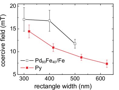
Fig. 3 compares the switching behaviour of and strips of equal lateral dimension and total thickness of . While the magnetic bilayer switches at higher fields than permalloy, it does so with a much higher margin of error.
II.3 Shape dependence of the coercive field
Next, we compare the magnetic switching behaviour of rectangular, needle-shapedYu et al. (1999); Kirk et al. (1999) and spoon-shapedHuber (2005) electrode structures in order to identify the optimal geometry parameters for magnetic switching reproducibility and controllability. It is well-known that by choice of very high aspect ratio of length to width, the smaller of the two parameters dominates the switching behaviour via shape anisotropy. By setting the length to for all structures, investigations can be reduced to varying the electrode widths in the range from up to . Lorentz microscopy allows to determine whether a structures is of suitable dimensions to be in a single domain configuration.
II.3.1 Rectangles
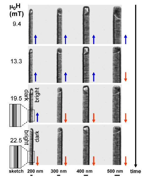
Fig. 4 shows four contact strips of different width at different values of the external magnetic field . Coming from saturation, where all strip magnetisations are aligned along (blue arrows, top image row), the external field is swept to opposite field direction . As indicated by the arrow on the edge, subsequent image rows are recorded at increasing field values during a magnetic field sweep. The images show that the rectangular strips flip their magnetisation consecutively at coercive fields increasing in order of decreasing strip width.
An interesting feature visible in Fig. 4 is the formation of a magnetic end domain at the upper end of the electrode. Its evolution can be monitored by following the magnetic features at increasing field values. It indicates that the magnetic end domains nucleate the magnetic switching of the whole strip. Otherwise, the strips all show a clear single magnetisation direction as desired for a pseudo spin valve contact electrode.
II.3.2 Needle-shaped structures
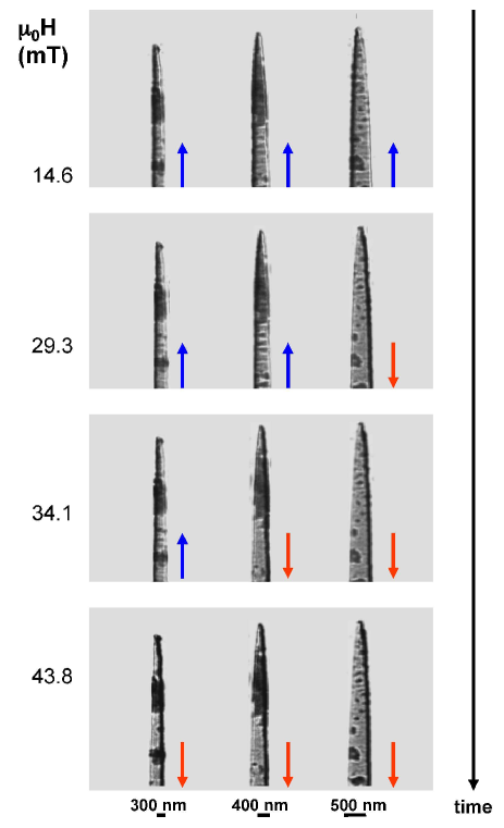
In Fig. 5, three needle-shaped structures of different width are Lorentz-imaged. A magnetisation reversal analogous to Fig. 4 is found. Compared to rectangles, switching in needles is also governed by the structure width but occurs at higher coercive field. This may be explained by fewer magnetically frustrated spins within the pointed structure tips, i. e. fewer and smaller end domains, see Fig. 5 compared to the rectangles of Fig. 4. As the magnetisation reversal is initiated by these end domains, their suppression also should translate into higher magnetisation stability.
II.3.3 Spoon-shaped structures
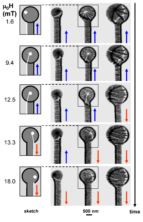
In Fig. 6, TEM Lorentz microscopy images of spoon-shaped structures, i. e. rectangular strips with attached disk, are presented. The disk diameter dependence of the magnetisation reversal of attached rectangular strips is investigated. All strips have equal dimension, only the disk diameters are varied.
In a disk made from a ferromagnetic material, the spins can align in a vortex configuration.Hubert and Schäfer (1998) Depending on whether the vortex chirality is clockwise or counter-clockwise, the vortex core appears in the Lorentz image as either a dark spot (structure in the first column of Fig. 6) or as a bright spot (second column). At zero external magnetic field, the vortex core is near the center of the disk. An external magnetic field along the strip “shoves” the bright (dark) vortex core to the right-hand side (left-hand side).
This behaviour can be observed most clearly in the example of the second column of Fig. 6, where the magnetisation reversal of a “spoon” with a diameter disc is shown. A domain wall, seen as a bright line in the images, originates from the vortex core for all magnetic field values. Sweeping up from negative values of , the vortex core is still shifted at to the left-hand side, owing to the magnetic remanence of the structure. The domain wall ends at the left-hand side of the disk. A field of is required to counter the magnetic remanence so the vortex is moved to the disk center. The white domain wall ends now near the joining of disk and strip as the domain to its left is expanding under the effect of the increasing magnetic field. At the vortex core is shifted to the right-hand side and the domain left to the said white domain wall is on the brink of expanding into the rectangular strip beneath; a small increase to is sufficient to cause the domain wall to pass through the rectangular strip, thereby initiating a magnetisation reversal. At , the vortex core is almost ’pushed’ out of the disk and the entire spoon-shaped structure is saturated. The switching field of the total spoon structure is lowered when the disk diameter is increased. We conclude that the disk can thus trigger the magnetisation switching of the strip structure in a controlled way, independent of random end domains. However, as can be seen in the third column of Fig. 6, at large disk diameters no clear vortex forms but strong ripple domain structures typical for Fe thin films appear,McCartney and Smith (1997) counteracting the expected stabilising effect on magnetic switching.
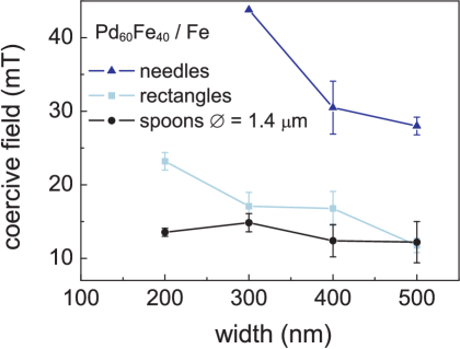
Both effects are illustrated by the data of Fig. 7, where we plot the coercive fields of strips ranging from to with and without an attached disc of diameter , or a needle tip. The disc clearly dominates the switching of the spoon-shaped structures and equals the coercive field of all strips around . However, for larger structures a stronger scatter in measured values can be observed. The needles show the strongest width dependence on the coercive field.
II.3.4 Effect of ferromagnetic supply lines
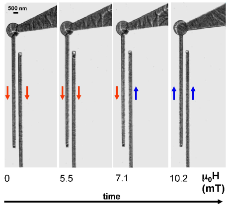
Fabricating contact electrodes together with supply lines and bond pads in a single metallisation process would simplify chip processing significantly. To investigate the effect of attaching large ferromagnetic supply lines on the magnetisation reversal of the contact electrodes, two identical strips with and without attached typical supply lines and bond pad (not shown) geometry attached are compared in Fig. 8. To reduce the magnetic coupling between electrode and supply lines a disk is placed at their junction. This disk typically forms a strongly diameter-dependent vortex, as discussed above.
Coming from saturation at high negative field, at (left panel in Fig. 8) both contacts have their magnetisation aligned downwards (red arrows). At , initiated by edge domains, the strip without attachment aligns along the external field (blue arrow). The strip with attachment follows at a coercive field of – in this particular case at a higher rather than at lower field value, as also observed with an attached disc structure. Still, there is a difference in coercive field of indicating that the magnetisation reversal is triggered by the multi-domain configuration in the supply lines. Switching is rendered irreproducible due to the random domain structure in the bulky supply line.
II.4 Temperature dependence
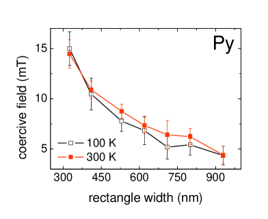
Low temperatures are still an important prerequisite to many fundamental studies of spintronics devices. This raises the question whether the results obtained by room temperature Lorentz microscopy remain valid in the low-temperature regime. For this purpose, Fig. 9 compares the coercive fields of rectangular Py strips obtained at room temperature with those at , the lowest accessible temperature in our TEM sample holder. Coercive field values agree, within the margin of error, for both temperatures, justifying an extrapolation of our findings to the low-temperature limit.
III Application in magnetotransport measurements
For electronic transport experiments, we have fabricated SWCNT samples with rectangular electrodes made from as well as MWCNT samples with electrodes made from , Py and a magnetic bilayer. The magnetoresistance was measured both in an in-plane magnetic field along the electrodes and also in a perpendicular, out-of-plane field.
III.1 Fabrication of nanotube devices
SWCNTs have been grown by chemical vapour deposition (CVD) on highly p-doped Si wafers with thermal oxide. The substrate can serve as backgate electrode. As feed gas we use a mixture of methane and hydrogen at with , and as catalyst.Kong et al. (1998) Best results were obtained with a flux of and a flux of although these parameters seem to be specific for the individual setup.
For the purposes of fabricating an individual SWCNT device, defect-free, clean nanotubes were located with respect to pre-patterned alignment markers using either scanning electron microscopy (SEM) or atomic force microscopy (AFM). In addition, high purity arc-discharge grown MWCNTs with typical diameters around were dispersed on wafers from solution and localized similarly. The fabrication of contact electrodes was adapted to the nanotube location by electron beam lithography and thin film deposition.
III.2 Room-temperature interface resistance of different ferromagnetic electrode materials to carbon nanotubes
While the magnetic domain structure of the contact electrodes is one defining factor for the performance of a CNT pseudo spin valve device, the nanotube contact resistance is another important material selection criterion.
A severe disadvantage of Py electrodes was their lack in interface quality to carbon nanotubes. In most devices, contact resistances of several were observed. Annealing for about at and improved the room temperature resistance of MWCNT samples temporarily; applying, to the same end, a large bias voltage of led to a significant drop of the resistance of the tube-metal interface. However, the interface deteriorated again on a scale of several days. Even while temporarily decreased the sample resistance was marked by strong fluctuations and abrupt jumps.
Palladium is known to form high-transparency contacts to carbon nanotubes.Javey et al. (2003b) Correspondingly it has also been shown that palladium-diluted ferromagnetic materials inherit this property.Man et al. (2006); Sahoo et al. (2005b); Kim et al. (2002); Hauptmann et al. (2008) Yet we found that even four electrodes patterned on the same tube in the same lithography and evaporation process can have highly different room temperature contact resistances, ranging from to the range. While some CNT devices with PdFe contacts yielded transparent contacts to carbon nanotubes, e.g. accessing the Kondo regime, the controllability of the magnetic domain configuration in this material remains insufficient.
In order to preserve the benefit of the low-resistive PdFe-CNT interface and to simultaneously obtain strong in-plane magnetisation, the aforementioned magnetic bilayer films consisting of and a -thick Fe layer were used. The contacting of carbon nanotubes with electrodes proved to be less reliable than with only. Resistances were typically in the -range. With an annealing step, the resistance of some samples could be reduced to room temperature values of down to . The noise level was high compared to the other two investigated contact materials. Characteristic for these samples was the occurrence of random telegraph noise-like resistance jumps, exceeding any magnetoresistance features by a factor of typically 2-3.
III.3 Low-temperature magnetoresistance measurements on SWCNTs
III.3.1 TMR in a parallel magnetic field
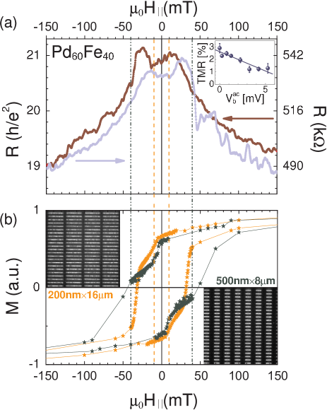
Fig. 10(a) shows the two-terminal resistance of a SWCNT pseudo spin valve with rectangular electrodes. It is plotted as a function of the external magnetic field during a field upsweep (light blue curve) and downsweep (dark red curve) from saturation of the electrodes to saturation in opposite field direction. The external magnetic field was aligned along the length of the electrode strips. On top of background features, a positive TMR signal emerges as a step-like increase in resistance within an interval of . It arises from the relative magnetisation orientation of narrow and wide electrodes.
The amplitude of the tunneling magnetoresistance was inferred from measurements of the two-terminal resistances and in parallel and antiparallel magnetisation orientation of the two ferromagnetic electrodes. We obtain a TMR effect of up to on top of a larger background magnetoresistance that is probably due to electron-magnon scattering. In some cases we observed a less significant maximum before reaching zero field, see e.g. the downsweep in Fig. 10(a). Its origin remains unclear at present. However, it seems to be absent when applying an out-of-plane field, compare Fig. 11.
III.3.2 magnetisation reversal from SQUID measurements of ferromagnetic strips
To confirm that the observed magnetoresistance features indeed originate from magnetic switching of the electrodes, we determined the coercive fields of typical thin-film contact electrodes at cryogenic temperature as a control experiment. Fig. 10(b) shows the hysteresis in magnetisation of narrow (orange) and wide (dark green) rectangles during up- and downsweep of an external magnetic field parallel to the strip axis. The signal was detected using a commercial SQUID magnetometer. To obtain a sizable magnetic moment, arrays of several ten thousand identical strips were EBL-patterned as shown in the insets of Fig. 10(b).
The curves clearly show more features than the sharp and rectangular hysteresis which would be expected from an ideal single domain switching event along a magnetically easy axis. The multiple features suggest multiple domain switching, but may also stem partially from end domain configurations, which do not impact the spin injection and detection in the tube (see e.g. the Lorentz microscopy images of Fig. 4). Still, when comparing the SQUID data with the magnetotransport measurements, as indicated by the dashed dark green and orange lines in Fig. 10, the switching of magnetoresistance for both sweep directions can be matched to the sharp features in the magnetisation curves. This is consistent with our findings from Lorentz microscopy that the wide electrode (dark green) has lower coercive field than the narrow one (orange) by shape anisotropy.
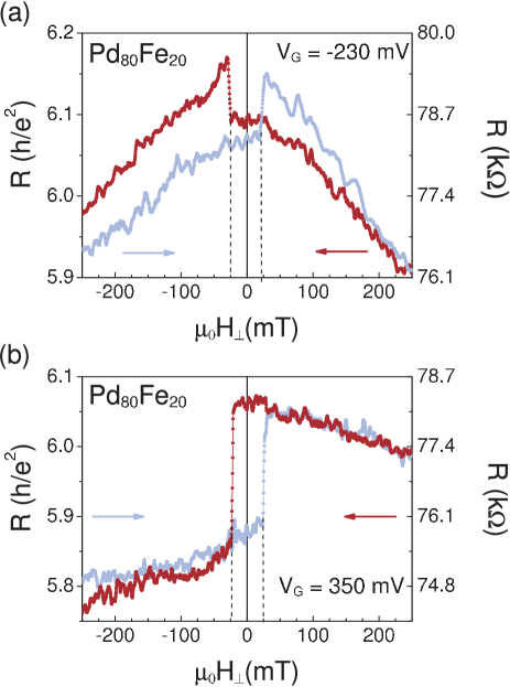
III.3.3 TMR in a perpendicular magnetic field
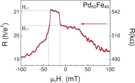
Fig. 11 displays an exemplary magnetoresistance downsweep on the same sample as shown in Fig. 10, in a different cooling cycle, now applying a magnetic field perpendicular to the sample plane. The resulting magnetoresistance curve displays a lower noise level and a clearer TMR feature with steeper flanks of up to is observed. This finding stands in contradiction to the assumption that the out-of-plane magnetisation component is negligible in thin ferromagnetic films. It is consistent, however, with our observation of cross-tie domain walls in these films in Lorentz microscopy, hinting at a non-negligible out-of-plane magnetisation. The switching is sharper than in parallel field, suggesting that the strips flip from one single-domain state to the other with fewer or no intermediate multi- or ripple domain states. The easy out-of-plane magnetic axis may also be the cause for the higher noise-level in parallel field magnetoresistance sweeps, due to a less well-defined and potentially fluctuating domain configuration.
III.4 Low-temperature magnetoresistance measurements on MWCNTs
III.4.1 TMR in a parallel magnetic field
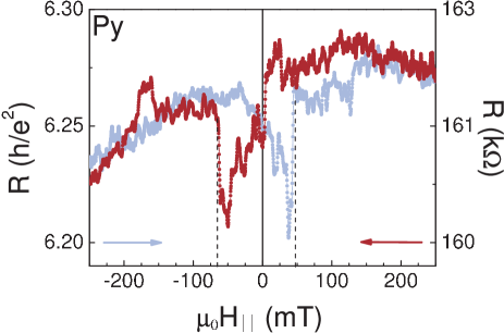
An example of the two-terminal resistance of a MWCNT pseudo spin valve with Py electrodes is shown in Fig. 12. The differential resistance is plotted as a function of magnetic field parallel to the length of the electrodes. The measurement displays negative TMR features of about for both up- and downsweep within the intervals and . As observed in many of our Py or samples, the measurement suffers from a high noise level. Unlike the clear TMR feature of Fig. 12, in many devices random telegraph noise was observed, where the resistance switched sharply between two or more distinct values. These jumps were irreproducible in subsequent magnetosweeps and typically higher in magnitude than the TMR features, limiting the reproducibility of the magnetoresistance curves.
III.4.2 TMR in a perpendicular magnetic field
Two exemplary magnetoresistance sweeps of a MWCNT pseudo spin valve as a function of an out-of-plane magnetic field are presented in Fig. 13. Also here an out-of-plane field is found to cause significant magnetoresistance effects. Fig. 13(a), recorded at , displays a hysteretical behaviour in the sense that at there is a sharp increase in resistance for up- and downsweep. The return from this positive TMR feature in antiparallel electrode magnetisation alignment down to the resistance in parallel alignment is gradual indicating a gradual shift of domain walls rather than sharp switching.
In contrast, Fig. 13(b), recorded at , exhibits only a single switching event per sweep at . Up- and downsweep are still hysteretical but no longer symmetric with respect to the axis. The resistance increases for the upsweep and decreases for the downsweep between two distinct resistance levels. Although it occurs at roughly the same magnetic field value as the first switching event in (a), this behaviour can not be explained with a change in resistance due to a simple realignment of two ferromagnetic electrodes from parallel to antiparallel magnetisation. The symmetric occurrence at hints that magnetic switching may stem from only one of the ferromagnetic electrodes whereas in the other electrode, the magnetisation is pinned probably by lattice defects, e.g. grain boundaries. So far the origin of the apparent gate dependence in Fig. 13 can not be accounted for. It may be a specific feature of MWCNTs since it was not observed yet in SWCNTs.Man et al. (2006); Sahoo et al. (2005b)
IV Conclusions
In conclusion, we have investigated various aspects of carbon nanotube-based pseudo spin valves with diluted ferromagnetic contacts.
Ferromagnetic contact electrodes of different shapes and materials were studied for their suitability as contacts for carbon-nanotube based pseudo spin valves using TEM Lorentz microscopy. This allowed the identification of materials and shapes that are in a magnetic single domain state and whose magnetisation switches at a sharp, reproducible and shape-tunable coercive field.
Permalloy structures displayed the required single-domain magnetisation reversal. In comparison, alloy strips switched their magnetisation via multi-domain configurations. This can account for the comparatively lower reproducibility in magnetisation reversal. Furthermore, cross-tie domain walls were observed as indication of a non-negligible out-of-plane magnetisation. Multiple fine ripple domains appeared in magnetic double layer structures made from .
For all electrode shapes investigated, it holds that a larger width lowers the coercive field. End domains were identified to act as seeds for magnetisation reversal and thereby to decrease the coercive field. Out of the electrode shapes investigated here, rectangular strips exhibited the most reliable magnetisation reversal, although a more pronounced end domain structure was observed compared to pointy and circular end shapes. Large-area ferromagnetic appendices to electrode strips, as in the case of attached disks or supply lines, were found to strongly impact the magnetic switching, and to lead to unpredictable behaviour.
Regarding the contact resistance to nanotubes, the properties of PdFe alloys were found to be significantly better than Py. Device resistances still varied strongly even along the same nanotube. SQUID measurements on large ensembles of same-sized electrode structures confirmed the coercive field scale.
Consistent with previous findings both positive and negative TMR featuresMan et al. (2006); Sahoo et al. (2005b) were observed. Using PdFe alloy electrodes of thickness, we were able to observe TMR for both in-plane and out-of-plane magnetic field direction, confirming the findings from Lorentz microscopy that the out-of-plane magnetisation is non-negligible in such contacts.
The giant paramagnet Palladium seems the obvious base material for carbon nanotube-based spintronics devices. Yet, the thin film magnetic properties of different ferromagnet-Pd alloys can vary strongly, in particular concerning the out-of-plane magnetisation, and require further optimisation.
We would like to thank H. S. J. van der Zant, A. Morpurgo, and B. Witkamp for helping us set up our CVD system, L. Forro and C. Miko for providing the multi-walled carbon nanotubes, and M. Aprili for fruitful discussion. Thanks also go to E. Lipp for proofreading. This work was supported by the DFG within the SFB 689 and the EU FP6 CARDEQ project.
References
- Prinz (1998) G. A. Prinz, Science 282, 1660 (1998).
- Cottet et al. (2006) A. Cottet, T. Kontos, S. Sahoo, H. T. Man, M. S. Choi, W. Belzig, C. Bruder, A. F. Morpurgo, and C. Schönenberger, Semic. Sci. and Techn. 21, S78 (2006).
- Hauptmann et al. (2008) J. R. Hauptmann, J. Paaske, and P. E. Lindelof, Nat. Phys. 4, 373 (2008).
- Buitelaar et al. (2002) M. R. Buitelaar, A. Bachtold, T. Nussbaumer, M. Iqbal, and C. Schönenberger, Phys. Rev. Lett. 88, 156801 (2002).
- Man et al. (2006) H. T. Man, I. J. W. Wever, and A. F. Morpurgo, Phys. Rev. B 73 (2006).
- Javey et al. (2003a) A. Javey, J. Guo, Q. Wang, M. Lundstrom, and H. Dai, Nature 424, 654 (2003a).
- Stirling et al. (1972) W. G. Stirling, R. A. Cowley, and M. W. Stringfellow, J. Phys. F: Metal Physics 2, 421 (1972).
- Sahoo et al. (2005a) S. Sahoo, T. Kontos, C. Schönenberger, and C. Sürgers, Appl. Phys. Lett. 86, 112109 (2005a).
- Zhao et al. (2002) B. Zhao, I. Mönch, T. Mühl, H. Vinzelberg, and C. M. Schneider, J. Appl. Phys. 91, 7026 (2002).
- Sahoo et al. (2005b) S. Sahoo, T. Kontos, J. Furer, C. Hoffmann, M. Graber, A. Cottet, and C. Schönenberger, Nat. Phys. 1, 99 (2005b).
- Julliere (1975) M. Julliere, Physics Letters A 54, 225 (1975).
- Kim et al. (2002) J.-R. Kim, H. M. So, J.-J. Kim, and J. Kim, Phys. Rev. B 66, 233401 (2002).
- Chapman (1999) J. Chapman, Journal of Magnetism and Magnetic Materials 200, 729 (1999).
- Lim (2002) C. Lim, Journal of Magnetism and Magnetic Materials 238, 301 (2002).
- Uhlig and Zweck (2004) T. Uhlig and J. Zweck, Phys. Rev. Lett. 93, 047203 (2004).
- Hubert and Schäfer (1998) A. Hubert and R. Schäfer, Magnetic Domains (Springer, 1998), 1st ed.
- Gomez et al. (1999) R. D. Gomez, T. V. Luu, A. O. Pak, K. J. Kirk, and J. N. Chapman, J. Appl. Phys. 85, 6163 (1999).
- Shalyguina et al. (2002) E. E. Shalyguina, K. H. Shin, and N. M. Abrosimova, Journal of Magnetism and Magnetic Materials 239, 252 (2002).
- Yu et al. (1999) J. Yu, U. Rüdiger, L. Thomas, S. S. P. Parkin, and A. D. Kent, J. Appl. Phys. 85, 5501 (1999).
- Kirk et al. (1999) K. J. Kirk, J. N. Chapman, and C. D. W. Wilkinson, J. Appl. Phys. 85, 5237 (1999).
- Huber (2005) M. Huber (2005), unpublished work.
- McCartney and Smith (1997) M. R. McCartney and D. J. Smith, Scanning Microscopy 11, 335 (1997).
- Kong et al. (1998) J. Kong, H. T. Soh, A. M. Cassell, C. F. Quate, and H. Dai, Nature 395, 878 (1998).
- Javey et al. (2003b) A. Javey, J. Guo, Q. Wang, M. Lundstrom, and H. Dai, Nature 424, 654 (2003b).