Coherent Oscillations and Giant Edge Magnetoresistance in Singly Connected Topological Insulators
Abstract
The topological insulators have a gap in the bulk but extended states at the edge that can carry current. We study a geometry in which such edge states will manifest themselves through periodic oscillations in the magnetoconductance of a singly connected sample coupled to leads through narrow point contacts. The oscillations occur due to quantum interference of helical edge states of electrons traveling along the circumference of the sample, and have a period of , where is the effective area enclosed by the edge states of the sample. Our calculation indicates the possibility of a large change in the magnetoresistance at small , termed giant edge magnetoresistance, which can have potential for application. The zero field conductance also exhibits oscillations as a function of the Fermi energy due to interference between edge states. The amplitude of the oscillations is governed by, and therefore can be used to investigate, the transverse width of the edge channels.
pacs:
73.23.-b, 73.43.Qt, 72.25.-bTopological insulators differ from ordinary insulators in having a pair of extended helical edge states, which results in quantum spin Hall (QSH) effect Kane05prl ; Bernevig06SCI ; Konig07SCI . Several candidates for topological insulators have been proposed, and a non-zero conductance has been measured experimentally in the ”inverted”-band semiconductor HgTe/CdTe quantum well in a band insulating region.Konig07SCI More experiments are beginning to explore the edge and surface state properties in topological insulators.Hsieh08Nature ; Wells09PRL ; Qi09SCI ; Hou09prl ; Yokoyama09xxx A direct observation of extended edge states would be important to establish the physics of topological insulators, and one may ask if they can also exhibit other interesting phenomena. We demonstrate that an effective one-dimensional ring is formed between two consecutive scatterers, which leads to Aharonov–Bohm (AB) oscillations in conductance. An observation of such oscillations in a singly connected geometry will constitute a direct observation of edge transport. Such oscillations are analogous to similar oscillations in singly connected quantum Hall systems Sivan89prb ; Wees89prl ; Jain88prl , but with an important difference: in the present case, the oscillations occur at very small magnetic fields. Our results also indicate the possibility of a ”giant edge magnetoresistance” (GEMR), which is insensitive to the geometry of the device and may have potential for practical application.

We study here the device shown in FIG.1, which consists of a two-dimensional strip of a topological insulator on which two quantum point contacts (QPCs) have been patterned thorough gates (shaded regions in FIG. 1). The QPCs define a saddle shaped confining potential, whose height can be controlled by a gate voltage. An effective disk of area ( is the radius of the disk) is formed in the center. An AB effect in the device can be expected intuitively because a topological insulator possesses a pair of independent gapless edge states of different spins moving in opposite directions, each forming an ideal one-dimensional loop around the disk. The two edge states are independent because no backscattering is allowed at a given sample edge even in the presence of weak time-reversal invariant disorder. We note here that spin is not a good quantum number in topological insulators because of spin orbit coupling. In the absence of a magnetic field, the actual edge states are eigenstates of the time reversal operator; their characterization as spin up and down is not precisely correct, and the word “spin” below is to be viewed more generally as the quantum number denoting the two states of a Kramers doublet. The effect of magnetic field, which breaks time reversal symmetry, is complicated. In our considerations below we assume that the magnetic field is sufficiently weak that the Zeeman term can be neglected; in that limit, the field does not open any gap in the spectra for the edge states, as discussed in detail in Ref. Zhou08prl .
In the remainder of the article we study this geometry quantitatively. We will assume that the weak magnetic field is normal to the plane. Following Ref. Sivan89prb we consider a spin-up (or spin-down) electron travelling from the left hand side (LHS) in FIG. 1. At the LHS junction it splits into two partial waves: one is transmitted through the QPC into the disk with amplitude , and the other is transmitted across the QPC with an amplitude causing a backscattering. We denote the wave function amplitudes in the upper edge and lower edge, right after the LHS junction, by and , respectively. The corresponding amplitudes in the vicinity of RHS junction are and , where , a fundamental unit of magnetic flux, is the magnetic flux threading the effective one-dimensional loop with an effective radius , and is the phase acquired by the wave function traveling along the loop . A partial wave goes through the RHS slit with an amplitude and across the slit with an amplitude . To simplify the problem, we assume identical reflection and transmission amplitudes for the two slits, and . Using the theory of multi-scattering processes Datta it then follows that the total transmission for spin-up electron through the slit A and B is given by
| (1) |
Here is the transmission coefficient of an electron through a slit, and Resonant tunneling occurs for , i.e., for any . The transmission coefficient for a spin-down electron which is the time reversal counterpart of spin-up electron at field, is given by . According to the Landauer-Buttiker formula,Landauer ; Buttiker the total conductance is
| (2) |
The AB oscillations in the conductance as a function of the magnetic flux through the disk are therefore expected to be symmetric with respect to the direction of the magnetic field.
To make further progress, we undertake a numerical calculation for the specific case of an “inverted”-band HgTe/CdTe heterojunction. We consider with the effective Hamiltonian for HgTe/CdTe quantum wellBernevig06SCI
| (3) |
where, in the spin-up sector, and is the wave vector in two dimension, is the Pauli matrix vector. , , and are sample specific parameters, and are functions of the thickness of the quantum well; here we take meV nm2, meVnm2, meVnm2, meV. In the spin-down sector is the time reversal counterpart of . The existence of edge states in this model has been discussed previously.Konig08JSPS ; Zhou08prl
To determine the conductance through the disk subjected to a perpendicular and weak field , we use the Keldysh Green function technique to calculate the transmission coefficients numerically in the Landauer-Büttiker formalismDatta . For this purpose, we use a tight-binding model that reproduces the Hamiltonian in Eq. (3) in the continuum limit, and include the magnetic field through the substitution ( is the vector potential). In the present work, more lattice sites and the lattice space nm were used in the calculation, and the lattice size effects are vanishingly small, so all results reported here reflect the continuum limit.

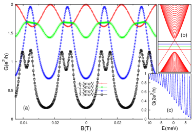
FIG. 2 shows the conductance for several Fermi energies, whose locations in the band structure are illustrated in FIG. 2(b). The conductance exhibits periodical oscillations in , with the period determined by the magnetic flux. For most parameters, the maximal value of the conductance does not reach because and in general do not satisfy the resonance condition simultaneously. A new feature is the rapid oscillations in the conductance at as a function the Fermi energy , as shown in FIG. 2(c). These oscillations are caused by the phase shift where the dispersion of the edge state meV ( in unit of nm-1) is linear in . The increasing oscillation amplitude reflects that the spatial distribution of edge state is dependent on the Fermi energy. Accordng to Zhou et al.Zhou08prl the spatial distribution of the edge state near the boundary has the form where and nm ( in units of meV) near the crossing point for the parameters adopted in this paper. Because we typically have , the spatial distribution of the edge state is determined dominantly by . Thus the edge state becomes wider with increasing energy, ultimately evolving into a bulk state when meV. Correspondingly, the transmission coefficients decreases and the oscillation amplitude increases according to Eq.(1).

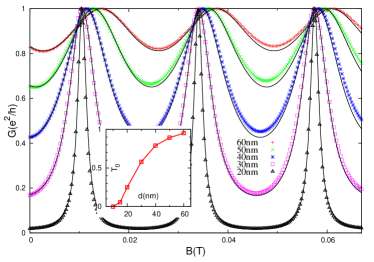
FIG. 3 shows the dependence of oscillations on the slit width . The solid lines are the best fits from Eq.(1) with three adjustable parameters , and The effective radius can be deduced from the period of the oscillation; its ratio to the radius of the disk is which reflects the finite width of an edge state near the boundary of the disk. The inset in FIG. 3 shows how depends on the slit width . As expected, vanishes for and approaches unity for . Conductance oscillations are suppressed in both limits; in particular, for it has the universal value Kane05prl ; Bernevig06SCI and displays no magnetoresistance. The AB oscillations occur only when the slit width is comparable to the spatial distribution of edge state. The numerical results are in good agreement with Eq.(1) in the first one or two periods, but exhibit an increasing deviation for a larger field , which may originate from the neglect, in our fits, of the dependence of the energy dispersion of the edge states on magnetic field (we use the dispersion when fitting the numerical data).

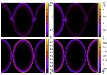
The quasi-one dimensional quantum interference behavior can be further illustrated by plotting the spatial profile of local current and the local density of states in a nonequilibrium situationLi07prb , where Fermi surface is slightly higher in the left lead so that the electrons flow from left to right. Current flow patterns for the up spin sector are shown in Figs. 4(a) and 4(b). The current flows only along the boundary of the device with definite chirality (see FIG.1). At the resonance transmission , the backward current reflection at QPC A is totally suppressed, which corresponds to a peak in the magnetoresistance oscillations. The maximum reflection is observed at the valley of the oscillations. When a resonance transmission occurs, the maximum of local density of states is found in the central disk edge while, at minimum transmission, the maximum local density of states is observed in the terminals.

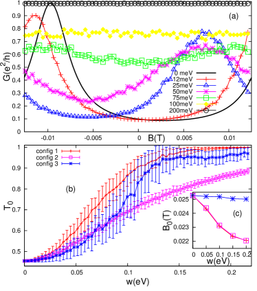
The feasibility of the observations of the predicted magnetoresistance oscillations depends in part on how sensitive their amplitude is to the ever present disorder. Given that time reversal invariant disorder does not cause any backscattering between two spin channels at the same edgeKane05prl ; Wu06prl ; Xu06prb , one might expect that it also does not affect the coherent magnetoresistance oscillations. We study the effect of disorder by introducing disorder as a random on-site energy with a uniform distribution within . The results, displayed in FIG. 5(a), demonstrate that disorder diminishes the amplitude of oscillations while enhancing the average conductance. The reduction of the coherent oscillations originates from an impurity configuration dependent phase shift in Eq. (1); the disorder averaging over the phase shift smears the quantum interference, completely suppressing it when the variance of is comparable with . It is noteworthy that the AB oscillations survive up to quite large disorder. For comparison, the hopping matrix element in Eq.(3) is meV, and numerical results indicate that the oscillation is almost suppressed when the on-site disorder . The enhancement of the average conductance is surprising at first sight (see FIG. 5(b)), but we attribute it to a squeezing the spatial distribution of the edge states by disorder. Such squeezing can also be seen in the slight decreasing of the oscillation period of the conductance with large disorder strength as the effective radius (see the insert in FIG. 5(b).). Also the disorder around the slit can increase the tunneling probability as the higher disorder can close the energy gap (caused by the finite size of the slit) near the Fermi surface Beverly02PNAS . Of course, even stronger disorder leads to the Anderson localization, and the edge states will be destroyed Li09prl ; Onoda07prl ; Sheng06prl , resulting in a lack of conductance.
All our preceding discussion assumes strictly zero temperature. Scattering between the spin up and spin down edges becomes possible at nonzero temperatures due to inelastic scattering involving phonons, which is believed to cause the deviation from perfect quantization in the experiments of Ref. Konig07SCI . The AB oscillations discussed above will be observable only for disks with perimeters less than the phase coherence length of the edge states.
In conclusion, we have studied theoretically a geometry in which the edge states of topological insulators are predicted to produce coherent oscillations in the magnetoconductance due to Aharonov-Bohm interference. This physics also produces a giant edge magnetoresistance in a weak field; FIG. 2 shows that the conductance may change by an order of magnitude for a tiny field T. If confirmed by experiments, this may be of practical interest. The giant edge magnetoresistance can be controlled by varying the slit width and the size of the disk. We have also studied its sensitivity to disorder, and found that it persists for quite large disorder. The amplitude of AB oscillations also contains information about the transverse spatial extent of the edge channels.
This work was supported by the Research Grant Council of Hong Kong under Grant No.: HKU 703708, and HKU 10/CRF/08.
References
- (1) C. L. Kane and E. J. Mele, Phys. Rev. Lett. 95, 226801(2005); ibid. 95 146802 (2005)
- (2) B. A. Bernevig et al., Science 314, 1757 (2006).
- (3) M. Konig et al., Science 318, 766 (2007).
- (4) D. Hsieh et al., Nature (London) 452, 970 (2008); Science 323, 919 (2009)
- (5) J. W. Wells et al., Phys. Rev. Lett. 102, 096802 (2009)
- (6) X. L. Qi et al., Science 323, 1184 (2009); Nature Physics 4, 273 (2008)
- (7) C. Y. Hou et al., Phys. Rev. Lett. 102, 076602 (2009)
- (8) T. Yokoyama et al., arXiv: 0901.0438
- (9) J. K. Jain, Phys. Rev. Lett. 60, 2074 (1988).
- (10) U. Sivan et al., Phys. Rev. B 39, 1242 (1989)
- (11) B. J. van Wees et al., Phys. Rev. Lett. 62, 2523 (1989).
- (12) B. Zhou et al., Phys. Rev. Lett. 101, 246807 (2008)
- (13) S. Datta, Electronic Transport in Mesoscopic Systems (Camberidge University Press, London, 1995), pp. 129, 296-321.
- (14) R. Landauer, Phil. Mag. 21, 863 (1970).
- (15) M. Büttiker, Phys. Rev. B 38, 9375 (1988).
- (16) M. König et al., J. Phys. Soc. Jpn. 77, 031007 (2008).
- (17) J. Li et al., Phys. Rev. B 76, 153302 (2007).
- (18) K. C. Beverly et al., Proc Natl Acad Sci USA 99, 6456 (2002)
- (19) J. Li et al., Phys. Rev. Lett. 102, 136806 (2009)
- (20) C. Wu et al., Phys. Rev. Lett. 96, 106401 (2006)
- (21) C. Xu and J. E. Moore, Phys. Rev. B 73, 045322 (2006)
- (22) M. Onoda et al., Phys. Rev. Lett. 98, 076802 (2007).
- (23) D. N. Sheng et al., Phys. Rev. Lett. 97, 036808 (2006)