Leakage Currents and Capacitances of Thick CZT Detectors
Abstract
The quality of Cadmium Zinc Telluride (CZT) detectors is steadily improving. For state of the art detectors, readout noise is thus becoming an increasingly important factor for the overall energy resolution. In this contribution, we present measurements and calculations of the dark currents and capacitances of 0.5 cm thick CZT detectors contacted with a monolithic cathode and 88 anode pixels on a surface of 22 cm2. Using the NCI ASIC from Brookhaven National lab as an example, we estimate the readout noise caused by the dark currents and capacitances. Furthermore, we discuss possible additional readout noise caused by pixel-pixel and pixel-cathode noise cross-coupling.
Index Terms:
CZT, electronic noise, radiation detection.I Introduction
There are multiple applications for the room-temperature semi-conductor Cadmium Zinc Telluride (CZT), ranging from medical imaging over homeland security to astroparticle physics experiments. The high efficiency and good spectral and spatial resolution of CZT make it an attractive material for detecting and measuring photons in the energy range from a few keV to a few MeV. As the fractional yield of high-quality crystals increases (and the cost is reduced), CZT will become even more prolific in radiation detection systems.
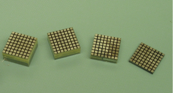
Limits on the performance of of CZT detector systems depend on characteristics of both the detector and the readout electronics. State-of-the-art CZT detectors combine excellent homogeneity over typical volumes between 0.522 cm3 and 1.522 cm3 with high electron -products on the order of cm2 V-1. As the best thick CZT detectors achieve now 662 keV energy resolutions better than 1% FWHM (full width half maximum), low-noise readout becomes increasingly more important. In the following, we will present leakage current and capacitance measurements performed on CZT detectors from the company Orbotech Medical Solutions [1]. Orbotech uses the Modified Horizontal Bridgman process to grow the CZT substrates. The process gives substrates with excellent homogeneity, but a somewhat low bulk resistivity of 109 cm. In earlier work, several groups including ourselves have shown that pixel-cathode dark currents can be suppressed efficiently by contacting the substrates with high-work function cathodes [2, 3]. We are currently testing Orbotech detectors with a wide range of thicknesses and with a range of pixel pitches (see Fig. 1, and Qiang et al., 2007). In this contribution, we present measurements of the dark currents and capacitances of an Orbotech CZT detector (0.522 cm3, 88 pixel,2.4mm pitch, 1.6mm pixel side-length), and discuss the resulting readout noise. In Sect. 2, the ASIC used as a benchmark for noise calculations is described, and the noise model parameters are given. The results of dark current and capacitance measurements are described in Sect. 3. In Sect. 4 the resulting noise is estimated, and in Sect. 5 pixel-pixel and pixel-cathode noise cross-coupling is discussed. In Sect. 5, the results are summarized.
II Noise Model
As a reference for our noise calculations, we use the “NCI ASIC” developed by Brookhaven National Laboratory and the Naval Research Laboratory for the readout of Si strip detectors (De Geronimo et al., 2007). The self-triggering ASIC comprises 32 channels. Each front-end channel provides low-noise charge amplification for pulses of selectable polarity, shaping with a stabilized baseline, adjustable discrimination, and peak detection with an analog memory. The channels can process events simultaneously, and the read out is sparsified. The ASIC requires 5 mW of power per channel.
We use the following noise model to calculate the equivalent noise charge (ENC):
| (1) |
where ,and characterize the pulse shaping filter, is the pulse peaking time, and are the detector and MOSFET capacitances, respectively, is the MOSFET transconductance, is the 1/f noise coefficient, is the detector leakage current, and is the parallel noise of the reset system (De Geronimo et al.,2002). For a given detector () and ASIC () can be optimized to reduce the ENC. For the NCI ASIC, we use [8, 5]: =0.89, ==0.52, =, =6pF, =8mS, and =50pA.
III Dark Current and Capacitance in Orbotech CZT Detectors
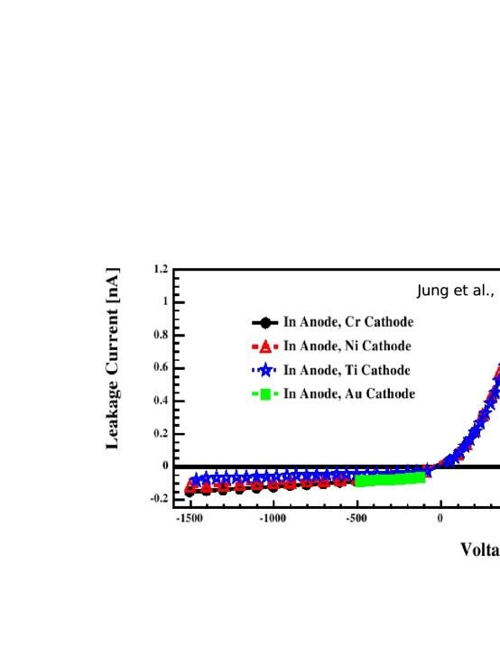
Figure 2 shows the IV curves for one 220.5 cm3 Orbotech CZT detector, for different cathode contact materials. The preferred cathode material is Au, as Au cathodes give leakage currents 0.2 nA/pixel at a cathode bias voltage of -1500 Volts, and give slightly better spectroscopic performance than other cathode materials.
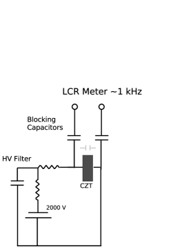
We used a commercial capacitance meter to measure the capacitance between all pixels and the cathode. The measurement set-up is shown in Fig. 3. High voltage blocking capacitors were used to protect the LCR meter from the detector bias voltage. A low pass filter was used to isolate the LCR-meter-detector circuit from the high voltage supply at the kHz frequencies used by the LCR meter. Largely independent of bias voltage, we measure a capacitance of 9 pF for all 64 pixels, corresponding to a pixel-cathode capacitance of 0.14 pF per pixel. The measured result agrees well with a simple estimate of the anode to cathode capacitance: using a dielectric constant of 10 [7], a parallel plate capacitor with the same dimensions as our detector has a capacitance of 8 pF.
The measurements of the pixel-pixel capacitances resulted in upper limits of 1 pF. For inner pixels (non-border pixels) we estimated the pixel-pixel capacitances with the same 3-D Laplace solver that we are using to model the response of CZT detectors from our fabrication [2]. The code determines the potential inside a large grounded box that houses the detector. The capacitance between one pixel and its neighbors is determined by setting the voltage of the one pixel to 1 V while keeping the other pixels and the cathode at ground potential. The charge on the biased pixel and on the neighboring pixels is determined with the help of Gauss’ law and appropriate Gaussian surfaces. The procedure gives the capacitances . We obtain a next-neighbor capacitance of 0.06 pF, and a diagonal-neighbor capacitance of 0.02 pF.
IV Equivalent Noise Charge of CZT ASIC Readout Electronics
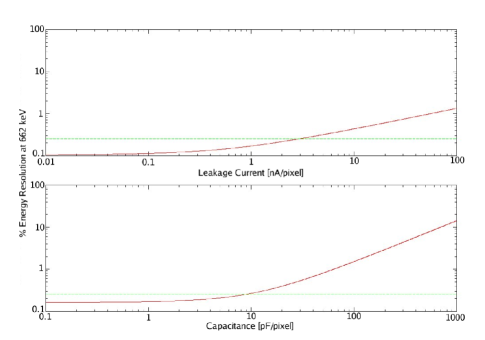
With the previous results, we can now evaluate Equation (1). In the context of 662 keV energy depositions (assuming 4.64 eV per electron-hole pair generation, [7]), Fig. 4 plots the FWHM contribution (red line) of the readout electronics’s ENC as a function of dark current (top) and pixel capacitance (bottom). For the upper plot, is held constant at 1.0 pF and for the lower plot was fixed at 1 nA. In both panels, the green line marks a readout noise contribution of 0.25% FWHM to the 662 keV energy resolution. At the 0.25%-level, the contribution of the readout noise to the detector energy resolution is negligible. For the specific ASIC considered here, we see that leakage currents up to 3 nA and pixel capacitances 10 pF are acceptable. The leads between the readout ASIC and the detector should be sufficiently short to stay below 10 pF.
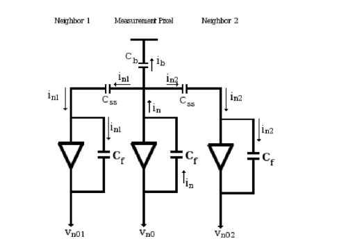
V Pixel-Pixel and Pixel-Cathode Noise Cross-Coupling
In this section we consider possible additional noise contributions arising from the capacitive coupling between adjacent pixels and between a pixel and the cathode. The capacitive coupling can result in amplifier noise from one channel being injected into the other channel. In the following we use the terminology used by Spieler (2005), and assume that all pixels and the cathode are read out by identical preamplifiers. We first consider pixel-pixel noise cross coupling (compare Fig. 5) and consider the coupling between a pixel, its four nearest neighbors and the cathode. The output noise voltage () of an amplifier creates a noise current, .
| (2) |
Here, , , and is the pixel-pixel capacitance, the pixel-cathode capacitance, and the amplifier capacitance, respectively. The current is divided among the capacitively coupled channels in proportion to the coupling capacitance. The fraction of going to a nearest neighbor is
| (3) |
Adding the additional noise from the four nearest neighbors in quadrature, we find that the pixel-pixel crosstalk will increase the electronic noise by:
| (4) |
. In most applications, one reads out the pixels and the cathode. For single-pixel events, the pixel-to-cathode signal ratio can be used to correct the anode signal for the depth of the interaction. For multiple-pixel events, the time offset between the cathode signal and the pixel signals can be used to perform a proper depth of interaction correction for each individual pixel. The pixel-cathode noise cross-coupling can be more significant. The equivalent noise charge from cathode noise being injected into pixels, , depends on the number of pixels () and the ratio of the feedback capacitance to the detector capacitance [7]:
| (5) |
Here =64 is the number of pixel, = 7 pF is the capacitance between the cathode and all the pixels, and =50 fF is the preamplifier feedback capacitance. With these values, the cathode noise can increase the readout noise of the anode channels by 68%.
VI Summary
We measured pixel-cathode dark currents and the pixel-cathode capacitances, both as function of detector bias voltage. The measurements give dark currents well below a nA per pixel, and a pixel-cathode capacitance of 0.14 pF per pixel.
The pixel-pixel capacitances were smaller than the accuracy of our measurements, and we determined them with the help of a 3D Laplace solver. We obtain the result that pixel-pixel capacitance is 0.06 pF for direct neighbors and 0.02 pF for diagonal neighbors. For a state-of-the-art ASIC as the NCI ASIC used as a benchmark here, the noise model predicts a very low level of readout noise. With these nominal capacitance values, pixel-pixel noise cross-coupling is a minor effect, but cathode-pixel noise cross coupling can be significant. In practice, the readout noise will be higher owing to additional stray capacitances from the detector mounting and the readout leads, and from pick-up noise. For the design of a readout system, short leads and a proper choice of the detector mounting board substrate are thus of utmost importance.
Acknowledgments
We gratefully acknowledge Gianluigi De Geronimo and Paul O’Connor for information concerning the NCI ASIC. This work is supported by NASA under contract NNX07AH37G, and by the DHS under contract 2007DN077ER0002.
References
- [1] Orbotech Medical Solutions LTd., 10 Plaut St., Park Rabin, P.O.Box: 2489, Rehovot, Israel, 76124.
- [2] I.V. Jung, A. Garson III, H. Krawczynski, A. Burger, B. Groza, 28, 397 (2007) [arXiv: 0710.2655].
- [3] Hong, J., et al., SPIE Conference Proceedings ÒHard X-Ray and Gamma-Ray Detector Physics IXÓ, 6706-10 (2007), in press [arXiv:0709.2719].
- [4] Q. Li, A. Garson III, I.V. Jung, M. Groza, P. Dowkontt, R. Bose, G. Simburger, A. Burger, H. Krawczynksi, Proc. 2007 IEEE Nucl. Sci. Symp., Hawaii, Oct. (2007).
- [5] G. De Geronimo, P. O’Connor, IEEE Trans. Nucl. Sci., 52, 3223 (2005).
- [6] G. De Geronimo, J. Fried, E. Frost, B.F. Phlips, E. Verrnon, and E.A. Wulf, Front-End ASIC for a Silicon Compton Telescope Proc. 2007 IEEE Nucl. Sci. Symp., Hawaii, Oct. (2007).
- [7] H. Spieler, Semiconductor Detector Systems, Oxford University Press (2005).
- [8] G. De Geronimo, P. O’Connor, A. Kandasamy, J. Grosholz, Proc SPIE 4784 (2002).