Voltage-tunable lateral shifts of ballistic electrons in semiconductor quantum slabs
Abstract
It is investigated that the lateral shifts of the ballistic electrons transmitted through a semiconductor quantum slabs can be negative as well as positive, which are analogous to the anomalous lateral shifts of the transmitted light beam through a dielectric slab. The necessary condition for the shift to be negative is advanced. It is shown that the lateral shifts depend not only on the structure parameters of semiconductor quantum slab, but also on the incidence angle and the incident energy. Numerical calculations further indicate that the lateral shifts can be tuned from negative to positive by the external applied electric field. The voltage-tunable lateral shifts may lead to potential applications in quantum electronic devices.
pacs:
73.23.Ad, 42.25.Gy, 73.63.HsI Introduction
The analogies between phenomena occurring in two different physical systems open a route to find new effects or to translate solution on techniques or devices, and quite often help to understand both systems better Dragoman . In particular, electronic analogues of many optical behaviors such as reflection, refraction Gaylord ; Gaylord-GB , focusing Houten ; Spector-S-K ; Sivan , collimation Molenkamp , and interference Yacoby ; Liang ; Ji have been achieved in two-dimensional electron gas (2DEG) enabling the systems as a basic platform to study foundation problems in quantum mechanics Buks ; Chang as well as quantum information processing Beenakker-EKV . The close relation between optics and electronics result from the fact that the electrons act as wave due to the ballistic transport properties of a highly mobility 2DEG created in semiconductor heterostructures Palevski . As a result, there is growing interest in the design and development of devices based on electron wave propagation, which have given rise to a research field described as electron wave optics Gaylord-Brennan-Gaylord-G-H ; Dragoman-D ; Datta .
Among those electric-optic analogies, the electric analogue of Goos-Hänchen (GH) effect have attracted much attention in recent years Wilson-G-G ; Zhao ; Beenakker ; Chen ; Chen-PRB , because of its practical significance in design of many new quantum electron devices. In 1993, Gaylord et al. Wilson-G-G once showed that the ballistic electrons totally reflected from a potential-energy/effective-mass interface experience a lateral shift from the position predicted by electron wave optics. This phenomenon is known as GH effect in optics Goos . Very recently, Zhao and Yelin Zhao have shown that, based on the electronic counterpart to the trapped rainbow effect in optics Tsakmakidis , the interplay GH effect and negative refraction Cheianov in graphene leads to the coherent graphene devices, such as movable mirrors, buffers and memories. Beenakker et al. Beenakker have further found that the GH effect at a - interface in graphene doubles the degeneracy of the lowest propagating mode, which can be observed as a stepwise increase by of the conductance with increasing channel width. As a matter of fact, the GH shifts for matter wave Renard ; Carter and even relativistic Dirac electrons Miller ; Fradkin have been considered previously. However, it is shown that the electric GH shift in total reflection is only about the order of the electron wavelength. The smallness of the GH shift has impeded its direct measurement and applications. In previous paper, we found that the lateral shifts of ballistic electrons in a semiconductor quantum barrier can be enhanced by transmission resonance, and are always positive Chen . It is further shown that the tunable lateral shifts in magnetic-electric nanostructure have some significant applications in spin filter and spin beam splitter Chen-PRB .
In present paper, we will investigate that the lateral shift of ballistic electrons transmitted through a semiconductor quantum well Gaylord-GB ; Wilson-G-G , acting as electron wave slab, can be negative as well as positive. The necessary condition for the lateral shift to be negative is given. The negative lateral shift presented here is similar to but different from a phenomenon of electronic negative refraction Cheianov ; Dragoman-JAP . Actually, the negative lateral shift is the electronic analogue to the negative lateral shift of a light beam transmitted through a dielectric slab Li . More importantly, it is found that the lateral shifts in a fixed semiconductor heterostructure can be modulated from negative to positive by the external applied electric field. This leads to some interesting applications in quantum electronic devices such as beam spatial modulation, beam splitter, and wave vector or energy filter.
II Lateral shifts in semiconductor quantum slab

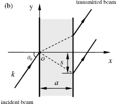
Consider ballistic electrons with the energy is incident obliquely upon a two-dimensional semiconductor quantum well, extending from to , as shown in Fig. 1, where , and and are the depth of potential well and the values of the potential energies on its two sides, respectively. The corresponding electron effective masses are and . The wave function of an incident electron beam can be expressed in terms of plane wave components as where , , is defined by Plank constant divided by , stands for the incident angle of the plane wave component under consideration, and is the amplitude angular-spectrum distribution of electron beam. If the angular spectral distribution is sharp enough, the wave function can be rewritten as
| (1) |
For a Gaussian-shaped incident beam whose peak is assumed to be located at ,
| (2) |
its angular spectral distribution is also a Gaussian function, , around its central , , is the width of the beam at waist. For a incident plane wave component , letting be the corresponding transmitted plane wave component, the transmitted beam at can be expressed by,
| (3) |
where the transmission coefficient is determined by the following complex number,
so that the phase shift can be expressed by
| (4) |
where , , and is determined by Snell’s law for electron wave, . For a well collimated beam, the lateral shift of the ballistic electrons in transmission the quantum slab is defined as Wilson-G-G ; Chen , according to the stationary phase method Bohm , and is thus given by
| (5) |
where , is determined by Snell’s law for electron wave, , is the geometrical shift predicted by electron wave optics, and is the transmission probability, which is closely related to the measurable ballistic conductance , according to the well-known Landauer-Büttiker formula Buttiker . It is noted that the subscript in this paper denotes the values taken at , namely . It is clear that the lateral shift is modulated by the transmission probability as is indicated in Eq. (5), thus is in general different from . More interestingly, when the necessary condition
| (6) |
since , the lateral shift can be negative when the restriction to the incidence angle ,
| (7) |
is satisfied. This means that if is larger than the threshold angle , one can always find a thickness of the quantum wells where the lateral shift of the transmitted beam is negative. Moreover, it is clearly seen that when the incident energy is in the region of
| (8) |
that is, , the necessary condition (7) is satisfied, so that the lateral shift of ballistic electrons in the quantum slab can be negative as well as positive. On the contrary, the lateral shifts in the case of are always positive, since the necessary condition (7) is invalid. In fact, when the semiconductor quantum barrier () is considered, the critical angle for total reflection is defined as,
| (9) |
Thus, the lateral shifts are always positive, as discussed in Ref. Chen . More interestingly, when is larger than the critical energy , we have critical angle , that is, the ballistic electrons can traverse through the quantum barrier at any incidence angle. In this case, the quantum barrier behaves as quantum slab for Wilson-G-G , thus the lateral shifts can be negative under the condition (7).
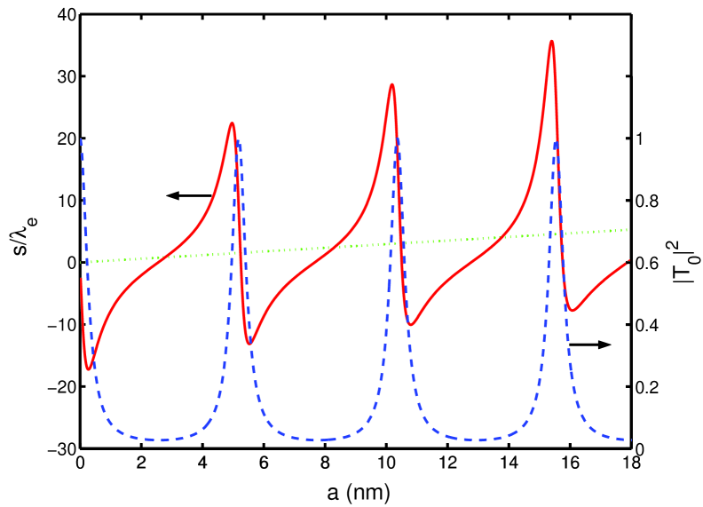
To illustrate the negative lateral shifts of ballistic electrons, the example semiconductor quantum well consisting of . The potential energies in the three regions of the quantum well are given by the conduction band edge as , and (in which the conduction band discontinuity has been taken to be of the energy gap change). The corresponding effective electron mass is , where is the free electron mass, and Wilson-G-G . Fig. 2 shows the typical dependence of the lateral shift (solid curve) and transmission probability (dashed curve) on the width in semiconductor quantum well , where , , , and , the incidence energy is , the incidence angle is , is in units of the wave length of free electron, , and the dotted curve represents the lateral displacement predicted from electron wave optics, . It is clear that the lateral shift is quite different from the lateral displacement predicted from electron wave optics, and can be negative. The negative shift is similar to but different from the negative refraction of ballistic electrons in graphene Cheianov or metamaterial Dragoman-JAP . This phenomenon results from the destructive and constructive interference of the electron waves due to the multiple reflections and transmissions inside the slab. As a matter of fact, the inequality (6) is required for the lateral shift to be negative. Since the function decreases rapidly with increasing , the width of the potential well should be of the order of , that is, the order of the wavelength , so as to make the negative lateral shift significantly large. As a result, the necessary condition for the width of quantum slab Chen
| (10) |
holds for the incident beam, the whole transmitted beam will maintain the shape of incident beam with negative lateral shift, that is to say, the stationary phase method is valid when the condition (10) is satisfied.
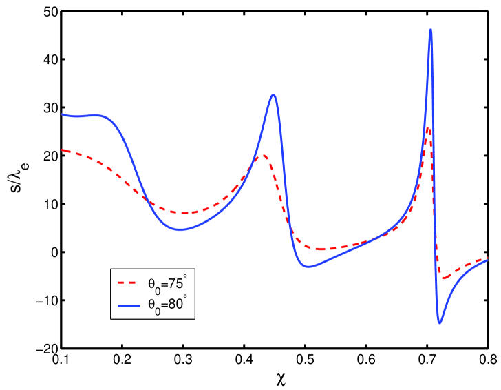
It should be pointed out that the physical structure of semiconductor quantum well has great impact on the lateral shift. Fig. 3 shows the dependence of the lateral shift on the parameter of the semiconductor quantum slab at different incidence angles, where , , , , and other physical parameters are the same as in Fig. 2. It is shown that the absolute value of lateral shift can be enhanced by increasing the physical parameter , which corresponds to the increase of the effective mass and potential energies in the two sides of quantum slab. In addition, Eq. (5) also indicates that the negative lateral shift also depends on the angle of incidence and the incident energy. Thus, the spatial location of the transmitted ballistic electrons can be altered by the negative and positive lateral shifts which can be easily controlled by the incidence angle or the incidence energy. In what as follows we will emphasize the modulation of the lateral shifts in a fixed semiconductor quantum structure by external electric field.
III Modulation by external applied electric field
In this section, we will focus on the control of the lateral shifts, taking account into imposing external electric field on the semiconductor quantum slab as shown in Fig. 1(a).
For a plane wave component of the incident ballistic electrons, the corresponding transmitted plane wave is given by in this case, where . Because the system is translationally invariant along the direction, the wave function in the region of the quantum well under applied electric field can be expressed as , where the longitudinal wave packet is determined by,
| (11) |
where is the longitudinal energy and is the applied biased voltage. The solutions of the above Schrödinger equation are the well-known linearly independent Airy functions and Mathematics , that is , where
Combining the boundary conditions, we can finally obtain the transmission coefficient determined by the following complex number
so that
| (12) |
where
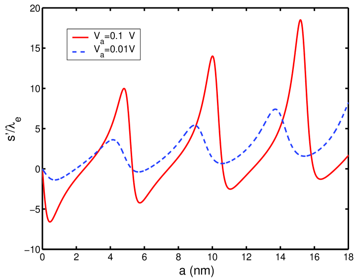
, , , and are the values of Airy functions and their derivations with respect to at and , respectively. According to the stationary phase method discussed above, the lateral shift of the ballistic electrons transmitted through a quantum slab under applied electric field is thus given by . By numerical calculations, Fig. 4 shows the lateral shifts of the ballistic electrons transmitted though a quantum slab under an external applied electric field , where (solid curve), (dashed curve), and the other physical parameters are the same as in Fig. 2. It is shown that the lateral shifts with biased voltage can also be negative as well as positive in the same way as those in absence of external applied electric field.
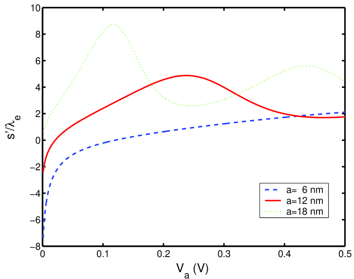
Next, we will discuss in detail on the effect of external applied electric field on the lateral shift. Fig. 4 shows the dependence of the lateral shift on the width of the semiconductor quantum slab under different applied electric fields. It is clearly seen that the lateral shifts changes dramatically when the biased voltage increases. In Fig. 5, the lateral shift can tuned from negative to positive under some conditions. It is further shown that it is more feasible to control the lateral shift by external applied electric field with increasing the width of the semiconductor quantum slab. In Ref. Chen-PRB , it has been shown that there exists a large negative lateral shift in magnetic-electric nanostructure. However, as in many previous proposals Chen ; Chen-PRB , the positive or negative lateral shifts of the ballistic electrons cannot be manipulated once one chooses the quantum semiconductor structure. Here we use the applied electric field to realize the modulation of the lateral shifts in a fixed semiconductor quantum well. Thus, it is a very useful and powerful way to control the spatial beam location of the ballistic electrons, which may lead to the potential applications in quantum electric devices, such as electric spatial modulation, beam splitter, and electron wave vector or energy filter Kan .
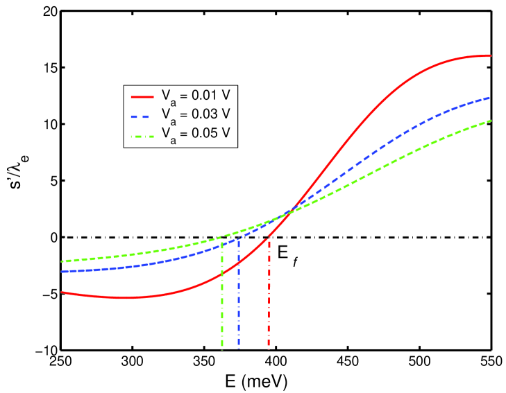
Finally, we have a brief look at the applications of tunable lateral shifts in various quantum electric devices. To this end, we represent an example of the spatial beam modulation and energy filter based on the voltage-tunable lateral shifts, as shown in Fig. 6, where , (solid curve), (dashed curve), (dash-dotted curve), and the other physical parameters are the same as in Fig. 2. Fig. 6 shows that the different incident energies of ballistic electrons correspond to their different lateral shifts in transmission. So the spatial beam location can be modulated by the incident energy under the different external applied electric fields. In addition, it is also shown in Fig. 6 that the lateral shift is positive for , while it is negative for . Furthermore, the threshold of energy corresponding to the lateral shift , which is measured by the spatial location , can be controlled by the biased voltage . Therefore, the energies of incidence electrons can be easily chosen by the positive or negative lateral shifts, which results in the energy filter. As a result, the quantum devices such as spatial modulation, beam splitter, and wave vector or energy filter can be realized by the controllable negative and positive lateral shifts, because of their dependence on incident energy and incidence angle.
IV Summary
In conclusion, the lateral shifts of the ballistic electrons transmitted through a semiconductor quantum well can be positive as well as negative. The necessary condition (7) is advanced here for the shift to be negative. The negative and positive lateral shifts, which is similar to but different from the negative refraction for ballistic electron, are analogous to those of the light beam transmitted through a dielectric slab. This semiconductor quantum slab discussed here behaves as the Fabry-Perot-type interferometer for ballistic electrons in the literature Liang . Therefore, the anomalous lateral shifts can be understood from the destructive and constructive interference due to the multiple reflections and transmissions inside the quantum slab. More importantly, the lateral shifts can be tuned from negative to positive when the external electric field is applied in a fixed semiconductor quantum structure. In a word, with development of semiconductor technology, the tunable lateral shifts of ballistic electrons may lead to the potential applications in various quantum electric devices.
Acknowledgments
This work was supported in part by the National Natural Science Foundation of China (60806041, 60877055), the Shanghai Rising-Star Program (08QA14030), the Science and Technology Commission of Shanghai Municipal (08JC14097), the Shanghai Educational Development Foundation (2007CG52), and the Shanghai Leading Academic Discipline Program (S30105).
References
- (1) Quantum-Classical Anologies, edited by D. Dragoman and M. Dragoman (Springer, Berlin, 2004).
- (2) T. K. Gaylord and K. F. Brennan, J. Appl. Phys. 65, 814 (1989).
- (3) T. K. Gaylord, E. N. Glytsis, and K. F. Brennan, J. Appl. Phys. 66, 1842 (1989).
- (4) H. van Houten, B. J. van Wees, J. E. Mooij, C. W. J. Beenakker, J. G. Williamson, and C. T. Foxon, Europhys. Lett. 5, 721 (1988).
- (5) J. Spector, H. L. Stormer, K. W. Baldwin, L. N. Pfeiffer, and K. W. West, Appl. Phys. Lett. 56, 1290, 2433 (1990); 58, 263 (1991).
- (6) U. Sivan, M. Heiblum, C. P. Umbach, and H. Shtrikman, Phys. Rev. B 41, R7937 (1990).
- (7) L. W. Molenkamp, A. A. M. Staring, C. W. J. Beenakker, R. Eppenga, C. E. Timmering, J. G. Williamson, C. J. P. M. Harmans, and C. T. Foxon, Phys. Rev. B 41, R1274 (1990).
- (8) A. Yacoby, M. Heiblum, V. Umansky, H. Shtrikman, and D. Mahalu, Phys. Rev. Lett. 73, 3149 (1994).
- (9) W. J. Liang, M. Bockrath, D. Bozovic, J.H. Hafner, M. Tinkham and H. Park, Nature 411, 665,(2001); C.T. White and T. N. Todornov, Nature 411, 649 (2001).
- (10) Y. Ji, Y. Chung, D. Sprinzak, M. Heiblum, D. Mahalu, and H. Shtrikman, Nature 422, 415 (2003).
- (11) E. Buks, R. Shuster, M. Heiblum, D. Mahalu, and V. Umansky, Nature 391, 871 (1998).
- (12) D.-I. Chang, G. L. Khym, K. Kang, Y. Chung, H.-J. Lee, M. Seo, M. Heiblum, D. Mahalu, and V. Umansky, Nature Phys. 4, 205 (2008).
- (13) C.W. J. Beenakker, C. Emary, M. Kindermann, and J. L. van Velsen, Phys. Rev. Lett. 91, 147901 (2003).
- (14) A. Palevski, M. Heiblum, C. P. Umbach, C. M. Knoedler, A. N. Broers, and R. H. Koch, Phys. Rev. Lett. 62, 1776 (1989).
- (15) T. K. Gaylord, E. N. Glytsis, G. N. Henderson, K. P. Martin, D. B. Walker, D. W. Wilson, and K. F. Brennan, Proc. IEEE 79, 1159 (1991).
- (16) D. Dragoman and M. Dragoman, Progress in Quantum Electronics 23, 131 (1999).
- (17) S. Datta, Electronic Transport in Mesoscopic Systems, Cambridge University Press, New York, (1996) 276.
- (18) D. W. Wilson, E. N. Glytsis, and T. K. Gaylord, IEEE J. Quantum Electron. 29, 1364 (1993).
- (19) L. Zhao and S. F. Yelin, arXiv:0804.2225v2.
- (20) C. W. J. Beenakker, R. A. Sepkhanov, A. R. Akhmerov, and J. Tworzydło, Quantum Goos-Hänchen effect in graphene, Phys. Rev. Lett. (In press).
- (21) X. Chen, C.-F. Li, and Y. Ban, Phys. Lett. A 354, 161 (2006).
- (22) X. Chen, C.-F. Li, and Y. Ban, Phys. Rev. B 77, 073307 (2008).
- (23) F. Goos and H. Hänchen, Ann. Phys. (Leipzig) 1, 333 (1947); 5, 251 (1949).
- (24) K. L. Tsakmakidis, A. D. Boardman, and O. Hess, Nature (London) 450, 397 (2007).
- (25) V. V. Cheianov, V. Fal ko, and B. L. Altshuler, Science 315, 1252 (2007).
- (26) R. H. Renard, J. Opt. Soc. Am. 54, 1190 (1964).
- (27) J. L. Carter and H. Hora, J. Opt. Soc. Am. 61, 1640 (1971).
- (28) S. C. Miller, Jr., and N. Ashby, Phys. Rev. Lett. 29, 740 (1972).
- (29) D. M. Fradkin and R. J. Kashuba, Phys. Rev. D 9, 2775 (1974); 10, 1137 (1974).
- (30) D. Dragoman and M. Dragoman, J. Appl. Phys. 101, 104316 (2007).
- (31) C.-F. Li, Phys. Rev. Lett. 91, 133903 (2003).
- (32) D. Bohm, Quantum Theory, Prentice-Hall, New York, 1951, pp. 257-261.
- (33) M. Büttiker, Phys. Rev. Lett. 57, 1761 (1986).
- (34) I. S. Granshteyn, and I. M. Ryzhik, Table of Integrals, Series, and Products ( Edition), Edited by A. Jeffrey and D. Zwillinger, (Elesvier) 2007, xxxviii.
- (35) A. M. Kan an and A. Puri, J. Appl. Phys. 47, 370 (1994); 75, 351 (1994).