Self-consistent Wigner distribution function study of gate-voltage controlled triple-barrier resonant tunnelling diode
Abstract
The electron transport through the triple-barrier resonant tunnelling diode (TBRTD) have been studied by the self-consistent numerical method for the Wigner-Poisson problem. The electron flow through the TBRTD can be controlled by the gate voltage applied to one of the potential well regions. For different gate voltage values we have determined the current-voltage characteristics, potential energy profiles, and electron density distribution. We have found the enhancement of the peak-to-valley ratio (up to 10), the appearance of the linear current versus bias voltage behaviour within the negative-differential resistance region, and the bistability of the current-voltage characteristics. The analysis of the self-consistent potential energy profiles and electron density distribution allowed us to provide a physical interpretation of these properties.
pacs:
73.63.Hs, 73.23.Ad1 Introduction
The standard analysis of transport processes in solids is based on the semiclassical Boltzmann transport equation, e.g. [1, 2, 3, 4]. However, in the solid-state nanostructures, the quantum effects become more pronounced and the semiclassical description fails [5]. In particular, the theoretical description of electron transport in semiconductor nanostructures and nanodevices requires the fully quantum-mechanical treatment. In the literature, one can find several quantum-mechanical approaches to the electronic transport in nanodevices, such as those based on the envelope function [6, 7, 8], density matrix [9, 10, 11, 12], non-equilibrium Green function [13, 14, 15, 16], and non-classical distribution function [17, 18, 19]. One of the most transparent and powerful methods, used to investigate the quantum electron dynamics in the nanodevices, is based on the quantum kinetic equation for the Wigner distribution function (WDF) [20, 21, 22].
The quantum kinetic equation for the WDF has been applied to a description of the electron transport in the resonant tunnelling diode (RTD), i.e. the double barrier semiconductor nanostructure [17, 23, 24, 25, 26]. The triple-barrier resonant tunnelling diode (TBRTD) [27, 28] is a natural extension of double barrier RTD. In the TBRTD, we deal with two quantum wells separated by the barrier regions. The resonant electron tunnelling, which is responsible for the successful operation of the resonant-tunnelling nanodevices, strongly depends on the relative positions of energy levels of the electrons confined in the different quantum-well regions. Therefore, the TBRTD nanodevice provides a possibility of additional tuning of the resonant condition by applying a gate voltage to the one of the quantum-well regions. The preliminary results for the TBRTD nanodevice are presented in our previous paper [29]. These results [29] have been obtained using the model that neglects the electrostatic field produced by the electrons gathered in the nanodevice. In the present paper, we study the electron transport through the gate-voltage controlled TBRTD nanodevice taking into account this electrostatic field by a self-consistent procedure. For this purpose, we apply a numerical method of self-consistent solution of the quantum kinetic equation for WDF and the Poisson equation. As a main result, we obtain the current-voltage characteristics of the TBRTD as functions of nanodevice parameters and gate potential. This approach allows us to simulate the operation of the TBRTD nanodevice.
2 Theoretical Method and Model of Nanodevice
The resonant-tunnelling devices consist of different semiconductor layers which act as potential barriers and wells for the charge carriers. The transport properties of RTD and TBRTD are determined by the chemical and physical properties of the semiconductors forming the layers as well as by the thicknesses of the layers. At the semiconductor heterojunction, the difference in energy gaps between two different materials leads to a conduction (valence) band discontinuity. The position-dependent conduction band minimum forms the potential profile for electrons with potential barrier and well regions. In the potential well regions, the electrons can form the quasi-bound states. These states strongly affect the electron transport via the nanostructure due to the quantum interference effects which – under certain conditions – can lead to the resonant tunnelling. If the layers are fabricated from the doped semiconductors, the thermal and electric-field induced ionization of donor and acceptor impurities yields additional charge carriers, which are non-uniformly distributed over the nanostructure. These charge carriers are sources of an additional electric field which leads to the second component of the electron potential. The theoretical description should take into account both the components of the electron potential energy, whereas the density of the additional charge carriers and its electrostatic potential should be calculated by a self-consistent manner. The present approach is based on the self-consistent solution of the quantum kinetic equation for the Wigner distribution function and Poisson equation for the electrostatic potential.
In the quantum kinetic theory, the conduction band electrons are described by the WDF. If we take on the axis in the growth direction of the semiconductor layers forming the TBRTD and assume the translational symmetry in the lateral directions (cf. figure 1), we can obtain the basic electron transport characteristics of the TBRTD from the Wigner distribution function . Neglecting the scattering processes and intervalley transitions in the conduction band, we write the quantum kinetic equation in the form [30, 31]
| (1) |
where is the conduction band effective mass and the integral kernel represents the non-local potential energy defined as
| (2) |
where is the total electrostatic potential energy of the electron.
In present work, we consider the steady-state solutions of (1), i.e., the solutions obtained under assumption . The potential energy consists of the conduction band potential and the Hartree potential energy of the electrons which originates from the ionized donor impurities (the -type doping is assumed). Explicitly,
| (3) |
The conduction band component can be written down in the form
| (4) |
where is the number of barrier regions, is the position barrier-well (well-barrier) interface, i.e., determines the thickness of the barrier region, is the Heaviside step function, and is the height of the -th barrier.
The Poisson equation for the Hartree potential energy takes on the form
| (5) |
where is the elementary charge, is the vacuum electric permittivity, is the relative static electric permittivity, is the concentration of the ionized donors, and is the electron density.
If we determine the WDF, we can find from its zero and first moments the electron density and current density, respectively [30]. In the explicit form,
| (6) |
and
| (7) |
The quantum kinetic equation (1) and Poisson equation (5) should be solved simultaneously by a self-consistent procedure [32]. We assume the Dirichlet boundary conditions for the Poisson equation: and , where the bias voltage is applied between the right () and left () electrodes separated by distance . Moreover, for the WDF we take on the open boundary conditions which have the form [33]
| (8) | |||||
where is the supply function [31], i.e., the Fermi-Dirac distribution function integrated over the transverse momenta of electrons in the left (right) reservoirs. The supply function for the left (right) reservoir has the form
| (9) |
where is the temperature and is the electrochemical potential of the left (right) reservoir.

In the present paper, we consider the TBRTD nanodevice composed of GaAs and Al0.3Ga0.7As layers (figure 1). The TBRTD nanodevice consists of the triple barrier region with two potential wells, spacer layers, and contacts (cf. figure 1). The contacts are made from the -doped GaAs with homogeneous donor concentration cm-3. The calculations have been performed for the following parameters of the layers: the thickness of each contact is equal to 17 nm, the thickness of each spacer layer is 3 nm, the thickness of each potential barrier (well) is 3 nm (5 nm), the height of the potential barrier eV, the total length of the nanodevice is nm. In the calculations, we change energy of the bottom of the right potential well which allows us to determine the effect of gate voltage applied to this region. We assume that the electrons are described by the conduction band effective mass of GaAs, i.e., , where is the free electron mass. Similarly, we take on the electric permittivity, , and the lattice constant, nm for GaAs.
Temperature enters into the problem via supply function (9), which exhibits an almost unchanged shape in the interval K. However, taking on the larger value of considerably accelerates the calculations. Therefore, in the present paper, we simulate the low-temperature properties of the TBRTD putting = 77 K.
We have obtained the steady-state solutions of the Wigner-Poisson problem for the TBRTD using the numerical scheme proposed by Biegel and Plummer [34] and Kim [35]. In the first step, we find the steady-state Wigner function using the time-independent form of (1) with the potential energy given by (4) and calculate the electron density according to (6). In the next step, after inserting the electron density into (5) we calculate the new potential energy profile. Using this potential energy, we again solve the time-independent form of (1). This procedure is repeated until the convergence is reached. All the simulations were carried out using the computational grid with mesh points for the position and for the wave vector .
3 Results
In the gate-controlled TBRTD nanodevice, we have a possibility of designed changing the energy levels of the electrons confined in the quantum wells. In the considered TBRTD model, we can shift up and down the energy levels in the right potential well by changing energy of the potential well bottom. In a practical realization, can be changed by applying gate voltage to the nearby gate attached to the right potential well layer. Then, , where is the voltage-to-energy conversion factor which is characteristic to the nanodevice [36]. Alternatively, can be changed in the technological process by fabricating the right-potential well layer from AlxGa1-xAs with .
The resonant tunnelling devices are characterized by the Peak-to-Valley Ratio () which is defined as the ratio of the maximum (peak) current to the minimum (valley) current on the current-voltage characteristics. The results of our previous calculations [29] suggest the large value of () obtained for eV. The present more realistic approach leads to smaller values of (figure 2). The smaller values of the result from the considerable modification of the potential profile due to the electrostatic interaction with the localized electrons (cf. figure 1). The maximum value of the obtained in the present calculations is 9.9. We note, however, that this value of the is still larger than those determined for the resonant-tunnelling diodes based on the GaAs technology [37].

Figure 2 shows the current-voltage characteristics of the TBRTD nanodevice calculated for different potential energy bottom of the right potential well. We observe that the increasing shifts the positions of the current peaks towards the higher bias voltage. This effect results from the increasing ground-state energy of the electron in the double well potential. Then, the condition of resonant tunnelling is satisfied at the higher bias voltage. We have found that for eV the increases with the increasing . At eV the reaches the value 9.9 which is the maximal value of the obtained in the present calculations.
The obtained features of current-voltage characteristics can be explained if we consider the self-consistent potential energy profiles and electron distribution in the TBRTD. Figure 3 displays the results for = 0.09 eV. We observe that the electron distribution for the bias corresponding to the maximum of current ( = 0.31 V) considerably differs from those for the minimum of current ( = 0.44 V). The resonant tunnelling (current maximum) appears for the large electron accumulation in the left potential well which results from the fact that – in this case – the tunnelling current flows via the one-electron ground state which is localized in this potential well. For the minimal current the electrons occupy both quantum wells with the comparable density.

A closer inspection of the current-voltage characteristics for eV (figure 2) exhibits a notch in the regime of negative differential resistance. If the bias voltage becomes larger than 0.41 V, the current density stops to decrease but starts to increase linearly with the increasing bias. This increase occurs in the narrow bias voltage regime of the width estimated to be 0.02 V. This linear increase of the current is sometimes called the ”plateau-like” behaviour [38]. For exceeding 0.43 V we again observe the negative differential resistance (cf. figure 2). This unusual property of the current-voltage characteristics results from the formation of the potential well in the region of the left spacer, which appears in the narrow bias voltage regime (figure 4). The electron density distribution and potential profile in the bias voltage regime 0.41 V 0.43 V are displayed in figure 4. In this spacer-related potential well, the electrons can form the quasi-bound states with the discrete energy levels. The ground-state energy of the electron in the left spacer is slightly lower than the energies of the quasi-bound states in the quantum wells which are responsible for the resonant tunnelling through the TBRTD. The spacer-related potential well leads to the accumulation of electrons flowing from the left contact. Because the difference between energy levels in the left contact and in the left quantum well is very small, the conditions for resonant tunnelling are approximately fulfilled. In the bias voltage regime the electron can flow from the left contact via the spacer and the triple barrier region to the right contact. Therefore, the notch on the current-voltage characteristics which appears in this bias voltage regime, is a signature of the resonant tunnelling through the spacer quasi-bound states. If the bias voltage increases above = 0.43 V, the spacer-related potential well becomes more shallow and finally disappears which rises the energy of the electrons in the spacer. This leads to the charge outflow from the left spacer (cf. the curves for = 0.43 V in figure 4). At higher bias voltage the resonant tunnelling is no longer responsible for the electron transport which leads to an abrupt decline of the current.

The change of the current-voltage characteristics which appears for eV, results from the considerable modification of the potential profile which is visible if we compare the potential profile for = 0.13 eV (figure 4) with those for = 0.09 eV (figure 3). The results presented in figure 3 show that the spacer-related potential well almost disappears. Therefore, there is no charge accumulation in the spacer region. The plots presented in figure 3 correspond to the usually observed behaviour of current vs voltage in the RTD.
If exceeds 0.13 eV, the negative-differential resistance behaviour is further modified (figure 6): the notch becomes more distinct and the width of the linear-increase region is extended. At = 0.15 eV, the notch dominates in the current-voltage characteristics and the current maximum has the form of the sharp peak reached after the linear-increase behaviour [figure 6(c)]. The linear current versus bias voltage behaviour has been obtained for the increasing as well decreasing bias voltage. For the decreasing bias voltage and eV we have obtained the following two linear current-versus-voltage regimes: (i) 0.32 V 0.36 V, and (ii) 0.37 V 0.38 V [cf. bold lines in 6(c)]. The potential profile and electron density for these two regimes are depicted in figure 5. The difference in the electron distribution (figure 5) for these two regimes results from the formation of quasi-bound states in the spacer layer. This in turn leads to the appearance of distinct regimes (i) and (ii). In regime (i), the transmission via the spacer-related ground state dominates in the resonant tunnelling, while in regime (ii), we deal with the tunnelling via the first excited state. We have checked the above conclusions by a direct numerical calculation of the quasi-bound state energy levels.

Additionally, we have found that the current-voltage characteristics exhibit the bistability (figure 6). Figures 6(a, b, c) show that the current-voltage characteristics obtained for the increasing bias (solid curves) differ from those for the decreasing bias. The largest difference is observed in the region of maximal current.

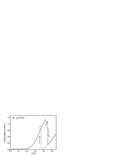

The bistability in TBRTD current-voltage characteristics can be explained by either the mathematical or physical arguments. If we consider the mathematical properties of the self-consistent Wigner-Poisson problem, we observe its nonlinearity. The solutions of the nonlinear problem are very sensitive to the initial conditions, therefore, they depend on the direction of the bias voltage change. Physical there are two orgins of bistability. First of them is the feedback between the charge accumulated in quantum wells and the flowing current [39, 40], and the second is a current oscillation [41]. The bias voltage V corresponds to one of the two bistability points in the current-voltage characteristics as it is shown in figure 7. We observe that both the potential energy and electron density are considerably different in the cases of increasing and decreasing bias voltage. The increasing bias causes that the electrons are localized in both the potential wells, however, the electron localization in the left quantum well is stronger (cf. solid curves in figure 7). The electron localization results from the formation of the quasi-bound states in both the potential well regions, which – at the resonant conditions – leads to the increase of the current. This type of behaviour is typical for asymmetric potential profile. On the contrary, the decreasing bias leads to the accumulation of electrons in the left spacer (near the left potential barrier). In this case, the electron density is almost zero within the potential wells which results in the considerable reduction of the maximal current [cf. figure 6(c)].

4 Conclusions and Summary
In the present paper, we have studied the transport properties of electrons in the triple-barrier resonant tunnelling diode. We have solved the Wigner-Poisson problem by the self-consistent procedure and determined the current-voltage characteristics for different gate voltage applied to the right potential well region. We have found the fairly large value (10) of the peak-to-valley ratio. The enlargement of the peak-to-valley ratio over that observed for the double-barrier resonant tunnelling diodes is caused by appearance of the linear regime within the negative differential resistance region that is produced by the join effect of the additional potential barrier and potential well. The additional potential barrier leads to the accumulation of electrons in the left spacer, while the second potential well leads to the formation of quasi-bound states in this potential well. For properly chosen nanodevice parameters the resonance conditions are satisfied for the quasi-bound states appearing in the three potential well regions, namely, the left spacer and two potential wells. This leads to a considerable increase of the resonant current peak.
We have also found interesting properties of the current-voltage characteristics of the TBRTD: the change of the negative differential resistance into the positive one (the occurrence of the notch in the regime of the linear dependence of the current on the bias voltage) and the bistability. We have explained these properties by analyzing the corresponding changes of the potential profile and electron density which are controlled by the gate potential. In the present study, we focus on the influence of the self-consistent Hartree potential on the transport properties of the TBRTD, therefore, we neglect the electron-phonon scattering. The bistable behaviour found in the current-voltage characteristics of the TBRTD requires a further study that should include the time dependence of the current.
In summary, the current-voltage characteristics of the triple-barrier resonant tunnelling diode shows a variety of interesting properties that can be effectively tuned by applying the gate voltage.
Acknowledgements
This paper has been supported by the Foundation for Polish Science MPD Programme co-financed by the EU European Regional Development Fund and the Polish Ministry of Science and Higher Education Programme ”International scientists mobility support”.
References
References
- [1] Baraff GA 1997 Phys. Rev. B 55 10745
- [2] Logan L R, Tang H H and Srinivasan G R 1991 Phys. Rev. B 43 6581
- [3] Barnaś J, Fuss A, Camley R E, Grünberg P and Zinn W 1990 Phys. Rev. B 42 8110
- [4] Sarker S K, Hu Y-K, Stanton C J and Wilkins J W 1987 Phys. Rev. B 35 9229
- [5] Wacker A, Jauho A-P, Rott S, Markus A, Binder P and Döhler G H 1999 Phys. Rev. Lett. 83 836
- [6] Harrison P 2001 Quantum Wells, Wires and Dots (John Wiley and Sons Ltd. Int. Edition) chapter 2
- [7] Datta S 1999 Electronic Transport in Mesoscopic Systems (Cambridge University Press) chapter 2
- [8] Landauer R 1970 Phil. Mag. 21 863
- [9] Li X-Qi and Yan J Yi 2007 Phys. Rev. B 75 075114
- [10] Iotti R C, Ciancio E and Rossi F 2005 Phys. Rev. B 72 125347
- [11] Bufler F and Schlösser J 1994 J. Phys.: Condens. Matter 6 7445
- [12] Mizuta H and Goodings C J 1991 J. Phys.: Condens. Matter 3 3739
- [13] Knezevic I and Ferry D 2004 Semicond. Sci. Technol. 19 S220
- [14] Cresti A, Farchioni R, Grosso G and Pastori Parravicini G 2003 Phys. Rev. B 68 075306
- [15] Datta S 2000 Superlattices Microstruct. 28 253
- [16] Lake R, Klimeck G, Bowen R Ch and Jovanovic D 1997 J. Appl. Phys. 81 7845
- [17] Nedjalkov M, Kosina H, Selberherr S, Ringhofer C and Ferry D K 2004 Phys. Rev. B 70 115319
- [18] Bertoni A, Bordone P, Brunetti R and Jacoboni C 1999 J. Phys.: Condens. Matter 11 5999
- [19] Bordone P, Pascoli M, Brunetti R, Bertoni A and Jacoboni C 1999 Phys. Rev. B 59 3060
- [20] Wigner E P 1932 Phys. Rev. 40 749
- [21] Hillery M, O’Connel R F, Scully M O and Wigner E P 1984 Phys. Rep. 106 121
- [22] Lee H-W 1995 Phys. Rep. 259 147
- [23] Kim K-Y and Lee B 2001 Phys. Rev. B 64 115304
- [24] Mains R K and Haddad G I 1980 J. Appl. Phys. 64 5041
- [25] Frensley W R 1987 Phys. Rev. B 36 1570
- [26] Kluksdahl N, Pötz W, Ravaioli U and Ferry D K 1987 Superlattices Microstruct. 3 41
- [27] Romo R, Villavicencio J and Garcia-Calderon G 2002 Phys. Rev. B 66 033108
- [28] Macks L D, Brown S A, Clark R G and Starrett R P 1996 Phys. Rev. B 54 4857
- [29] Wójcik P, Spisak B J, Wołoszyn M and Adamowski J 2008 Acta Phys. Pol. A 114 933
- [30] Fujita S 1966 Introduction to Non-Equilibrium Quantum Statistical Mechanics (London: Saunders) chapter 5
- [31] Ferry D K and Goodnick S M 1999 Transport in nanostructures (Cambridge University Press 1999) chapter 3
- [32] Kluksdahl N, Kriman A, Ferry D K and Ringhofer C 1989 Phys. Rev. B 39 7720
- [33] Frensley W R 1990 Rev. Mod. Phys. 62 745
- [34] Biegel B A and Plummer J D 1996 Phys. Rev. B 54 8070
- [35] Kim K-Y 2007 J. Appl. Phys. 102 113705
- [36] see e.g. Adamowski J, Bednarek S and Szafran B 2006 Handbook of Semiconductor Nanostructures and Nanodevices vol 1 ed Balandin A A and Wang K L (American Scientific Publishers) pp 389-452
- [37] Shewchuk T J, Chapin P C, Coleman P D, Kopp W, Fischer R and Morkoc H 1985 Appl. Phys. Lett. 46 508
- [38] e.g. Biegel B 1997 IEEE Transactions on Electron Devices 44 733
- [39] Goldman V J, Tsui D C and Cunningham J E 1987 Phys. Rev. Lett. 58 1256
- [40] Rahman M and Davis J H 1990 Semicond. Sci. Technol. 5 168
- [41] Sollner T C L G 1987 Phys. Rev. Lett. 59 14