Curvature Effects on Optical Response of Si nanocrystals in SiO2 having Interface Silicon Suboxides
Abstract
Several models of oxygenated and hydrogenated surfaces of Si quantum wells and Si nanocrystals of variable shapes have been constructed in order to assess curvature effects on energy gaps due to the three Si-suboxides. Si-suboxides in partially oxydized models of nanocrystals of spherical shapes (or quantum dots) are shown to reduce energy gaps compared to the hydrogenated nanocrystals, consistent with previous results in the literature. This trend is shown to be reversed when planar interfaces are formed in Si-NC inside SiO2 thin films, as in Si quantum wells. At planar interfaces (or surfaces) the electronic charge density is shown to become extended and to distribute among the Si-suboxides, thus generating along these planar interfaces extended, or delocalized, states. This delocalization of the electronic states then increase the energy gap compared to equivalent hydrogenated interfaces (or surfaces). Determination of geometric effects of curvature on the band gaps are based on density functional theory (DFT) using the real-space numerical approach implemented in the “Pseudopotential Algorithm for Real-Space Electronic Structure” (PARSEC) program. A method for measuring interface effects due to Si-suboxides in Si-NC in SiO2 is also suggested: by comparing photoluminescence (PL) between as-grown and annealed Si-NC samples. The DFT calculations suggest that blueshift of more than 0.2 eV of the PL should be observed in as-grown samples having Si-suboxides at their planar interfaces, in comparison to annealed samples above 950∘C that have fewer or no Si-suboxides once annealed, providing that the bulk of Si-NC remains unaltered.
pacs:
73.63.Hs, 73.63.Kv, 71.15.MbI Introduction
Silicon/SiO2 quantum wells (Si-QW) Lu as well as silicon nanocrystals in SiO2 (Si-NC)Thogersen ; Heitmann are examples of all-siliconCho ; Svrcek optoelectronic materials applicable to future generation high-efficiency photovoltaic multi-junctions tandem solar cells.HandbookPV Such devices are non-toxic and made of the two most abundant elements: silicon and oxygen. Both Si-QW and Si-NC structures constitute essentially artificial metastable forms of bulk-SiO2. However, quantum confinement of silicon in the form of Si-QW or Si-NC drastically modifies the electronic and optical properties of bulk-Si, and consequently, bulk-SiO2 as well. Quantum confinementRen transforms the indirect nature of the band gap of bulk-silicon Madelung into a direct band gap materialCarrier when the size of confinement of silicon is of the order of the wavelength of its electronic wavefunction (i.e., few nanometers), thus enhancing the photoluminescence (PL) of Si. Enhancements of PL due to quantum confinement in silicon were originally reported in porous-Si,Canham in Si-QW,Lu and in Si-NC .Linnros Another well known characteristic of quantum confinement is that the excitation energy increases with increased confinement. For instance, Si-QW are confined in one direction (1D-confinement) and the difference between the conduction band minimum (CBM) and valence band maximum (VBM), i.e., the band gap of the crystal, can vary from 1.5 eV for very thin wells (containing 2-3 monolayers of Si) down to 1.1 eV for larger wells. Si-NC, on the other hand, are further confined in the three directions (3D-confinement) and the difference between the lowest unoccupied molecular orbital (LUMO) and the highest occupied molecular orbital (HOMO) i.e., the HOMO-LUMO gap of the cluster, can vary from values just below the band gap of SiO2 (9 eV), when few silicon atoms form large enough clusters inside SiO2, down to the band gap of bulk-Si (1.1 eV). In practice, the reported HOMO-LUMO gaps in Si-NC are generally less than 4 eV.
The Si/SiO2 interface between the semiconductor Si and the dielectric medium SiO2 in Si-QW or Si-NC is the practical instrument for generating quantum confinement in physical device. In other words, the Si/SiO2 interface is inherent to the physics of Si quantum confinement and the influence of the atomic structure at the Si/SiO2 interface cannot be neglected. Determining the exact interface structure between Si and SiO2 is however a difficult task, mainly because SiO2 is amorphous. It is in part due to the large lattice mismatch between the two bulk materials: e.g., the lattice parameter of crystalline Si is =5.435 Å while that of SiO2 in the ideal -crystobalite phase is a=7.16 Å.CarrierDBMBOM For this reason SiO2 grown on crystalline-Si wafers is always amorphous. The planar SiO2/Si(100) interface structure has extensively been probed in the past especially for purposes of characterization of the metal-oxide semiconductor field-effect transistors (MOSFET) structure. In general, an SiO2/Si interface can be probed using high energy photons (e.g., 100 eV) that excite Si2p core electrons, i.e., using X-ray photoelectron spectroscopy (XPS).Fuggle XPS gives in general information on the chemical states between two different chemical environments (Si and SiO2 in this case) using binding energy and Auger electronic kinetic energy as parameters.Fuggle ; Mejias ; Thogersen The shift of the XPS spectrum in silicon-on-insulator (SOI) shows that planar SiO2/Si interfaces always contains three Si-suboxides, which are by definition three silicon atoms bonded to 1, 2, and 3 oxygens, respectively referred to as Si1+, Si2+, and Si3+. It has recently been shown, using XPS experiments as in the SOI, that the three Si-suboxides are also at the Si/SiO2 interfaces of Si-QWLuTay and Si-NC.Thogersen
Theoretical investigations that describe effects of oxygen on the band gap or the HOMO-LUMO gap in Si confined structures are more or less divided into two main groups: one group of investigations focusses on the structure of the planar Si/SiO2 interface, of particular interest in MOSFET or SOI, and in the Si/SiO2 QW (see Ref. Carrier, and references therein, or the Review on Si/SiO2 superlattices in Ref. Zheng, ). A second group of investigations focuses on oxygen passivation at the surface of spherical Si quantum dots (QD),Wolkin ; Vasiliev ; Puzder ; Nishida ; Koenig of particular interest for Si-NC in SiO2 thin films. This somewhat arbitrary division may be attributed to the difference in the treatment of boundary conditions (BC) in numerical simulations. Quantum wells are periodic systems, which is an ideal setting for Fourier basis (i.e., a plane wave set) used in general for simulation of crystals. Quantum dots are confined systems (with zero BC) which is an ideal setting for finite basis (e.g., gaussian set) used in general for simulations of molecules. Most of the results on the role of oxygen in Si confinement are thus usually confined to their respective geometries and rarely geometrical effects are juxtaposed. This article is intended to bridge this gap. It also resolves an apparent contradiction concerning the role of oxygen on band gaps for various interface topologies (planar or spherical), modeled using various BC.
The apparent contradiction on the role of oxygen in Si confined structures is the following: Surfaces of spherical Si-QD passivated with oxygen are reported to always reduce the HOMO-LUMO gap in comparison to equivalent hydrogen passivated surfaces.Puzder ; Vasiliev ; Wolkin This reduction of the energy gap is usually attributed to a larger localization of states at the oxygen sites of the surface.Puzder On the other hand, earlier results published by the author on Si-QW models containing the three Si-suboxides at the surface (or interface) of the well were shown to increase the band gap compared to equivalent hydrogenated QW models.Carrier This article first confirms the previous result Carrier using a different numerical framework described below. It also shows that the energy gap in Si-NC does not always decrease due to oxygen and that this gap variation depends also on the shape of the nanocrystal, especially if the nanocrystal has planar interfaces over just few nanometers, as shown below. Finally, a description of the mechanism leading to different variations of band gaps in Si-QW and Si-QD due to Si-suboxides is suggested. The mechanism is the following: Collective interactions between neighboring Si-suboxides is obviously increased at a planar surface compared to a large curvature nanocrystal. This increased interaction leads to extended, delocalized, electronic states at the surface, thus implying an increase of the band gap compared to similar hydrogenated surfaces. The interaction of neighboring Si-suboxides is less intense as the size of the Si-QD diminishes, due to simple curvature effects, which explains in part why oxygen atoms in Si-QD have reduced energy gaps compared to bare hydrogenated Si-QD (see Fig. 3 and discussion below). This collective effect that generates extended, or delocalized, electronic states at the interface or surface (see Fig. 4 and the discussion below) implies in particular that studying an individual Si-O atomic configuration or bond (e.g., a particular double-bond oxygen or bridge oxygen, or any particular Si-suboxide configuration, alone) in Si confined structures is indeed essential, but is not sufficient for explaining the whole process of energy gap variations due to surface or interface oxygen atoms.
II First-principles method
The Kohn-Sham equationKohnSham is resolved with the “Pseudopotential Algorithm for Real-Space Electronic Calculations” (PARSEC) program.PARSEC1 ; PARSEC2 ; PARSEC3 Using real-space instead of Fourier-space algorithms for solving the Kohn-Sham equation facilitates treatments and modifications of BC. It also facilitates comparisons of eigenenergies between different BC (periodic BC for the Si-QW and zero BC for the Si-QD) using identical numerical parameters. All pseudopotentials (PP) are constructed using the Troullier-Martins algorithm.TroullierMartins Silicon, oxygen, and hydrogen PP are constructed using 4, 6, and 1 valence electrons and the PP radii cutoffs are 2.782 a.u. (using local state), 1.452 a.u. (using local state), and 1.30 a.u. (using local state), respectively. Atomic relaxations are performed using the Broyden-Fletcher-Goldfarb-Shanno (BFGS) method.Nocedal Forces are less than 0.01Ry/a.u. (0.001 eV/Å) corresponding to energy gap errors less than 0.005 eV, tested on the model shown in Fig. 1. The real-space mesh is set to 0.45 a.u. for both periodic and zero BC which gives an error less than 0.00001 eV on the total energy per atom. The smallest supercell for the quantum wells has dimensions 7.675Å 7.675Å 24.621Å, which corresponds to a relatively small Brillouin zone (BZ). Tests on the model depicted in Fig. 2(c) using 442 k-points and using 221 k-points for the BZ sampling show that the latter constitutes a sufficiently fine k-point mesh. All structural relaxations and band gap evaluations have thus been performed using 221 k-points in the BZ. With these numerical parameters the size of the real-space Hamiltonian contains 2 millions elements in the largest model [Fig. 2(b)] and corresponds to finding 600 occupied eigenstates (2 electrons per levels, no spin-orbit interactions). Diagonalization of and Chebyshev filteringSaad are performed in parallel using Message Passing Interfaces (MPI) between 256 processors on an SGI Altix XE 1300 Linux Cluster or 128 processors on an IBM Bladecenter Linux cluster. For example, the largest distributed among 128 processors requires less than 400 Mb of memory per processors, a clear advantage of the real-space approach over other methods.
The exchange-correlation functional used throughout this work is the local density approximation (LDA).KohnSham The LDA is chosen for purposes of comparison with previous works.Carrier It is also chosen because the LDA band gap error in bulk-Si, caused by the self-interaction potentials, is well known and amounts to approximately -0.60 eV using the pseudopotential approach (the correction being slightly larger when using all-electrons methodsCarrierDBMBOM ). Moreover, the LDA band gap error seems to have little impacts on the band gap variations due to confinement in previous Si/SiO2 QW models, where good agreement with experiments on band gap variations were reported.MRS_Lockwood Nevertheless, rigidly shifting the energy gaps corresponds to assuming that the LDA energy gap error is independent of the chemical species in use. Such assumption might underestimates energy gap differences between SiOH and SiH models, based on the observation that the LDA band gap error of SiO2 in the -cristobalite phase is much larger than in silicon.CarrierAppSurf Therefore, the reported LDA blueshifts, below, constitute lower bounds of the full effects.
III Si Confinement Models
Two sets of models have been constructed in this work and are fully described in the next two paragraphs.
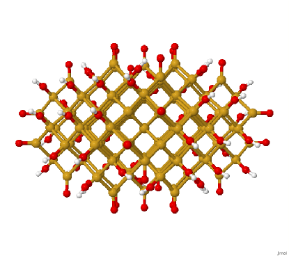
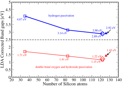
The first set is used for estimating general trends related to effects of shapes on the energy gaps using spherical, oblong, and disk-like Si-QD models. In these models the entire surface is uniformly passivated with hydrogen, or passivated with double-bond oxygen atoms and hydroxides. Three sizes of hydrogenated spherical Si-QD models have been constructed for evaluating general energy gap trends, with the number of [silicon, hydrogen] atoms being respectively [35, 36], [83, 72], and [122, 100] in each of the 3 sizes of models. Three other oxygenated spherical Si-QD models with [35, 30, 24], [83, 51, 30], and [122, 64, 28] [silicon, oxygen, hydrogen] atoms have also been constructed for comparison. They contain 6, 21, and 36 double-bond oxygens and 24, 30, and 28 hydroxides, respectively. The diameter (i.e., the largest distance between any two silicon atoms) of these dots are respectively about 1.09 nm, 1.38 nm, and 1.54 nm. Comparisons of shapes have been performed only on the largest dots. The hydrogenated oblong dot contains [122, 106] [silicon, hydrogen] atoms, a size directly comparable to the largest spherical dot. The oblong model has a shortest diameter of 1.09 nm which is also comparable to the diameter of the smallest spherical dots, and has a largest diameter of 2.46 nm. The oxygenated oblong dot contains [122, 68, 30] [silicon, oxygen, hydrogen] atoms. It corresponds to only 2 additional double-bond oxygens and 2 additional hydroxides than same size spherical dot described above. Finally, the hydrogenated disk-like dot model contains [126, 100] [silicon, hydrogen] atoms and its oxygenated disk-like dot counterpart contains [126, 74, 48] [silicon, oxygen, hydrogen] atoms. It corresponds to having 10 less double-bond oxygen atoms than its spherical counterpart and 20 more hydroxides, which are actually significant changes of bond types compared to all the other models of similar size. Nevertheless, this series of models is intended to provide general trends due to a uniform geometry of the structure. The diameter of the disk is about 1.92 nm and its thickness at the center is about 1.09 nm, which makes it again comparable to the smallest spherical dot containing 35 Si atoms. Each model is constructed so as to ensure uniformity of the structure. Fig. 1 depicts the oxygenated disk-like models. Results are further discussed in the next Section along with Fig. 3.
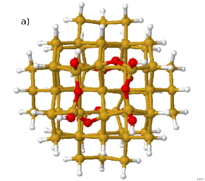
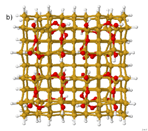
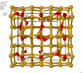
The second set of models are partially oxydized nanostructures containing the three Si-suboxides at the surface, as in XPS, and are derived from the superlattice models in Ref. Carrier, , depicted in Fig. 2(c). The purpose of this second set of models is to complement the first set. The first set was uniformly passivated but contained unrealistic oxygen bonds, while the second is oxydized only partially but contains realistic oxygen bonds and is intended to describe precise trends caused by a given structural configurations of Si-suboxides after modifying only the geometries. All oxygenated models are depicted in Fig. 2 and energy gaps are tabulated in Table 1 as further described in the next Section. Fig. 2(a) shows the spherical quantum dot. The diameter of the dot is 1.14 nm. It contains [66, 16, 56] [silicon, oxygen, hydrogen] atoms, with 4 of each of the Si1+, Si2+, and Si3+ suboxides. A hydrogenated spherical Si-QD models is constructed for comparisons of energy gaps (not depicted) and contains [66, 64] [silicon, hydrogen] atoms. Fig. 2(b) now shows the Si-NC that has two oxygenated planar surfaces of dimension 1.56 nm 1.56 nm separated by 1.14 nm, or 9 monolayers of Si. Notice that the thickness of the planar nanocrystal is identical to the diameter of the quantum dot of Fig. 2(a). It contains [178, 64, 104] [silicon, oxygen, hydrogen] atoms, with 16 of each of the Si1+, Si2+, and Si3+ suboxides. The two models in Fig. 2(a) and (b) were constructed starting from the periodic system depicted in Fig. 2(c), one by generating a sphere directly from the superlattice model, and the other by first doubling the cell in both – directions of the periodic supercell and then passivating all dangling bonds with hydrogen on the sides of the Si-well. All models in Fig. 2 have therefore identical structural atomic configurations for the Si-suboxides, and differ only by their geometries: (a) is a spherical quantum dot, (b) is a planar nanocrystal, and (c) is a crystalline superlattice. All atomic positions have been structurally relaxed in their respective geometries, using zero BC for the models in Fig. 2(a) and (b) and using periodic boundary conditions for the model in Fig. 2(c). Although bond lengths and bond angles surrounding the Si-suboxides vary slightly between geometries, those variations do not have a significant effect on the energy gaps reported below. For example, as stated above, the Si-QD model in Fig. 2(a) was constructed starting from the atomic positions of the Si-QW in Fig. 2(c) and such structural relaxation from the atomic positions of the QW suboxides towards these of the QD suboxides modify the LDA band gap by only 0.01 eV —from 2.35 eV to 2.36 eV— for a total energy variation per atom of 0.25 eV after the full structural relaxation is completed. It indicates that the energy gap variations inside the different geometries are independent of specific atomic structural relaxations. That is, the variations of the energy gaps reported in Table 1 are global topological effects and are not due to particular structural atomic configurations.
Notice that two general sets of models needed to be designed in this study for the reason that a Si-QD or Si-NC model containing the three Si-suboxides, as in the second set, and being uniformly distributed on an entire curved surface, as in the first set, has yet to be developed: such model has not been reported in the literature essentially because of its high complexity.
All atomic positions of the structurally relaxed models presented in this article are available from the author, upon request.
| Surface passivation | Si-H | Si-suboxides | difference |
|---|---|---|---|
| Si-QD | 3.17 | 2.96 | -0.21 |
| planar Si(100)-NC | 2.42 | 2.46 | +0.04 |
| Si(100) 2X1-QW | 1.53 | 1.82 | +0.29 |
| Si(100) 1X1-QW | 1.60 | - | +0.22 |
IV Results
Figure 3 shows the corrected LDA HOMO-LUMO gap results for the first set of models. Five observations stand out on this graph. (1) The quantum confinement effect is clearly noticeable: the energy gaps increase with increased confinements in both hydrogenated and oxygenated dots. (2) The presence of double-bond oxygens dramatically reduce the energy gaps compared to that of hydrogenated Si-QD of any shape. This was already noticed in previous works using spherical dots.Wolkin ; Puzder This significant drop of the energy gap due to double-bond oxygens is also observed in Si-QW. For instance, an Si-QW containing 9 monolayers (ML) of Si passivated with hydrogen has an LDA band gap of 1.00 eV (1.60 eV, with LDA correction) while the same well passivated with a double-bond oxygen gives an LDA band gap of 0.36 eV (0.96 eV, with LDA correction, i.e., below bulk-Si indirect band gap!). Although never observed to exist in silicates, the double-bond oxygen is however a useful surface and interface model for determining general trends on the variations of band gaps using simple uniform models chosen to have charge neutrality. (3) The energy gap variations with increased confinement of oxygenated spherical dots (red thin line in Fig. 3) is severely damped compared to that of hydrogenated dots (thick blue line). For instance, energy gaps of hydrogenated dots increase by 1.18 eV when dot size decreases from 122 to 35 Si atoms, while energy gaps of oxygenated dots increases by about half this value, 0.56 eV, for equivalent decrease in dot size. Smaller dots have larger curvature; larger curvature implies larger spacing between neighboring oxygens, which reduces interaction among neighboring oxygen atoms and consequently may increase localization of the electonic states. This suggests that a reduction of interaction between neighboring oxygen atoms at the surface further reduces the energy gap in comparison to hydrogenated Si-QD, assuming that increasing the size of dots from 1.09 nm to 1.54 nm does not significantly affect gap reduction due to size effects, i.e., the ratio of surface to bulk Si atoms [see also item (5) below where size effects are excluded]. (4) The shape of hydrogenated Si-QD does not radically affect the energy gaps. For instance, comparison in Fig. 3 of energy gaps for the hydrogenated spherical (square symbol), oblong (diamond symbol), and disk-like (filled-triangle symbol) Si-QD of similar size (122 or 126 silicon atoms) show that the trends along the thick blue line remain clearly unbroken. Moreover, the smallest diameter of the oblong and disk-like dots corresponds approximately to the diameter of the smallest spherical dot (1.09 nm), as described above, while energy gaps of the disk-like and the smallest spherical dots differ drastically (by 1.15 eV). This suggests that the smallest diameter of non-spherical quantum dots, which could have been viewed as the important confinement parameter for a given surface passivation, does not actually define the energy gap. It is rather the number of Si in the whole dot that defines the gap. Note that Ref. Justo, describes a similar trend concerning surface shapes in quantum wires. On the other hand, oxygenated Si-QD of different shapes show a slight variation of energy gaps with shapes, i.e., the trend along the thin red line is broken. These general trends indicate that shapes of Si-QD must be taken into account especially when considering oxygen passivation of surface and interface. (5) More precisely, disk-like oxygenated Si-QD show a noticeable increase of the band gap, by 0.2 eV above that of the other two models of similar sizes but different shapes. This suggests again that interactions between neighboring oxygen atoms might be the cause for an increased energy gap, because disk-like Si-QD have by construction two planar surfaces (see Fig. 1) where oxygen neighbors are closer and can interact more easily than in the other two geometries. Notice that point (5) is complementary to point (3), above. Point (3) showed that reducing the size of dots corresponds to reducing oxygen neighbor interactions due to curvature effects, thus reducing the energy gaps compared to that of equivalent hydrogenated Si-QD. Point (5) arrives at the same conclusion using equivalent dot sizes but with variable shapes. These qualitative effects on energy gap variations due to neighboring oxygen atoms based on these simplified uniformly passivated surface models are quantified next using the more realistic second set of models that contains the three types of Si-suboxides, as in XPS.
The second set of models was designed here in order to study effects of neighboring Si-suboxides at planar surfaces, using identical Si-suboxide atomic configurations for various geometries. By construction, the Si-suboxides at the center of the oxydized surfaces of the Si(100)-NC model in Fig. 2(b) can interact with each others as if they were located in the Si-QW of Fig. 2(c), while Si-suboxides at the periphery of that planar surface can only interact with Si-suboxides located towards the center of the plane as in the quantum dot of Fig. 2(a). In other words, the model in Fig. 2(b) is an hybrid between those of Fig. 2(a) and (c). Therefore, if neighboring Si-suboxides do affect the energy gap, as stated using the first set of models, then it is expected that the difference between the energy gaps of oxygenated and hydrogenated surfaces of the planar Si(100)-NC model should be intermediary to the equivalent differences of energy gaps from the Si-QD and from the Si-QW. It indeed is the case as given by Table 1: The HOMO-LUMO gap of the Si-QD with Si-suboxides is smaller than its hydrogenated counterpart, giving a difference of -0.21 eV. The band gap of Si-QW with Si-suboxides is larger than its hydrogenated counterpart, giving a difference of +0.22 eV, also in agreement with previous calculations using plane waves.Carrier Finally, the HOMO-LUMO gaps of the planar Si(100)-NC with or without Si-suboxides are relatively similar, a mere difference of +0.04 eV, and a value clearly in between that of the Si-QD and the Si-QW energy gaps. Notice that one possible explanation for smaller gap variations in the Si(100)-NC of Fig. 2(b) than in the Si-QD of Fig. 2(a) could be attributed to a size effect, where a much larger quantum dot would give smaller decrease of energy gaps due to oxygen than a smaller dot. However, it is found here that the HOMO-LUMO gap of the model in Fig. 2(b) does not show a decrease of the energy gap compared to its hydrogenated counterpart, as is usually the case in oxygenated Si-QD, but instead a slight increase. Furthermore, in the superlattice [Fig. 2(c)], which is basically the infinite extension of Fig. 2(b), the energy gap significantly increases due to oxygen. It thus means that there exist an additional mechanism not related to the size of the nanocrystal that does increase the energy gap in the presence of Si-suboxides, at least at planar surfaces. The fact that the energy gap increases due to oxygen was interpreted using the first set of models above by an enhanced interaction between neighboring Si-suboxides at the planar surfaces of the disk-like dot, that further delocalizes electronic states and thus increases the energy gap. This interpretation is further established next by plotting the charge density along the plane of the Si-suboxides in the Si(100)-NC model of Fig. 2(b).
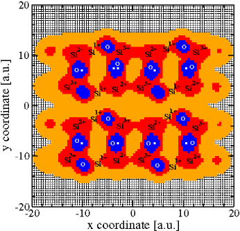
It is clear from this study, and from previous publications, that energy gaps in spherical Si-QD as in Fig. 2(a) decrease due to an increased localization of the electronic states caused by oxygen atoms. Any oxygen atom tends to accumulate charge because of its large electronegativity, equal to 3.44. Now, the effect of (de)localization due to Si-suboxides at the planar surface can be established by depicting the charge density along the plane formed by the Si-suboxides in the model of Fig. 2(b), as shown in Fig. 4. The first observation from the Figure is that oxygen indeed tend to accumulate charge (i.e., the darkest blue regions are on the oxygen sites in Fig. 4 and are the most intense charge densities), as expected. Most importantly, in addition to these peaks of densities located onto the oxygen sites, the charge distribution surrounding the oxygen charge density peaks is also significant and remains relatively evenly distributed around those peaks, especially at the Si3+ and the Si2+ (the dark red regions in Fig. 4). It thus suggests that multiplying interactions among Si-suboxides, i.e., when there are sufficiently enough Si-suboxides and when they are close enough and are bridging each others, then Si-suboxides act as collective entities and tend to delocalize the electronic states, from the oxygen sites where the charge remains largely concentrated towards the silicon suboxide atoms where the charge becomes relatively evenly distributed. This slight delocalization of the electronic states then induces an increase of the band gap compared to an equivalent hydrogenated surface. Both Si3+ and the Si2+ seem to be instrumental to the generation of extended states along that nanosurface. Inspection of the charge distribution (darker red areas) in the Figure shows that this distribution is more intense at the Si3+ and Si2+ sites then onto the Si1+. It can be attributed to the fact that, on average (since SiO2 is amorphous in real devices), Si3+ suboxides have more oxygens bridging other silicons than the Si2+, and furthermore than any of the Si1+ suboxides.
V Conclusions
This result concerning the relation between energy gap and planar surface of few nanometers in diameter has interesting consequences for measurements of energy gaps in Si-NC, when planar surfaces are observed at the nano-scale. For instance, recent photographs of high resolution transmision electron spectroscopy (HRTEM) show that such nanometer-long planar surfaces can form.Thogersen This first-principles calculation suggests that planar surfaces in Si-NC may contribute at least 0.2 eV to the overall energy gap values in the PL. Such blueshift due to interface Si-suboxides may be measurable by comparing PL between as-grown samples and samples annealed at temperatures at which Si-suboxides are reported to vanish (above 950∘C),Thogersen assuming no significant alterations to the bulks of the nanocrystals during annealing.
In summary, several models of oxygenated and hydrogenated surfaces of Si confined quantum wells and nanocrystals of variable shapes have been constructed in order to determine interface curvature effects on energy gaps due to Si-suboxides. Si-suboxides in quantum dots of spherical shapes are shown to reduce band gaps compared to hydrogenated dots, consistent with previous published results in the literature. However, this trend is shown to be reversed when planar surfaces are formed, such as in Si-NC inside SiO2 thin films, or in Si quantum wells. At planar surfaces of few nanometers in diameter collective interactions among Si-suboxides are enhanced, especially among the Si3+ and Si2+, which induces a delocalization of the electronic states and thus increases the band gap compared to equivalent hydrogenated surfaces.
Hybrid density functionals are to be considered in the future for determining blueshifts closer to experimental values. Models of Si-NC with entire surfaces passivated by the three Si-suboxides, as well as - dopants, are under development by the author.
Acknowledgements This work is supported by NSF/DMR-0551195 through the PARSEC project. The author wants to thank Prof. Yousef Saad for providing resources and discussions, Shuxia Zhang from the Minnesota Supercomputing Institute for her assistance with optimizing the PARSEC code and the two referees for their fruitful comments.
References
- (1) Z. H. Lu, D. J. Lockwood, J.-M. Baribeau, Nature 378, 258 (1995).
- (2) A. Thogersen, S. Diplas, J. Mayandi, T. Finstad, A. Olsen, J. F. Watts, M. Mitone, and Y. Bando, J. Appl. Phys. 103, 024308 (2006).
- (3) J. Heitmann, F. Müller, M. Zacharias, and U. Gösele, Advanced Materials 17, 795 (2005).
- (4) E.-C. Cho, M. A. Green, G. Conibeer, D. Song, Y.-H. Cho, G. Scardera, S. Huang, S. Park, X. J. Hao, Y. Huang, and L. V. Dao, Adv. OptoElectronics, 2007, 69578 (2007).
- (5) V. Švrček, A. Slaoui, and J.-C. Muller, Thin Solid Films 451-452, 384 (2004).
- (6) Handbook of Photovoltaic Science and Engineering, ed. by A. Luque and S. Hegedus (Wiley, Hoboken, 2003)
- (7) S. Y. Ren, Electronic States in Crystals of Finite Size, Quantum Confinement of Bloch Waves (Springer, Berlin, 2006).
- (8) O. Madelung, Semiconductors: data Handbook (Springer-Verlag, Berlin, 2004).
- (9) P. Carrier, L. J. Lewis, and M. W. C. Dharma-wardana, Phys. Rev. B 65, 165339 (2002)
- (10) L. T. Canham, Appl. Phys. Lett. 57, 1046 (1990).
- (11) J. Linnros, N. Lalic, A. Galeckas, and V. Grivickas, J. Appl. Phys. 86, 6128 (1999).
- (12) P. Carrier, L. J. Lewis, and M. W. C. Dharma-wardana, Phys. Rev. B 64, 195330 (2001)
- (13) J.C. Fuggle, in Unoccupied Electronic States, Vol. 69 of Topics in Applied Physics, edited by J.C. Fuggle and J.E. Inglesfield, (Springer-Verlag, Berlin, 1992).
- (14) J. A. Mejías, V. M. Jiménez, G. Lassaletta, A. Fernández, J. P. Esponós, and A. R., González-Elipe, J. Phys. Chem. 100, 16255 (1996).
- (15) Z. H. Lu, S. P. Tay, T. Miller, and T.-C. Chiang, J. Appl. Phys. 77, 4110 (1995).
- (16) T. Zheng and Z. Li, Superlattices and Microstructures 37, 227 (2005).
- (17) M. V. Wolkin, J. Jorne, P. M. Fauchet, G. Allan, and C. Delerue, Phys. Rev. Lett. 82, 197 (1999).
- (18) I. Vasiliev, J. R. Chelikowsky, and R. M. Martin, Phys. Rev. B 65, 121302 (2002).
- (19) A. Puzder, A. J. Williamson, J. C. Grossman, and G. Galli, J. Chem. Phys. 117, 6721 (2002).
- (20) M. Nishida, Phys. Lett. A 323, 449 (2004).
- (21) D. König, J. Ruud, M. A. Green, and G. Conibeer, P hys. Rev. B 78, 035339 (2008).
- (22) P. Hohenberg and W. Kohn, Phys. Rev. B136, B864 (1964); W. Kohn and L. J. Sham, Phys. Rev. A140, A1133 (1965).
- (23) J. R. Chelikowsky, N. Troullier, and Y. Saad, Phys. Rev. Lett. 72, 1240 (1994).
- (24) J. R. Chelikowsky, J. Phys. D 33, R33 (2000).
- (25) M. M. G. Alemany, M. Jain, L. Kronik, and J. R. Chelikowsky, Phys. Rev. B 69, 075101 (2004).
- (26) N. Troullier and J. L. Martins, Phys. Rev. B 43, 1993 (1991).
- (27) C. Zhu, R. H. Byrd, and J. Nocedal, ACM Trans. Math. Soft. 23, 550 (1997).
- (28) Y. Zhou, Y. Saad, M. L. Tiago, J. R. Chelikowsky, J. Comp. Phys. 219 172 (2006).
- (29) D. J. Lockwood, M. W. C. Dharma-wardana, Z. H. Lu, D. H. Grozea, P. Carrier, and L. J. Lewis, Mat. Res. Soc. Symp. Proc. 737, F1.1 (2001).
- (30) P. Carrier, L. J. Lewis, and M. W. C. Dharma-wardana, Appl. Surf. Sci. 212-213, 826 (2003).
- (31) J. F. Justo, R. D. Menezes, and L. V. C. Assali, Phys. Rev. B 75, 045303 (2007).
- (32) A. Pasquarello, M. S. Hybertsen, R. Car., Appl. Phys. Lett. 68, 625 (1996)