Charge oscillation-induced light transmission through subwavelength slits and holes
Abstract
We present a concrete picture of spoof surface plasmons (SSPs) combined with cavity resonance to clarify the basic mechanism underlying extraordinary light transmission through metal films with subwavelength slits or holes. This picture may indicate a general mechanism of metallic nanostructure optics: When light is incident on a non-planar conducting surface, the free electrons cannot move homogeneously in response to the incident electric field, i.e., their movement can be impeded at the rough parts, forming inhomogeneous charge distributions. The oscillating charges/dipoles then emit photons (similar to Thomson scattering of x rays by oscillating electrons), and the interference between the photons may give rise to anomalous transmission, reflection or scattering.
pacs:
42.25.Bs, 42.79.Dj, 78.67.-n, 84.40.AzSince the discovery of extraordinary light transmission through metal films perforated by subwavelength hole arrays r1 , tremendous theoretical and experimental work has been carried out to understand the underlying physics. Several mechanisms, particularly surface plasmons (SPs), have been proposed as the possible origins r2 ; r3 ; r4 ; r5 ; r6 ; r7 ; r8 . However, no universal understanding has been reached to date. Here based on first-principle calculations, we present a charge oscillation-induced light emission mechanism, which gives the origin of enhanced transmission in subwavelength systems and may also shed light on the fundamental of interactions between light and metallic nanostructures.
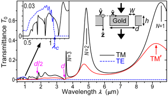
In non-magnetic media, the electric and magnetic fields are coupled by Maxwell’s equations and (, the wavelength in vacuum, and the effective permittivity). For varying ) (i.e., ), the divergence of the second equation generally gives , where is the charge density. Consider in Fig. 1 the free-standing one-dimensional (1D) gold grating illuminated by a plane wave, where Maxwell’s equations can be solved by the rigorous coupled-wave analysis (RCWA), a first-principle method r9 . For simplicity, we only discuss normal incidence in this Letter. Figure 1 shows the zero-order transmittance () spectra of both TM () r4 ; r5 and TE () waves r10 . Here RCWA correctly reveals the cutoff wavelength , above which transmission of TE waves is forbidden. The reason is that TE waves in the slit approximately take the waveguide modes ( being integers) r11 , where for , all the modes are evanescent. The drastic difference between the TE and TM spectra stems from the fact that TE waves satisfy while TM waves may induce electric charge oscillation ( the frequency), where .
For TM polarization, the vertical component of the electric field (invariant with ) has abrupt discontinuity across the surfaces at and , from which one obtains the surface charge density . In Fig. 2(a), the calculated profile correctly shows that charges only exist on the metal surface [ for ], and the charges tend to accumulate at the metal corners. At resonant wavelengths, , i.e., the charge patterns on the two surfaces are nearly the same, but they have opposite signs for odd resonant numbers (defined below). The bulk charge density is given by . In Fig. 2(b), the curve calculated from the internal eigenmodes reveals that there is a strong peak exactly centered at each slit wall, or (plus any multiple of ). When sufficient diffraction orders (1601 orders in Fig. 2) are retained in RCWA, approaches a delta function across [see Inset of Fig. 2(b)], i.e. charges inside the grating also appear as surface charges on the walls.
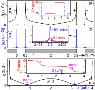
The profile [] plotted in Fig. 2(c) shows that in the central range the charge density on the wall is nearly a standing wave (with wavevector ). This indicates that the electric field in the slit is also a standing wave r12 ; r13 consisting of a forward wave and a backward wave in Fig. 3. Note that increases sharply when in Figs. 2(c). Mathematically, the charge density at each corner consists of both and . Since they are always in phase, these two contributions are superimposed constructively. This makes the total charge densities at the corners much higher than in other regions, which is a typical edge effect. Consequently, there exist two large oscillating dipoles at the two ends of the slit.
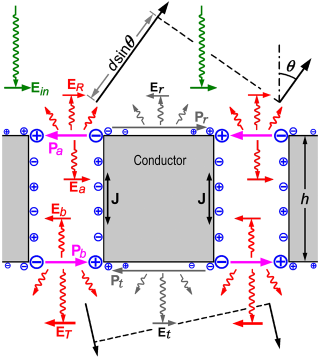
Now we may obtain a clear picture about the light scattering process. As shown in Fig. 3, the incident electric field drives (mainly) free electrons on the metal surface to move, but the movement is blocked at one corner of the metal, resulting in accumulation of electrons there. Meanwhile, extra positive charges appear at the other corner since some of the electrons have moved away. Thus, two dipoles and are formed. Since they oscillate with the incident wave, these dipoles act as light sources emitting new wavelets (photons), which form scattered waves (Thomson scattering). If we consider each period of the array as an overall scattering unit, the wavelets emitted from two adjacent units have a path difference along an arbitrary direction . Note that for a subwavelength slit array with , we have , so the phase difference can never reach . This means that the oblique wavelets always tend to cancel each other out in the far fields (destructive interference, similar to the absence of x-ray diffraction at non-Bragg angles). Thus, they form evanescent waves near the surface. Mathematically, these evanescent waves can be expressed as , where ( being integers) and (note that for ) r9 .
One may prove that for any wavelength , the charge patterns on the upper surface are always the same as that in Fig. 2(a) except that the peak heights vary with . Therefore, the period of the charge density wave always equals the lattice constant and generally does not satisfy the dispersion relation of a classical SP (CSP) r14 at all ( the conductor’s permittivity and the wavevector of the CSP). However, the evanescent waves are indeed surface-bound modes with their strengths decaying exponentially along . So they are spoof SPs (SSPs) r15 , but their formation is the result of charge oscillation-induced light emission and destructive interference. The SSP model has been conceptually proposed by Pendry et al. r3 (also see r16 ). Here we provide a concrete picture illustrating its origin.
The wavelets propagating along the backward direction () are always in phase (the path difference is zero). Therefore, the back reflected wave is not evanescent but a propagating mode. However, since and always have opposite directions, they tend to offset each other, thus reducing the overall back reflection.
In Fig. 3, dipole also emits a wavelet inside the slit. Similarly, electrons on the slit walls also move in response to the electric field in the slit (represented by the current ). Then the charge movement is disrupted again at the exit edges, giving rise to another large dipole . Through this tunneling process, the charge patterns on the upper surface are duplicated on the lower surface. Oblique wavelets emitted from these duplicated light sources then form SSPs again below the grating. The sub-wavelets and along the forward direction form the zero-order transmitted wave. Overall, the grating only emits two propagating modes, the reflected and transmitted waves, that share the incident energy, while all the other modes are SSPs.
The oscillating dipole can give a strong feedback to the upper surface by emitting a wavelet propagating upward. If is not in phase with (and ) at , it suppresses the strengths of and . Then , which includes specular reflection from the metal surface, becomes dominant, leading to strong backward reflection. The weakened meanwhile reduces . However, if is in phase with at , it enhances . The enhanced subsequently strengthens , , , and so on. Then a Fabry-Perot-like resonant state is formed with the strengths of all the dipoles and wavelets maximized. Under this condition, is largely offset by in the far-field regions, leading to minimized backward reflection. Below the grating, wavelet also partly offsets , but can be much larger than (unlike , does not include any specular reflection). Therefore, when is maximized, it maximizes . The resonant wavelength is always slightly longer than , the ideal Fabry-Perot wavelength, where is the resonant number (number of the standing wave nodes). Although the Fabry-Perot-like resonance has been recognized before r4 ; r5 ; r12 ; r13 ; r17 ; r18 , here we explictily illustrated its origin. Particularly, Figure 3 shows that it is dipoles and that act as the two “reflecting planes” required to form a vertical resonator r13 .
Note that when , some of the oblique waves satisfying become propagating diffracted waves (i.e., they are no longer SSP modes). The sharing of the incident energy by these diffracted waves significantly reduces (and backward reflection). This explains the much lower transmittance in the range in Fig. 1.
Light scattering from a 2D hole array has a similar picture. The incident electric field drives electrons on the upper surface to oscillate. The charge movement is blocked at the hole edges, giving rise to oscillating dipoles at the entrance openings. Thus, the holes act as a 2D array of light sources. For a subwavelength lattice with (Fig. 4), the phase difference between wavelets emitting from adjacent holes again is less than along any oblique directions. So these wavelets form SSPs above the film except that the wavelets along constitute a non-evanescent reflected wave (which offsets specular backward reflection). Meanwhile, the charge patterns are tunneled onto the lower surface due to the charge movement on the hole walls. Consequently, a similar set of SSPs and a forward transmitted wave are formed below the film.
However, 2D holes have a different tunneling mechanism. Consider the rectangular hole (a unit cell of an array) in Fig. 4. Except for the wave distortions near the ends, the electric fields in the hole roughly take the waveguide modes. For subwavelength holes, the basic 2D TE1,0 modes dominate r3 ; r11 . When , the modes in the hole are evanescent and approximately take the forms and , where r13 . drives charges on the walls to move/oscillate, but the charge density decays with decaying toward due to the waveguide restriction. Nevertheless, the sharp discontinuity of the charge movements at the exit end can still cause significant accumulation of charges there, giving rise to a relatively large dipole , provided that is adequately small. Since and no longer have position-dependent phase factors, they are always in phase with each other and the incident wave, and they always resonate as the feedback is always constructive. But the strengths of the dipoles and wavelets decrease with increasing due to the decaying effect. For fixed and in the absence of diffraction effects, the transmittance would increase monotonically with decreasing toward ( decreasing). However, when , diffracted waves emerge, which reduces the zero-order transmittance in the short-wavelength range. Therefore, strongest transmission must occur for , the non-diffraction range, but meanwhile should still be close to so that the damping coefficient is sufficiently small.
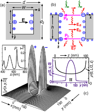
This picture agrees very well with the measured transmission spectra in the literature, and our finite-difference time-domain (FDTD) computations have unambiguously proved it. Figure 4(c) shows the calculated charge distribution on a free-standing silver film with a hole array, where the charges again exist mainly on the two walls (perpendicular to the charge movement direction). The residual charges in other regions are surface charges and they disappear for . (Here note that FDTD gives the overall charge densities.) The shape of the [] profile is independent of , but the maximum density changes with in inset II. Here our calculations indeed reveal the two large dipoles at the two openings of the hole (also see r19 for the single-hole case).
The above illustrations may indicate a general Thomson scattering mechanism of metallic nanostructures similar to x-ray scattering by oscillating electrons. That is, free electrons on a non-planar conducting surface cannot move homogeneously in response to the incident wave, thus forming inhomogeneous charge distributions. The oscillating charges then emit wavelets, and the interference between the wavelets may give rise to anomalous light scattering. The basic requirement here is free electrons, so this mechanism can explain scattering from various conducting nanostructures, including perfect conductors and conductors with Re (see the TM′ curve in Fig. 1 and the experiments and simulations of tungsten hole arrays with positive Re in r8 ; r20 ). It is also applicable to non-periodic structures. For example, Figure 3 indicates that an isolated slit (or hole) can still be a single light source emitting divergent light. If the slit is surrounded by grooves (in which the cavity resonance may be different though), the grooves provide additional light sources that suppress the oblique wavelets (forming SSPs). Meanwhile, wavelets emitted from the grooves along the backward direction offset specular reflection. Thus, transmission is enhanced. If grooves also exist on the exit surface, they again suppress oblique wavelets so that a collimated zero-order transmitted beam can be achieved r2 . As another example, it is known that when a nanowire is illuminated by a TM wave at one end, light can be “transferred” to the other end r21 ; r22 . The common explanation is that light is transferred by CSPs on the wire, but the dispersion trend in r21 is quite different from that of CSPs. Based on our mechanism, the incident wave causes inhomogeneous charges at the illuminated end that tend to propagate away due to the charge-netural tendency. This is similar to normal electricitiy transmission over metallic wires. The charge movement is then discontinued at the other end, leading to charge accumulation and oscillation that emit new light. The electrons can be bounced back, resulting in a Fabry-Perot-like charge pattern (that obviously do not need to obey the CSP principle). Here high conductivity can enhance the transfer efficiency, which is opposite to the CSP prediction that (nearly) perfect conductors do not support CSPs. Overall, our mechanism reveals the fundamental of metallic nanostructure optics.
X.R.H is grateful to A. T. Macrander and S. K. Gray for invaluable suggestions and discussions. This work was supported by the U.S. Department of Energy, Office of Science, Office of Basic Energy Sciences, under Contract No. DE-AC02-06CH11357, and by the National Nature Science Foundation of China (10625417, 50672035, 10021001) and the Ministry of Science and Technology of China (the State Key Program for Basic Research, 2004CB619005, 2006CB921804).
References
- (1) T.W. Ebbesen et al., Nature (London) 391, 667 (1998).
- (2) W.L. Barnes, A. Dereux, and T.W. Ebbesen, Nature (London) 424, 824 (2003); C. Genet and T. W. Ebbesen, ibid. 445, 39 (2007).
- (3) J.B. Pendry, L. Martín-Moreno, and F.J. Garcia-Vidal, Science 305, 847 (2004).
- (4) Q. Cao and P. Lalanne, Phys. Rev. Lett. 88, 057403 (2002).
- (5) J.A. Porto, F.J. García-Vidal, and J.B. Pendry, Phys. Rev. Lett. 83, 2845 (1999).
- (6) M.M. Treacy, Phys. Rev. B 66, 195105 (2002).
- (7) A.P. Hibbins, B.R. Evans, and J.R. Sambles, Science 308, 670 (2005).
- (8) H.J. Lezec and T. Thio, Opt. Express 12, 3629 (2004).
- (9) M.G. Moharam et al., J. Opt. Soc. Am. A 12, 1068 (1995); P. Lalanne and G.M. Morris, ibid. 13, 779 (1996).
- (10) Permittivities from Handbook of Optical Constants and Solids, edited by E.D. Palik (Academic, Orlando, 1985).
- (11) K. Kawano and T. Kitoh, Introduction to Optical Wave-guide Analysis (John Wiley & Sons, New York, 2001).
- (12) E. Popov et al., Phys. Rev. B 62, 16100 (2000).
- (13) A.P. Hibbins, M.J. Lockyear, and J.R. Sambles, J. Appl. Phys. 99, 1124903 (2006).
- (14) J.R. Sambles, G.W. Bradbery, and F. Yang, Contemp. Phys. 32, 173 (1991).
- (15) The period of a CSP also satisfies [for finite with ]. A sinusoidal CSP on a planar surface is a true surface mode since along the normal direction, the two sub-wavelets emitted from a period are symmetric so that they are always cancelled out. CSP excitation depends on the intrinsic dielectric properties of the metal while SSPs corresponds to a geometrical effect.
- (16) A.P. Hibbins et al., Phys. Rev. Lett. 96, 073904 (2006).
- (17) H.E. Went et al., Appl. Phys. Lett. 77, 2789 (2000).
- (18) S.V. Kukhlevsky et al., Phys. Rev. B 72, 165421 (2005).
- (19) F.J. García-Vidal et al., Phys. Rev. Lett. 95, 103901 (2005).
- (20) M. Sarrazin and J. Vigneron, Phys. Rev. E 68, 016603 (2003).
- (21) K. Wang and D.M. Mittleman, Phys. Rev. Lett. 96, 157401 (2006).
- (22) H. Ditlbacher et al., Phys. Rev. Lett. 95, 257403 (2005).