Domain boundary formation in helical multishell gold nanowire
Abstract
Helical multishell gold nanowire is studied theoretically for the formation mechanism of helical domain boundary. Nanowires with the wire length of more than 10 nm are relaxed by quantum mechanical molecular dynamics simulation with tight-binding form Hamiltonian. In results, non-helical nanowires are transformed into helical ones with the formation of atom pair defects at domain boundary, where the defective atom pair is moved from an inner shell. Analysis of local electronic structure shows a competitive feature of the energy gain of reconstruction on wire surface and the energy loss of the defect formation. A simple energy scaling theory gives a general discussion of domain boundary formation.
pacs:
64.70.Nd, 71.15.Pd, 73.22.-f1 Introduction
Nanometer scale material forms exotic structures and it is crucial to understand and control their formation mechanism, so as to establish the foundation of nano electronics. Helical multishell gold nanowire [1, 2] is one of exotic metal nanostructures [3] and has characteristic multishell configurations with ‘magic numbers’. The helical wires were synthesized by focusing electron beam on thin film. [4] The wire axis is in the [110] direction of the original FCC structure and the outermost shell is a folded (111)-type (hexagonal) atomic sheet with helicity. A single shell helical structure was synthesized later. [5] The transport property was studied theoretically [6] and experimentally [7]. Platinum nanowires were also synthesized with the same type of helicity. [8]
The observed multishell structures of the helical gold nanowires [1] are denoted by the numbers of atoms in each shell and are classified into 7-1, 11-4, 13-6, 14-7-1, 15-8-1 structures. For example, a ‘14-7-1 nanowire’ is a nanowire with three shells and the outer, middle and inner shells have fourteen, seven and one atom(s) in the section view, respectively. These numbers are called ‘magic numbers’, since the difference of the numbers between the outermost and next outermost shells is seven, except the cases of the 7-1 structure.
Theoretical investigations were carried out for the helical nanowire structures [9, 10, 11, 12, 14, 13, 15, 16, 17] and, among them, a recent theory [15, 18] explains the observed multishell configuration with ‘magic numbers’ systematically. The theory was proposed as a two-stage formation model of helical multishell gold nanowires and the model was confirmed by quantum mechanical molecular dynamics simulations for gold and copper with tight-binding form Hamiltonians. The simulation shows the energy relaxation process from non-helical structures into helical ones. The analysis of electronic structure concluded that the origin of the helicity comes from the intrinsic nature of non-spherical electrons and a (111)-type (hexagonal) surface structure is energetically favorable for electrons in sheet structure. The above mechanism gives a general understanding among (i) the appearance of helical nanowire structures of gold and platinum and (ii) the fact that reconstructed equilibrium surfaces of FCC 5 metals, gold platinum and iridium, prefer (111)-type structures. [19, 20, 21, 22, 23, 24, 25] After the theory paper, [15] several related simulations were carried out for formation of helical gold nanowire within tight-binding form Hamiltonian. [16, 17]
The present paper investigates the formation of helical domain boundary on wire surface, where the fundamental picture and simulation method are shared with the previous theory paper. [15] In general, a defect should be introduced at domain boundary in the formation process of a helical domain from non-helical one. The information of domain boundary is missing in the previous paper, since the simulated structures are short isolated wires of which wire length is less than 3 nm. In the resultant helical nanowires, the domain boundaries are located in the wire ends that are terminated artificially. In the present paper, simulations are carried out with longer wires, longer than 10 nm, and reveal a possible defect induced mechanism for forming helical domain boundary.
This paper is organized as follows; Section 2 describes the methodology and result of the simulation. Section 3 focuses on the analysis of the results, particularly on the energy per atom and the local density of states (LDOS). In Sec. 4, a simple energy scaling theory with respect to the wire length of helical domain is constructed for a general mechanism of domain boundary formation. Finally, the summary and future aspects are given in Sec. 5.
2 Simulation
The formation process of the helical wires is realized by quantum mechanical molecular dynamics simulation as a structure relaxation with thermal fluctuation. The temperature was set to be 600 K, lower than the melting temperature (1337K). The simulation code used here has the name of ‘ELSES’ (=Extra-Large-Scale Electronic Structure calculations). [26, 27, 28, 29, 30, 31, 32, 33, 15, 16, 34, 35]. The simulation was realized with a tight-binding form Hamiltonian [36, 37, 38], which was used for gold nanowire. [40, 41, 39, 15, 16, 17] The Hamiltonian form contains several parameters and they are determined to represent electronic structures of bulk solids, surfaces, stacking faults and point defects. One iteration step corresponds to fs. Eigen state calculation for electronic structure is carried out at each iteration step. The boundary condition is imposed by fixing the mass center of the wire end layers. [15] The computational time with 608 atoms is typically nine minutes per one iteration step, when a workstation with four dual-core Opteron(TM) processors was used.
We should say that the present simulation is different from experiment in several points. For example, the simulated time is quite short, 7-9 ps, owing to the practical limit of computational resource. Therefore, the simulation result should be understood so that it captures an intrinsic energetical mechanism of the real process.
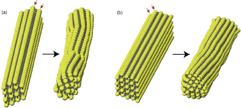
The resultant nanowires are shown in Fig. 1 for the (a) 11-4 and (b) 15-8-1 structures and contain multiple helical domains on wire surface with well-defined domain boundary, unlike the smaller samples in the previous paper. [15] The initial structures are parts of ideal FCC structure and are the same as those in the previous paper, except their wire length. The wire lengh of these nanowires is approximately 12 nm or is 40 or 42 unit layers for the 11-4 and 15-8-1 structures, respectively. Here a unit layer of a [110] nanowire consists of two successive atom layers. At the initial structures, the wire surface consists of (111)-type (hexagonal) and (001)-type (square) areas. The latter area consists of two atom rows that are indicated by the two parallel arrows in Fig. 1. Defect structures appear on wire surface as helical domain boundary. Hereafter the domain boundary formation of the 11-4 structure will be focused on.
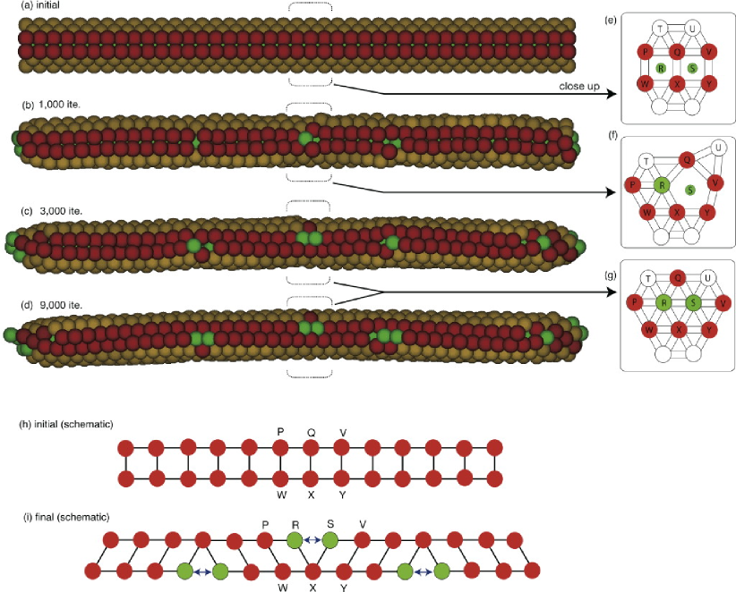
Figure 2 shows several snapshots of sideview for the 11-4 case, where the atoms are distinguished by color, so as to clarify the transformation process. Red atoms are those initially placed on the (001)-type surface area and green atoms are those initially placed in the inner shell region. The other atoms are those initially placed on the (111)-type surface area. The central region indicated by broken lines at Fig. 2(a)-(d) is sketched in Fig. 2(e) (f) and (g). Figure 2(e) and (f) capture the structures of Fig. 2(a) and Fig. 2(b), respectively and Fig. 2 (g) captures the structure of Fig. 2(c) or Fig. 2(d). At the initial structure, Fig. 2(e), the ‘red’ atoms, marked as and , form a square lattice on wire surface and the ‘green’ atoms, marked as and , are placed in the inner shell. At the final snapshot, Fig. 2(g), the two ‘green’ atoms and , are moved from the inner shell into the wire surface, which form a helical domain boundary. They are inserted between the atoms and , while the atom is moved into an upper area between the atoms and . As result, the surface reconstruction occurs, from the (001)-type (square) lattice into the (111)-type (hexagonal) one, and introduces the helical domains with domain boundaries.
As a remarkable tendency of the entire sample, surface defects at domain boundaries appear typically as pairs of ‘green’ atoms, as illustrated in Fig. 2(h) and (i). The central atom-pair defect, the pair of the atom and , appears, because the shear-like deformation on the (001)-type lattice occurs in the opposite shear directions between the left and right areas of the defect, as indicated by a blue arrow in Fig. 2(i).
3 Analysis of local electronic structure
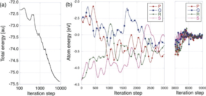
The transformation process from the non-helical wire into the helical one occurs with energy gain, according to the change of the total energy shown in Fig. 3(a).
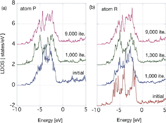
The change of the atom energy, energy of each atom, is plotted in Fig. 3(b) for the selected atoms , , and , that are indicated in Figs. 2 (e), (f) and (g). Figure 4(a) shows the LDOS of the atom at the initial structure and the 1,000-th and 9,000-th steps. Figure 4(b) shows the LDOS of the atom at the initial structure and the 1,000-th, 1,300-th and 9,000-th steps. In Fig. 4, the origin of the vertical axis is shifted among the snapshots and the origin of the horizontal axis is set to the Fermi level for each snapshot. Since the values of the Fermi level are different only about or within 0.1 eV among the snapshots, the difference in the Fermi level is negligible in the energy scale of the graphs. Since the atoms is placed in the inner shell at the initial structure, the LDOS profile, shown in the lowest graph of Fig. 4(a), is similar to that of bulk FCC gold and has characteristic three peaks in the band at eV, -4 eV and -6 eV.
The atom movement from the inner shell into the wire surface accompanies the drastic change of the atom energy. Figure 3(b) contains temporal peaks nearly at the 1,000-th and 2,400-th iterations for the atom and , respectively, which corresponds to the successive atom movements of the atom and , from the inner shell into the wire surface, shown in Fig. 2.
When the initial and final structures are compared in the atom energy, one can find that the helical transformation is motivated by a surface effect. At the final iteration step (9,000-th iteration step), the four atoms , , and are transformed into members of the folded (111)-type surface with helicity, as shown in Figs. 2 (d) and (g). Therefore the atom energy of them reaches an almost unique value, eV in Fig. 3(b), and the final LDOS profile of the atoms and are quite similar, as plotted in the highest graphs of Fig. 4(a) and (b). In Fig. 2, the atoms and , depicted as ‘red’ atoms are transformed from the (001)-type surface area into the (111)-type one. Figure 3(b) shows that the atom energy of the two atoms decreases from eV into eV. The energy gain mechanism is explained by the two-stage model in the previous paper and the present case corresponds to the case of the atom in the paper. [15] On the other hand, the atoms and , depicted as ‘green’ atoms in Fig. 2, are moved from the inner shell into the (111)-type surface area. Figure 3(b) shows that the atom energy of the two atoms increases from eV into eV.
The above observation in the increase and decrease of the atom energy is confirmed, when histograms (not shown) are constructed for the atom energy difference between the initial and final structures. The histograms are constructed among all the atoms except the 158 atoms located within the five layers near the two wire ends, so as to avoid possible artifacts of the wire ends. All the ‘red’ atoms, the atoms originally placed on the (001)-type area of the surface, show the energy decrease of eV and the histogram peak is located at eV. The ‘green’ atoms, the atoms originally placed in the inner shell, show the energy difference from - 0.2 eV to 1.6 eV. The large energy increase ( eV) comes from the atoms moved into the wire surface, like the atom and . Energy increase also appear among several other ‘green’ atoms in the inner shell, since the resultant helical wire has defective regions in the inner shell, particularly regions near the moved atoms. The histogram of the rest atoms, the atoms originally placed on the (111)-type area of the surface, shows a wide range of values eV and their average is an energy decrease ( eV). We should remember that these ‘rest’ atoms are different in their situations in the initial structure. See the cases of the atom and in the previous paper. [15]
It should be noted that, an experimental paper of [110] gold nanowire [4], earlier than the report of helical structure[1], suggests a surface stabilization mechanism in which (001)-type area on the wire surface reconstruct into (111)-type ones as on equilibrium surface. The suggested stabilization mechanism is consistent to the previous theory [15] and the present analysis.
The analysis of the intermediate structures reveals a competitive feature of temporal energy gain and loss among atoms. In Fig. 3(b), for example, the atom shows energy loss during the 800-th and 1,000-th iteration step ( eV eV), while the atoms and show energy gain during the same period ( eV eV and eV eV for and respectively). The temporal energy gain and loss are almost the same amplitude. During the period, the atom is moved from the inner shell to the wire surface (See Fig. 2 (b)). In conclusion, the atom is moved with energy loss, from the inner shell into the wire surface, because of the energy gain mechanism of the atom and . The energy gain is found also in the LDOS profile of the atom , shown in Fig. 4(a). When the LDOS profile is compared between those at the initial structure and at the 1,000-th step, the weighted center of the band is shifted downwards. Moreover a gap-like structure appears, at eV, in the LDOS profile of the 1,000-th step, which indicates the formation of bonding and antibonding states. In short, an unstable surface atom is changed into a ( relatively ) stable one, owing to the energy gain of the electrons. [15] The atom also shows a temporal energy gain after the movement into the wire surface, during the period between 1,000-th and 1,300-th iterations ( eV eV). The change of the LDOS profile during the period, shown in Fig. 4(b) is similar to the change of the atom discussed above, which indicates the same stabilization mechanism with the 5 electrons.
4 Discussion
The above analysis indicates that the helical transformation is motivated by the energy gain in the surface reconstruction from the (001)-type area the into (111)-type one and sacrifices the energy loss for forming point defects in the domain boundaries on the wire surface.
A simple theory is constructed by energy scaling with respect to the wire length of a helical domain . The main energy gain appears among ‘red’ atoms that are distributed on line and the energy gain is scaled as , whereas the energy loss in forming the atom-pair defect at domain boundary is scaled as . From the analysis of the local energy of Fig. 3(b), the energy gain for each reconstructed ‘red’ atom is eV (See the cases of the atom or ), while the energy loss of a ‘green’ atom of the defect is eV (See the cases of the atom or ). The energy gain of helical domain is estimated to be per unit layer, since one unit layer of the wire contains two ‘red’ atoms. The energy loss at domain boundary, on the other hand, is estimated to be , since the defect appears typically as an atom pair. The above estimation concludes that a helical domain should appear, if the wire length of the domain is enough long to satisfy unit layers, which is consistent to the resultant domain structure of Fig. 2.
We emphasis that the above scaling theory can be constructed, because the simulated wire is much longer than the critical length , unlike in the previous paper, in which the length is less than ten layers. [15] Although the atom movement from the inner shell into the wire surface is also found in a shorter wire of the 12-6-1 structure, [15] the movement occurs within one atom line and the energy loss cannot be scaled as .
The present simulation gives two conclusive points for the formation of helical gold nanowire.; (i) Mechanism of atom insert on surface, which introduces helical domain and domain boundary with point defects. (ii) The simple energy scaling theory that explains the net energy gain. The above two points are universal and not dependent on the details of simulations. In general, the inserted atom can be supplied not only from the inner shell but also from the outer area. [15] We speculate that another candidate for the source of the atom supply is the wire ends, if they are connected to electrode parts.
5 Summary and future aspect
In summary, domain boundary formation is explored for helical multishell gold nanowire. The simulations were carried out for nanowires longer than 10 nm by quantum mechanical molecular dynamics simulation. As results, the shear-like deformation on the (001)-type surface area introduces helical domains [15] and a domain boundary appears, typically with the supply of a defective atom pair from the inner shell, between two domains with the opposite shear directions. The mechanism is explained quantitatively by the analysis of local electronic structure and a general discussion is given by a simple energy scaling theory.
As a future aspect, simulations should be carried out with larger samples that contain electrode parts, as pointed above. We note that the simulation with realistic electrodes is important also for the transport property, particularly among helical multishell nanowires and other nanowires thicker than the monoatomic chain, because of the possible interference effect at the connection part with electrodes. [42, 6, 7, 43, 44]
References
References
- [1] Kondo Y and Takayanagi K 2000 Science 289 606
- [2] Oshima Y Kondo Y and Takayanagi K 2003 J. Electron Microsc. 52 49
- [3] Agraït N Yeyati A L and van Ruitenbeek J M 2003 Phys. Rep. 377 81
- [4] Kondo Y and Takayanagi K 1997 Phys. Rev. Lett. 79 3455
- [5] Oshima Y Onga A and Takayanagi K 2003 Phys. Rev. Lett. 91 205503
- [6] Ono T and Hirose K 2005 Phys. Rev. Lett. 94 206806
- [7] Oshima Y Mouri K Hirayama H and Takayanagi K 2006 J. Phys. Soc. Jpn. 75 053705
- [8] Oshima Y Koizumi H Mouri K Hirayama H Takayanagi K and Kondo Y 2002 Phys. Rev. B 65 121401(R)
- [9] Gülseren O Ercolessi F Tosatti E 1998 Phys. Rev. Lett. 80 3775
- [10] Tosatti E Prestipino S Kostlmeier S Dal Corso A and Di Tolla F D 2001 Science 291 288
- [11] Bilalbegović G 2003 Vacuum 7 165
- [12] Senger R T Dag S and Ciraci S 2004 Phys. Rev. Lett. 93 196807
- [13] Lin J-S Ju S-P and Lee W-J 2005 Phys. Rev. B 72, 085448
- [14] Yang C-K 2004 Appl. Phys. Lett. 85 2923
- [15] Iguchi Y Hoshi T and Fujiwara T 2007 Phys. Rev. Lett. 99 125507
- [16] T. Fujiwara, T. Hoshi and S. Yamamoto, J. Phys.: Condens. Matter 20 294202 (2008).
- [17] Amorim E P M and da Silva E Z 2008 Phys. Rev. Lett. 101 125502
- [18] Iguchi Y 2007 D. Thesis (in Japanese) Univ. of Tokyo Tokyo
- [19] Fedak D G and Gjostein N A 1967 Acta Metal. 15 827
- [20] Binnig G Rohrer H Gerber Ch and Weibel E 1983 Surf. Sci. 131 L379
- [21] Ho K-M and Bohnen K P 1987 Phys. Rev. Lett. 59 1833
- [22] Van Hove M A Koestner R J Stair P C Biberian J P Kesmodel L L Bartos I Somorjai G A 1981 Surf. Sci. 103 189
- [23] Binnig G Rohrer Gerber C and Stall E 1984 Surf. Sci. 144 321
- [24] Abernathy D L Mochrie S G J Zehner D M Grübel G and Gibbs D 1992 Phys. Rev. B 45 9272
- [25] Jahns V Zehner D M Watson G M Gibbs D 1999 Surf. Sci. 430 55
- [26] http://www.elses.jp/
- [27] Hoshi T and Fujiwara T 2000 J. Phys. Soc. Jpn. 69 3773
- [28] Hoshi T and Fujiwara T 2003 J. Phys. Soc. Jpn. 72 2429
- [29] Geshi M Hoshi T and Fujiwara T 2003 J. Phys. Soc. Jpn. 72 2880
- [30] Takayama R Hoshi T and Fujiwara T 2004 J. Phys. Soc. Jpn. 73 1519
- [31] Hoshi T Iguchi Y and Fujiwara T 2005 Phys. Rev. B72 075323
- [32] Takayama R Hoshi T Sogabe T Zhang S-L and Fujiwara T 2006 Phys. Rev. B73 165108
- [33] Hoshi T and Fujiwara T 2006 J. Phys: Condens. Matter. 18 10787
- [34] Yamamoto S Hoshi T Sogabe T Zhang S-L and Fujiwara T 2008 J. Phys. Soc. Jpn. 77 114713
- [35] Hoshi T and Fujiwara T 2009 J. Phys.: Condens. Matter. 21 064233
- [36] Mehl M J and Papaconstantopoulos D A 1996 Phys. Rev. B 54 4519
- [37] Kirchhoff F Mehl M J Papanicolaou N I Papaconstantopoulos D A and Khan F S 2001 Phys. Rev. B 63 195101
- [38] Papaconstantopoulos D A and Mehl M J 2003 J. Phys: Condens. Matter. 15 R413
- [39] Haftel M I and Gall K 2006 Phys. Rev. B 74 035420
- [40] da Silva E Z da Silva A J R and Fazzio A 2001 Phys. Rev. Lett. 87 256102
- [41] da Silva E Z Novaes F D da Silva A J R and Fazzio A 2004 Phys. Rev. B 69 115411
- [42] Oshima Y Mouri K Hirayama H and Takayanagi K 2003 Surf. Sci. 531 209
- [43] Kurui Y Oshima Y Okamoto M and Takayanagi K 2008 Phys. Rev. B 77 161403(R)
- [44] Shinaoka H Hoshi T and Fujiwara T 2008 J. Phys. Soc. Jpn. 77 114712