The LHCb Vertex Detector Upgrade
Abstract:
LHC will offer the opportunity of probing the mass scale of the electro-weak symmetry breaking. Thus we expect to uncover direct manifestations of physics beyond the Standard Model, which will raise new questions that may be elucidated by precision measurements of beauty and charm decays. The LHCb experiment is poised to pursue this ambitious program as soon as LHC turns on. An upgrade to enhance its physics sensitivity by at least one order of magnitude is critical to the completion of this study, as new physics effects may be subtle. A new vertex detector is a crucial element of this project. Important requirements are a radiation resistance up to a fluence of about 10, and a front end electronics capable of delivering its event information to the back end receiver boards synchronously with the beam interactions, at 40 MHz.
1 Introduction
Experimental particle physics is at the eve of a very exciting time that bears to promise of ground breaking discoveries. ATLAS and CMS are poised to explore the mass scale of the order of the electro-weak symmetry breaking, and uncover evidence for exotic new particles that may lead to a better defined path beyond the Standard Model. LHCb, with its precise and systematic exploration of interesting beauty and charm decays, will study how the new particles interfere virtually with and bosons in these decays. These observations can tell us a great deal about the nature of new physics, especially their phases.
The present LHCb detector has been designed to be able to cope with an instantaneous luminosity up to 5 cm-2s-1. This is a factor of 20-50 below the design luminosity of LHC. Thus even without any Super-LHC (SLHC) upgrade, there is ample room to increase sensitivity, provided that the experiment can profit from a higher peak luminosity. The first period of data taking comprises 10 fb-1. The VELO group is producing replacement modules to be installed during the first data taking stage in order to make sure that the detector performance will be optimal throughout this whole period. In order to uncover also very subtle new physics effects, the upgraded LHCb (Super-LHCb) had the goal of accumulating 100 fb-1 without any detector replacement [1] throughout the duration of this second phase. Improvement in the hadron trigger algorithm that could increase the sensitivity in excess of a factor of two are also studied. A fast and efficient reconstruction of the event topology will be a key element to the success of this approach, and thus there is a very close connection between the trigger and the vertex detector R& D.
2 The Luminosity Upgrade
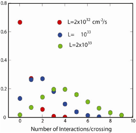
The bunch crossing rate at the LHCb interaction point (P8) is 40.08 MHz, while 2622 out of the theoretically possible 3564 crossings have protons in both bunches. Thus the maximum crossing rate with at least one pp interaction is 30 MHz. Figure 1 shows the change in the number of interactions per crossing as a function of the luminosity. At the present nominal luminosity, about 70% of the crossings are empty, while the others mostly contain a single interaction. At a luminosity of 1033cm-2s, there is a dramatic decrease in the number of empty crossings, but the average number of interactions per crossing is close to 1. However, already a luminosity of 2cm-2s augments the average number of interactions per crossing significantly. Thus the ability to disentangle topologies associated with multiple events becomes increasingly important to exploit the higher luminosity.
A very distinctive feature that can be used in designing hadron triggers that are highly efficient for heavy flavored meson decays produced in the LHCb event environment while retaining a high degree of rejection of the more common minimum bias events is the relatively long decay path of charm and beauty mesons. Detached vertex criteria are widely used in experiment operating at hadron machines, but typically they are introduced in the higher trigger levels. A strategy to incorporate these selection criteria in the lowest trigger level appears to be a promising avenue to implement the more robust and general hadron trigger that is a key component of the LHCb upgrade. This goal requires a strong connection between the SUPER-LHCb trigger and vertex detector design efforts. The limited granularity of strip detectors is such that an increased occupancy induces a higher fraction of the so-called “ghost tracks,” where a majority of the hits used are not coming from a single well defined physics track. Ghost tracks are very detrimental to any efficient detached vertex algorithm. They confuse the vertex topology and make the vertex reconstruction processors unnecessarily complex and time consuming.
3 The Present LHCb Vertex Detector System
The present VErtex LOcator (VELO) silicon detector system consists of 21 stations of silicon strip detectors positioned along the beam and perpendicular to the beam axis, as shown in Figure 2. Each station comprises two double sided modules that cover 1/2 of the acceptance. They are mounted on retractable stages, in order to protect the modules from excessive radiation damage during injection.
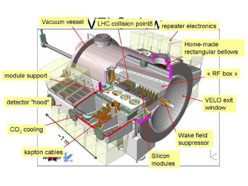
Two semi-circular sensors are glued back to back on a hybrid made of a carbon fiber/TPG (thermal pyrolytic graphite) with kapton flex circuits laminated on both sides to form a double sided module. The sensor active area span between 8 and 40 mm. Both of them comprise 2048 strips sensitive either to the radial (R) or azimuthal () coordinate in a cylindrical coordinate system where Z is along the beam axis. More details can be found in Ref. [2]. The hybrids host 16 front end ASICs (BEETLE) [3] that include 128 low noise fast analog processors. The analog outputs are stored in a 4 s deep analog pipeline and are read out upon the arrival of an L0 trigger signal through 4 LVDS lines, each 32 channel deep.
In addition, there are 4 R sensitive modules that are identified as “VETO stations,” which have the purpose of rejecting events with more than 1 interaction. The VETO stations will not be replaced in the planned upgrade, as we plan to process events with multiple interactions efficiently.
The LHCb detector configuration, which is oriented in the forward direction, implies a highly non-uniform irradiation of the silicon sensors in the vertex telescope. The innermost radius, being so close to the beam, will be exposed to 3.4 n per year at the nominal luminosity [4]. Thus the technology chosen for the VELO sensor is the -on- [5], adopted by the other LHC experiments for their inner tracking layers, where strips are implanted on -type substrate. Interstrip isolation is achieved with a blanket p-spray technique [6]. Even with this radiation hard implementation, it is expected that after few years of operation the VELO detector system will need to be replaced. Replacement module production is already underway. The sensor geometry is essentially unchanged, but the sensors are fabricated on -type substrates. Thus the detectors are easier to fabricate, as they require only single side processing and bear the promise of even greater radiation resistance [7].
4 SUPER-LHCb Vertex Detector Requirements
The LHCb vertex detector must have fast and robust pattern recognition capabilities, as it is going to be the heart of the separation between signal and background events on the basis of the vertex topology. Further improvements on the proper time resolution have a significant impact on the detector performance.
One alternative is a reduction of the amount of material in front of the fist sensing layer in the system. This implies a redesign of the RF shield, which is also the dominant contributor to the average radiation length of this detector system. A drastic solution would be a replacement of the RF shield with wires to screen the beam image currents. This approach may even enable to locate the innermost edge of the modules closer to the beam axis, with additional gains in proper time resolution.
Radiation resistance at unprecedented level is a key requirement to maintain stable operation during the accumulation a 100 fb-1 data set. The innermost region of the detector is expected to receive an integrated fluence of about 1016 1 MeV neq/cm2, comparable with the radiation exposure expected for the innermost tracking layers of the central SLHC detectors.
In order to exploit the higher interaction rate effectively, the front end device must be capable of delivering its information to back end receiving data boards in real time, namely the hit information should be time stamped and sent to the receiving end synchronously with the beam crossing frequency of 40 MHz. This requires fast front end electronics, a mechanism to push the data from the sensing element hit to the digital periphery without excessive delays, and large data rates from the detector to the remote electronics. This implies impressive data throughput capabilities.
Finally, an overall material minimization for any chosen solution is necessary to reduce the adverse effects of Multiple Coulomb scattering (MCS). This implies a careful design of the support and cooling systems, and an optimization of the number of modules and their geometry.
5 The VELOPIX Concept
The approach that has the best chance of satisfying the requirements described above relies on hybrid pixel sensors bump bonded to a custom made front end electronics which satisfies the requirements described above. This solution allows the a fast determination of space points that can be aggregated into tracks with relatively simple pattern recognition algorithms. In addition, the use of the pixel geometry would remove the constraint that the system is perfectly mechanically centered around the beam axis, to allow the R-z trigger scheme to operate.
As a consequence, vertex topology algorithms highly efficient for interesting hadronic events can be implemented in the first step of the selection process. This approach enhances the sensitivity to hadronic channels by at least a factor of 2, and is a selection algorithm that can be successfully exploited at higher luminosities. Significant advances towards a first level detached vertex trigger were achieved by the BTeV experiment [8]. The low occupancy, and ease in pattern recognition featured by vertex detector modules implemented with hybrid pixel technology are key elements in this approach.
Hybrid pixel devices are our preferred solution because they represent a mature and robust technology which allows to complete this project in the relatively stringent time scale envisaged ( 2015). This is a mature technology, having been perfected in the extensive BTeV R&D and in the development and production of the ATLAS and CMS vertex detectors. The hybrid approach allows for independent development and testing of the front end sensors and of the readout electronics.
There are several advantages associated with the reduced pixel area: the low input capacitance seen by the preamplifier in the front end electronics produces a corresponding low intrinsic noise (of the order of 100 e-), and a negligible common mode noise. This results in a higher signal to noise ratio than strip devices with the same detector thickness over a much longer radiation exposure. The extremely low noise occupancy is an advantage for pattern recognition, as well as the fine two dimensional detector segmentation.
5.1 VELOPIX Sensor
In general, sensors with small pixel dimension of approximately 50 m are a well developed technology. Two possible improvements to the standard sensor technology developed for the ATLAS and CMS pixel devices are currently considered. One of them is the implementation pixel devices with the -on- approach may present significant advantages in production yields and radiation resistance.
The closeness of the VELO silicon planes to the LHCb beam makes the issue of radiation hardness a primary concern. Several different approaches toward higher radiation sensitive devices are being tried in the framework of RD50 [9]. Prototype of strip and pixel sensors implemented with a variety of substrates (p-type, n-type both in float zone and magnetic Czochralski silicon substrates) have been manufactured, and exposed to different level of irradiation both from proton and neutron beams. Using the benchmark criteria of adequate collection properties at the highest levels of radiation fluence expected, silicon detectors developed on p-type substrates appear a promising option to achieve these results [10].
Recent multi-project wafer produced by collaborating institutions within the RD50 collaboration [9] have included pixel devices with a variety of geometries. In particular, pixel sensors compatible with the BTeV front end electronics have been designed with a joint effort between Fermilab and Syracuse University [11]. They have been characterized in the laboratory before irradiation, with excellent performance. The change in behavior upon irradiation is currently under investigation.
A solution that alleviates the need for very high (500-1000 V) reverse bias applied to the silicon devices to achieve adequate charge collection would provide significantly lower demands on the high voltage distribution system and on the cooling system. These “3D detectors,” constructed with Micro-Electro-Mechanical-Systems (MEMS) processing, are an innovative approach to segmented solid state detectors, where narrow holes and trenches are etched through silicon wafer and the back filled with conductive polysilicon (n and p doped). The depletion region is achieved with lateral bias, from electrodes as close as 50 m, thus requiring very modest high voltage. An additional advantage of this solution is the absence of guard ring, and the associated dead area. Almost edgeless devices can thus be implemented. This technology has been proposed by Parker and Kenney [12] in 1994, and it has undergone several years of intense development. Recent test beam data [13] have demonstrated that the technology proposed by Parker and Kenney can deliver the expected performance. The challenge is to develop a process for 3D detectors by an industrial Si device manufacturer. Several efforts are under way [13], [14], [15].
Finally, the impressive progress made by the RD42 collaboration in the development of carbon vapor deposition diamond detectors [16] suggests that this technology may be a viable solution for the innermost region of the detector plane, withstanding the highest levels of irradiation. Poly-crystalline and single crystal chemical vapor deposition (CVD) diamond can withstand fluences of the order of 10 neq/cm-2, with very competitive signal to noise performance and edgeless geometry [16]. Their low capacitance make them naturally a very low noise system, with added noise immunity. In addition, the leakage current remains remarkably low at all the levels of irradiation, thus making the cooling system much simpler [17].
5.2 VELOPIX Electronics
The goal to implement zero-suppressed analog readout with correct beam crossing assignment demands an active program in ASIC development, to produce a radically different front end device than the present BEETLE chip. The specifications on its architecture and data flow are closely connected with the overall data acquisition and trigger strategy. In particular, the studies of a detached vertex trigger influence the overall data flow architecture and may influence some aspects of the front end ASIC design.
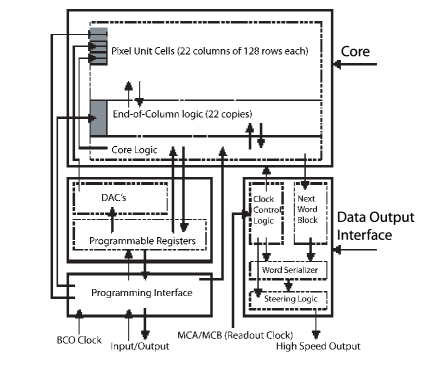
A promising prototype is the FPIX2 chip [19], developed for the BTeV pixel project. This device consists of an array of 22 columns of 128 cells of 50 by 400 m2. Figure 3 shows a schematic diagram of the FPIX2 pixel unit cell. It features a RC-CR preamplifier and shaper, eight comparators which provide zero suppression and form a 3-bit flash ADC and digital logic. The digital circuitry encodes the ADC information, and stores the hit information until an “output data” command is received from the end-of-column logic. Then data are transmitted to the data-output interface. The built in analog to digital conversion enhances the robustness of the system, as the information is transmitted in digital form, and the analog readout provides significant improvement in the spatial resolution [18]. In particular, a resolution between 6 and 9 m, dependent upon the track angle, was achieved with a pitch of 50 m. The lowest threshold is used for zero suppression, thus dramatically reducing the amount of information to be transmitted to the back end electronics. Changes to adapt this approach to the faster interaction rate and higher occupancy at LHCb are object of a planned R&D activity. The device is presently implemented in radiation tolerant mixed mode TSMC CMOS process. A readout bandwidth of more than 840 MBps has been demonstrated. It has been irradiated up to 87 MRad, without any degradation of the analog performance, and with only minor changes on the bias setting [19].
The group is also studying an adaptation of the TIMEPIX ASIC, developed by the MEDIPIX collaboration, which could allow the implementation of hybrid pixel systems with a square pixel geometry of roughly m2. This ASIC [20] contains a 256 256 matrix of square pixels. Each pixel processors includes a low noise analog front end, with digital readout based on the time over threshold technique. In the present implementation the pixel data are readout serially through an on-chip LVDS driver. A clock frequency of 100 MHz shifts out the information in less than 10 ms. A readout architecture consistent with the VELOPIX requirement needs to be implemented. This device is an evolution of the MEDIPIX2 ASIC, and is implemented in 0.25 m radiation tolerant CMOS technology. The new TIMEPIX for VELO is planned as an evolution of the MEDIPIX3 device [21], and is being designed in m CMOS technology.
5.3 Hybridization Issues
The detector electronics hybridization encompasses two main aspects, detector electronics connections, and interconnection between the readout ASIC and the periphery. A large body of experience on fine pitch bump bonding (down to a minimum pitch of 20 m [22]) has been accumulated in the course of the R&D and production of the large pixel devices developed for LHC. Bump bond yields 99.9 % on known good devices have been achieved. The most outstanding issue worth exploring with this approach is the minimum thickness that can be implemented both in the sensor and in the readout electronics. As irradiated devices have a collection length of the order of 100-150 m, this thickness is desirable for the sensor elements, while thinning of the readout electronics is limited by operation considerations [23] or mechanical stability issues.
The other connection required, between the hybrid detector ladders and periphery is typically implemented with flex-hybrid circuits, consisting of stacks of metallization layers separated by think polymid layers. Alternative options are offered by the MCM-D technique [22], where thin film technologies are used to deposit dielectric and conductor layers onto the bump side of the sensor layer. One of the advantages of this technique is the elimination of wire bonds, that make the handling of the detector element more challenging. An alternative path is offered by the “3D integration,” which the microelectronic industry consider key to meet the increasing power dissipation, speed, and signal integrity challenges posed by the newest CMOS technologies. For example, the Fermilab pixel group [23] has identified two different commercial processes implementing 3D integration that can be applicable to hybrid pixel devices. Hybrid modules, including pixel sensors bump bonded to FPIX2 electronics and thinned down to 100 m, have been characterized [24] with electronic test pulses, laser charge injection and radioactive sources. This work shows interesting results, in particular low input capacitance and good interconnection quality. Some of these technologies may allow to implement thinner hybrid modules with better signal integrity.
5.4 Mechanics and Cooling
There main issue that is being addressed in the mechanical design of the upgraded detector is the RF shield. On one hand it may need to be adapted to a different detector geometry, on the other hand thinning opportunities are very important as it is crossed prior to any position measurement and thus it has a strong influence on the spatial resolution achievable. A variety of options are being considered, from different material choices to shapes optimal for the new overall detector geometry.
Finally, cooling plays a critical role in the design of the upgraded detector. In particular, if the innermost portion of the detector is implemented with Si devices, a careful assessment of whether the present cooling can ensure a temperature that may ensures stable operation without thermal runaway is very important. Studies with different detector models, considering both the present evaporative CO2 cooling [25], and alternative options like the BTeV solution, where pixel modules were mounted on thermal pyrolytic graphite (TPG), which has excellent thermal conductivity, coupled with a liquid nitrogen cooled heat sink [26].
6 Conclusions
The LHCb experiment is at the eve of a very exciting physics program that will explore several facets of flavor physics with unprecedented precision. The VELO detector is a key component to achieve its physics goals. Radiation resistance and optimal performance in a hadron trigger in a high occupancy environment are the performance criteria guiding our R&D strategy towards the VELOPIX system. An essential component of this strategy is the implementation of a front end ASIC that features low noise readout, zero suppression, and data transmission in real time to the remote back end electronics that receives the local event fragments and assembles them in the event record.
7 Acknowledgements
This paper benefits tremendously from the work by many colleagues in the VELO Upgrade Group, and from the extensive discussions with T. Bowcock, P. Collins, C. Parkes, and S. Stone. This work was supported by the US National Science Foundation.
References
- [1] [LHCb Collaboration], “Expression of interest for an LHCb upgrade,”
- [2] [LHCb Collaboration], “LHCb VELO TDR: Vertex locator. Technical design report,”
- [3] M. Agari et al., Nucl. Instrum. Meth. A 518, 468 (2004).
- [4] G. Corti and L. Shekhtman, LHCB-2003-83 (2003).
- [5] G. Casse, Nucl. Instr. and Meth. A 566 (2006) 26.
- [6] T. Rohe, Nucl. Instr. and Meth. A460, 55 (2001).
- [7] G. Casse, Nucl. Instrum. Meth. A 579, 623 (2007).
- [8] E. E. Gottschalk [BTeV Collaboration], Nucl. Phys. Proc. Suppl. 156, 252 (2006).
- [9] The RD50 Collaboration, http://www.cern.ch/rd50.
- [10] G. Casse, P.P. Allport, and A. Watson, Nucl. Instr. and Meth. A568 (2006) 46.
- [11] M. Artuso, Nucl. Instrum. Meth. A 582, 835 (2007) [arXiv:physics/0701270].
- [12] C. Kenney, S. Parker, J. Segal and C. Storment,
- [13] A. Kok et al., Nucl. Instrum. Meth. A 560, 127 (2006).
- [14] D. Pennicard et al., IEEE Trans. Nucl. Sci., V. 54, 4, 1435 (2007).
- [15] A. Boscardin et al., Nucl. Instrum. Meth. A 570, 317 (2007).
- [16] M. Mathes, M. Cristinziani, H. Kagan, S. Smith, W. Trischuk, J. Velthuis and N. Wermes, JINST 3, P12002 (2008) [arXiv:0810.2080 [physics.ins-det]].
- [17] http://cdsweb.cern.ch/record/1009654/files/lhcc-2007-002.pdf
- [18] J. A. Appel et al., Nucl. Instrum. Meth. A 485, 411 (2002) [arXiv:hep-ex/0108014].
- [19] D. Christian et al., Nucl. Instr. Meth. A 549, 165 (2007).
- [20] X. Llopart et al., Nucl. Instr. Meth. A 581, 485 (2007); erratum Nucl. Instr. Meth. A 585 106 (2008).
- [21] R. Ballabriga et al., IEEE Trans. Nucl. Sci. 54 1824 (2007).
- [22] S. Konig, PoS VERTEX2007, 010 (2007).
- [23] R. Lipton and f. t. F. Group [Linear Collider Collaboration], arXiv:0901.4741 [physics.ins-det].
- [24] Z. Ye and f. t. F. Group, arXiv:0902.2801 [physics.ins-det].
- [25] M. van Beuzekom, A. Van Lysebetten and B. Verlaat, PoS VERTEX2007, 009 (2007).
- [26] A. Kulyavtsev et al. [BTeV Collaboration],