Shot noise of a ferromagnetic nanowire with a domain wall
Abstract
We study shot noise of the spin-polarized current in a diffusive ferromagnetic nanowire which contains a ballistic domain wall. We find that the existence of a short domain wall influences strongly the shot noise for sufficiently high spin-polarization of the wire. Compared to the situation of absence of the domain wall, the shot noise can be reduced or enhanced depending on the length of the domain wall and its relative conductance.
pacs:
72.10.-d, 75.47.Jn, 75.75.+a, 74.40.+kI Introduction
Electronic transport through ferromagnetic domain walls (DWs), the regions with rotating magnetization vectors which connect two homogeneous domains with miss-oriented magnetizations, has been recently a subject of extensive investigations, both theoreticallyTatara08 and experimentallyKent01 ; Marrows05 . This growing interest is stimulated by the fundamental new physics raising from the dynamics of spin of electron in DWMaekawa02 , as well as by the potential applications in nanoelectronics and spintronics devicesParkin02 . Among the others, recent experiments on magnetic nanostructures and nanowires have revealed that the presence of a DW may result in a magnetoresistance as large as several hundreds or even thousands of percentsGarcia99 ; Chopra02 ; Ruster03 .
In the bulk metallic ferromagnets like Fe, Co and Ni the so called Bloch walls are the favor magnetic configurations where the rotating magnetization vector is in the plane of DW. Such a DW is rather thick with a length of about several hundreds . However, in ferromagnetic nanowires the so called “Néel wall”s are more favored due to the transverse confinementEbels00 . In a “Néel wall” the magnetization vector rotates in the plane perpendicular to the plane of DW and the thickness of the DW can be of order of . In ferromagnetic nanostructures, like a narrow constriction between to wider domains, even sharper DWs with lengths of the atomic scale can appear Bruno99 ; Pietzsch00 ; aui03 . In the two latter cases the length of DW is usually smaller than the electron mean free path of scattering from the static disorders, and thus the electron transport is ballistic. Several theoretical works have been devoted to studying contribution of the ballistic DWs on the resistance of the nanowires and magnetic nanostructuresHoof99 ; Brataas99 ; Zhuravlev03 ; Dugaev05 . In a very thick DW the spin of the electron propagating across the wall follows the magnetization direction quasi-adiabatically. Then scattering of the electron from DW is very small and contribution of the DW in the resistance is negligibleCabrera74 ; Levy97 ; Tatara97 ; Gorkom99 . While for a narrow DW the dynamic of spin of electron through the wall is not adiabatic and the presence of the DW causes to considerable scattering of electron. Calculations in the ballistic regime show an increase of the resistance due to the DWImamura00 ; Dugaev03 ; Gopar04 ; Fallon04 .
In spite of several theoretical and experimental studies of the contribution of a DW on the average current, to our best knowledge, there have been no works devoted to the fluctuation of spin-polarized current in DWs. Low temperature temporal fluctuation of the electrical current through a mesoscopic conducting structure, the so called shot noise, provides valuable information about the charge transport process which are not extractable from the mean conductanceBlanter00 ; Belzig04 ; Zareyan05 ; Zareyan005 ; Hatami06 . The aim of the present work is to study the effect of spin-dependent scattering of electrons in a ferromagnetic DW on the shot noise.
We consider a ferromagnetic nanowire consisting of a ballistic DW connected to two diffusive domains with the magnetization vectors aligned antiparallel to each other. Employing the two-band Stoner Hamiltonian and within the scattering formalism, we calculate the spin-dependent transmission coefficients of DW. The resulting shot noise shows strong dependence on the size of the DW as well as the degree of the spin-polarization of the nanowire. For a thick DW where the spin-dynamic is dominated by the quasi-adiabatic following of the local magnetization vector, the shot noise has its normal value (shot noise of the wire without DW) determined solely by the conductances of the diffusive domains and the DW itself. However at lower thickness of DW, the shot noise deviates significantly from the normal value depending on the spin-polarization and the ratio of the conductance of the DW to the domains. The interplay between diffusive transport at domains and the noncollinear magnetization of the DW causes to reduction of the shot noise below the normal value with varying the DW thickness.
In the next section, we introduce a circuit which models the diffusive ferromagnetic nanowire with a ballistic Néel DW. We calculate the spin-polarized scattering coefficients of DW, which are essential for the calculations of the contribution of DW in the shot noise. Section III is devoted to developing formulas for the average current and the shot noise of the nanowire. We analyze the obtained results in section IV, for a full range of the DW thickness, the spin-polarization and the relative conductance of DW. Finally, in section V we give a conclusion.
II Modeling and the basic equations
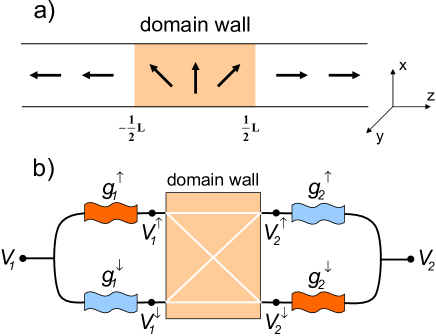
We consider a ferromagnetic nanowire consisting of two diffusive ferromagnetic domains with antiparallel magnetization vectors which are connected through a ballistic DW with length . Fig. 1. shows a sketch of the nanowire and the corresponding circuite consisting of the two diffusive domains and the ballistic DW. In the absence of extrinsic spin-flip scattering processes (for instance due to magnetic impurities), each diffusive domain is represented by two parallel spin-dependent conductances. In the circuit model the DW is represented as a coherent four-terminal scattering region which is connected through ideal ferromagnetic leads to conducting elements of the two domains (see Fig. 1b). We use the scattering approach and follow the Refs.[Levy97, ,Gorkom99, ,Gopar04, ] to calculate the scattering coefficients of the electron through the DW. Within the two-band Stoner model, where the -band electrons are responsible for the magnetization and the current is carried by the -band electrons, we may describe transport of the electrons through DW by an effective Hamiltonian of the form
| (1) |
where is the spin splitting of the electrons due to the exchange coupling with the electrons and is the vector of the Pauli matrices. First term of the Hamiltonian is the kinetic energy of electron and the second part represents the interaction of the spin of electron with the local magnetization oriented in the direction of the unit vector . In this work we consider a “Néel wall”, which is more common configuration in laterally confined ferromagnetic nanowires. We assume that varies along the direction (wire axis). In the left and right domains the magnetization vectors are aligned along the and axis, respectively. The assumption allows us to separate the transverse and longitudinal parts of the Hamiltonian (1). In the transverse direction the motion of the electron is quantized with an energy denoted by . From Eq. (1) the effective Schrodinger equation for the longitudinal motion of electron is obtained as
| (2) |
where is the longitudinal energy. To be specific we consider a trigonometric magnetization profile in the DW, which is defined by Gopar04
| (3) |
The advantage of this choice is that, it admits an exact solution for the wave functions inside the DW.
In order to obtain the spin-dependent transmission and reflection coefficients we have to solve the Schrodinger equation (2) in different regions and then match the solutions of different regions at the boundaries (). In the domains and the eigenfunctions have the form , where denote up and down spin directions and are the spin states when spin quantization axis is chosen to be the axis. The longitudinal wave vector for spin- electrons is given by . To find the eigenfunctions in the DW we do a transformation in spin space from the fixed reference frame to the rotated frame, which is in the direction of the local magnetization vector . In our representation it is given by a rotation about the axis , where is the angle of the magnetization vector respect to the axis at the point . The Hamiltonian in the rotating frame , where is the longitudinal part of the Hamiltonian at fixed frame, takes the form
| (4) |
which does not depend on explicitly. Here . The eigenfunctions of this Hamiltonian have the forms
| (10) |
where
| (11) |
and the longitudinal wave vectors are
| (12) |
The wave functions in the fixed reference frame (along z axis) are obtained from the relations . Now, if we consider a spin up electron incident to the DW from the left domain, the wave functions in three regions have the following forms
| (13) |
for ,
| (18) | |||||
| (23) |
for and
| (24) |
for . Here () and () are the spin-conserved and spin-flip transmission (reflection) coefficients, respectively. Imposing the condition of the continuity of the wave functions and their first derivatives at the boundaries (), we obtain these scattering coefficients. The obtained expressions are too lengthly to be given here. We only mention some properties of the reflection and transmission probabilities. Both spin-conserved and spin-flip reflection probabilities are small except for a narrow DW of the length , where is the spin-polarization dependent length scale. The spin-conserved transmission probability , is close to unity for a narrow DW, and has a diminishing behavior with increasing toward a vanishing value for a thick DW. In contrast the spin-flip transmission probability , has an appreciable value for a sizable DW of , where the spin of electron has enough time to follow adiabatically the local magnetization direction. In the limit of the electron transport is mainly realized through two independent channels connecting the majority and minority spin electrons in two domains.
III Average current and Shot noise
To express the average current and shot noise of the nanowire in terms of the scattering coefficients derived in the previous section, we use the the circuit model of nanowire shown in Fig. 1b. In the circuite the diffusive domains are modeled by two parallel conductances for up and down spin electrons, denoted by , where labels the left and right domains, respectively. These conductances have connected to the left and right reservoirs with fixed voltages and . The DW has been shown as a four terminal device connected via the nodes (,) to the same domains through the ideal ferromagnetic leads. For simplicity we consider a symmetric structure for that . Noting the fact that the difference of the Fermi level density of states for the majority and minority spin electrons in the domains is proportional to the ratio , the spin-dependent conductances are approximated by
| (25) |
where is the total conductance of each diffusive ferromagnetic domain. The conductance of the ballistic leads is given by , where the total number of open channels in the leads is the sum of the number of open channels for two spin states electrons . The value of is normally large in ferromagnetic domain structures.
We derive the average current and the shot noise power from the spin-dependent Landauer-Buttiker formula Buttiker92 and the scattering coefficients obtained in the previous section. The current operator for spin- electrons flowing through terminal is defined as
| (26) | |||||
where the operator creates (annihilates) outgoing electron from terminal in the nth channel with energy . Similarly, , () denotes creation (annihilates) operator for a spin- incoming electron in the terminal . The corresponding average current reads
| (27) |
where , stand for domains and , for spin directions; are spin- voltages at the connecting nodes between the domain and the DW, and are elements of the conductance matrix defined by
| (28) |
where are elements of the scattering matrix of the DW at the Fermi energy. Considering that the number of channels is very large and using the fact that the density of states for a 2D system is constant we can change the to integral over in calculating the traces. Then we can write
| (29) |
The corresponding expression for the zero-frequency correlation of current fluctuations is expressed as
| (30) |
On the other hand the average current for spin- electrons through the domain can be obtained via the relation
| (31) |
Applying the conservation rule for spin- current flowing into the nodes (,) and using Eqs. (27) and (31) we find
| (32) |
The solution of this matrix equation give us in terms of the voltage difference (), the conductances and , from which and using Eqs. (27, III) we can calculate the spin-resolved average currents and the contribution of DW to the correlations of current fluctuations in different nodes.
To calculate the noise power of the total charge current in reservoir , we should include the effect of the voltage fluctuations in the nodes as well as the fluctuations due to the scattering inside the domains. Using equation (31) and denoting the intrinsic fluctuations of the current due to the scattering inside the domain by , we can write the total fluctuations of the spin- current coming from domain to the (,) node as
| (33) |
where is the voltage fluctuation in the node (,). We notice that the voltages of reservoirs are constant. At the same time from Eq. (27) we obtain the total fluctuation of the current flowing through the node (,) in terms of the current fluctuation due to scattering from DW:
| (34) |
where is the intrinsic current fluctuation of DW. Applying the conservation rule for the temporal fluctuations of the currents , we obtain
| (35) |
By solving the above matrix equation we find in terms of the and . The shot noise of the total current in reservoir is given by
| (36) |
where , and is expressed in terms of the correlations of the current fluctuations and . The correlations of the currents fluctuations are given by Eq. (III), and for the diffusive domains we have the following result for the correlations of the currents
| (37) |
Using Eqs. (31), (36), (37) and (III) we can calculate the average current and the shot noise of the nanowire in terms of the system parameters. In the next section we discuss the results for average current and Fano factor defined by .
IV Results and Discussions
The average current and Fano factor of the nanowire can be expressed in terms of the three dimensionless parameters , and which respectively characterize the thickness of the DW, the degree of spin-polarization of the nanowire and the relative conductance of the ballistic DW and the two domains.
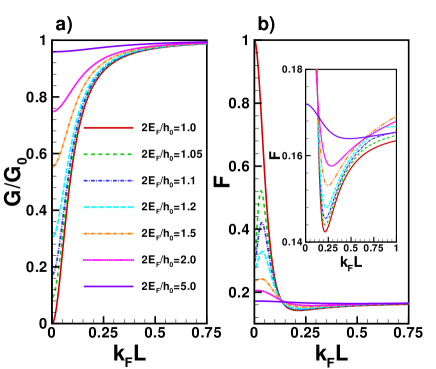
Let us start with analyzing the effect of DW in the conductance of the nanowire. In Fig. 2a, we have plotted the conductance of the nanowire normalized to its conductance in the absence of DW, , versus for and different values of . Conductance of the nanowire rises with increasing the thickness of the DW, which means that the presence of the DW always increases resistance of the nanowire. Considerable change in the conductance occurs for a short DW. The corresponding variation of the Fano factor is shown in Fig. 2b. For the half metal nanowire () the Fano factor approaches its maximum Poissonian value () at small lengths but decreases rapidly by increasing . In a fully polarized nanowire at small lengths the DW acts as a tunnel barrier and causes to Poissonian shot noise. A similar effect is seen in the FNF spin valve structuresZareyan05 . The Fano factor passes through a smooth minimum before taking its normal value in the limit of . For smaller spin-polarizations (greater values of the ) the Fano factor shows a maximum smaller than one which occurs at a finite . The smooth minima at a finite length of DW occurs for smaller spin-polarizations as for the case of , as is shown in the inset of Fig. 2b. This observation that the Fano factor decreases below its normal value for specific lengths of DW can be attributed to the noncollinear change of the magnetization at DW. Increasing causes a decrease in the spin conserving transmission coefficient and an increase in the spin-flip transmission coefficient. This tends to decrease the Fano factor. At the same time by increasing the length of the DW, its conductance increases and consequently the contribution of the domains in the Fano factor increases. Competition of these two effects leads to generation of the minimum in the Fano factor, such that goes below the normal value. In this regime while the transport of electron through DW is closely ballistic giving rise to a negligibly small shot noise, its conductance has a sizable value to have a significant contribution to the Fano factor of the whole structure. A similar behavior has been seen in the noncollinear FNF systems with diffusive junctionsTserkovnyak01 ; Abdollahi06 , where the Fano factor reduces below its collinear value at specific values of the relative angle of the magnetization vectors. In the limit of large the Fano factor tends to its normal value (single domain ferromagnetic nanowire) given by
| (38) |
where denotes majority and minority spin sub-bands, and are Fano factors and resistances of the domains, and are those of very thick DW. This expression coincides with the results which is obtained by extending the formula derived by Beenakker and Buttiker for Fano factor of a wire consisting of a series of phase coherent segments in the inelastic regimeBeenakker92 . At this limit electrons pass adiabatically trough the DW and mixing between majority and minority spin sub-bands is negligible. Thus system behaves like a single domain and DW has no considerable effect on the conduction.
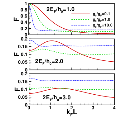
Let us now consider the effect of varying the relative conductances of domains on the Fano factor. This is shown in Fig. 3 for different . The main feature is that by decreasing the length scale over which has appreciable variation increases. There are two contributions in the total shot noise of the nanowire. One is the domains contribution which is independent of the DW length and the other one is due to the DW and depends on the length of the DW. The relative importance of them is determined by voltage drops at these elements. For large domains act as resistive elements of the nanowire and cause to lowering the voltage drop at DW and thus reducing the importance of the DW contribution. As it is seen in the figure (3) at this limit the Fano factor shows small variations whit length. On the opposite limit when is small the DW has dominant contribution at the shot noise and the the Fano factor shows considerable variations whit length of DW.
V Conclusion
In conclusion, we have investigated the effect of a ballistic domain wall on the spin-polarized shot noise of a ferromagnetic nanowire. We have considered the inelastic regime where the diffusive domains and the ballistic DW can be treated as the separated coherent segments. Using the two-band Stoner model for a Néel type trigonometric profile of the magnetization vector, we have obtained that Fano factor changes significantly with respect to its value in the absence of DW for a high spin-polarization of the wire and when DW is short enough. A remarkable result is that the presence of DW can cause both reduction or enhancement of the shot noise, depending on its length, the spin-polarization and the relative conductances of the domains and DW. Here we considered an especial type of the profile for the DW. The realistic profile of a DW can be different. Since different profiles for the DW do not change the scattering coefficients qualitativelyGopar04 , we expect that the simplified profile we considered here will capture the essential physics and the effect of considering other profiles to our results for shot noise will be minor and quantitative.
With the new developed techniques for measurement of the shot noise in various systems especially the magnetic tunnel junctionsGuerrero08 and recent progresses in fabricating and controlling different types of DWsMarrows05 , the shot noise measurement in DW seems to be feasible. Such future measurements can verify our results experimentally.
References
- (1) G. Tatara, H. Kohno, J. Shibata, Phys. Rep. 468, 213-301 (2008).
- (2) A. D. Kent, J. Yu, U. R diger, and S. S. P. Parkin, J. Phys.: Cond. Matt. 13, R461 (2001).
- (3) C. H. Marrows, Advances in Physics, 54, 585(2005).
- (4) Spin Dependent Transport in Magnetic Nanostructures, edited by S. Maekawa and T. Shinjo (Taylor and Francis, London and New York, 2002).
- (5) S. S. P. Parkin, Applications of Magnetic Nanostructurs, Vol. 3 of Advances in Condensed Matter Science (Taylor and Francis, New York, 2002).
- (6) N. Garc ia, M. Munoz, and Y. W. Zhao, Phys. Rev. Lett. 82, 2923 (1999); G. Tatara, Y. W. Zhao, M. Munoz, and N. Garc ia, Phys. Rev. Lett. 83, 2030 (1999).
- (7) H. D. Chopra and S. Z. Hua, Phys. Rev. B 66, 020403(R) (2002); S. Z. Hua and H. D. Chopra, Phys. Rev. B 67, 060401(R) (2003).
- (8) C. R uster, T. Borzenko, C. Gould, G. Schmidt, L. W. Molenkamp, X. Liu, T. J. Wojtowicz, J. K. Furdyna, Z. G. Yu, and M. E. Flatt e, Phys. Rev. Lett. 91, 216602 (2003).
- (9) U. Ebels, A. Radulescu, Y. Henry, L. Piraux, and K.Ounadjela, Phys. Rev. Lett. 84, 983 (2000).
- (10) P. Bruno, Phys. Rev. Lett. 83, 2425 (1999).
- (11) O. Pietzsch, A. Kubetzka, M. Bode, and R.Wiesendanger, Phys. Rev. Lett. 84, 5212 (2000).
- (12) M. Kl aui et al., Phys. Rev. Lett. 90, 097202 (2003).
- (13) J. B. A. N. van Hoof, K. M. Schep, A. Brataas, G. E. W. Bauer, and P. J. Kelly, Phys. Rev. B 59, 138 (1999).
- (14) A. Brataas, G. Tatara, G. E. W. Bauer, Phys. Rev. B 60, 3406 (1999) .
- (15) M. Ye. Zhuravlev, E. Y. Tsymbal, S. S. Jaswal, A. V. Vedyayev, and B. Dieni, Appl. Phys. Lett. 83, 3534 (2003).
- (16) V. K. Dugaev, J. Barna s, J. Berakdar, V. I. Ivanov, W. Dobrowolski, and V. F. Mitin, Phys. Rev. B 71, 024430 (2005).
- (17) G. G. Cabrera and L. M. Falicov, Phys. Status Solidi B 61, 539 (1974); 62, 217 (1974).
- (18) P. M. Levy and S. Zhang, Phys. Rev. Lett. 79, 5110 (1997).
- (19) G. Tatara and H. Fukuyama, Phys. Rev. Lett. 78, 3773 (1997).
- (20) R. P. van Gorkom, A. Brataas, and G. E. W. Bauer, Phys. Rev. Lett. 83, 4401 (1999).
- (21) H. Imamura, N. Kobayashi, S. Takahashi, and S. Maekawa, Phys. Rev. Lett. 84, 1003 (2000).
- (22) V. K. Dugaev, J. Berakdar, and J. Barna s, Phys. Rev. B 68, 104434 (2003);
- (23) V. A. Gopar, Dietmar Weinmann, Rodolfo A. Jalabert, and Robert L. Stamps, Phys. Rev. B 69, 014426 (2004).
- (24) Peter E. Falloon, Rodolfo A. Jalabert, Dietmar Weinmann, and Robert L. Stamps, Phys. Rev. B 70, 174424 (2004).
- (25) Ya. M. Blanter and M. Büttiker, Phys. Rep. 336, 1 (2000).
- (26) W. Belzig and M. Zareyan, Phys. Rev. B 69, 140407(R) (2004).
- (27) M. Zareyan and W. Belzig, Phys. Rev. B 71, 184403 (2005).
- (28) M. Zareyan and W. Belzig, Eur. Phys. Lett. 70, 817 (2005).
- (29) M. Hatami and M. Zareyan, Phys. Rev. B 73, 172409 (2006)
- (30) M. Buttiker, Phys. Rev. B 46, 12485 (1992).
- (31) Y. Tserkovnyak and A. Brataas, Phys. Rev. B 64, 214402 (2001).
- (32) B. Abdollahipour and M. Zareyan, Phys. Rev. B 73, 214442 (2006).
- (33) C. W. J. Beenakker and M. Buttiker, Phys. Rev. B 46, 1889(R) (1992).
- (34) R. Guerrero, F. G. Aliev, Y. Tserkovnyak, T. S. Santos, and J. S. Moodera, Phys. Rev. Lett. 97, 266602 (2006).