An essential mechanism of heat dissipation in carbon nanotube electronics
Abstract
Excess heat generated in integrated circuits is one of the major problems of modern electronics. Surface phonon-polariton scattering is shown here to be the dominant mechanism for hot charge carrier energy dissipation in a nanotube device fabricated on a polar substrate, such as . Using microscopic quantum models the Joule losses were calculated for the various energy dissipation channels as a function of the electric field, doping, and temperature. The polariton mechanism must be taken into account to obtain an accurate estimate of the effective thermal coupling of the non-suspended nanotube to the substrate, which was found to be 0.1-0.2 W/m.K even in the absence of the bare phononic thermal coupling.
Introduction
Nowadays the vast majority of human activities are supported by advanced information technology which cannot become a transformative power without progress in semiconductor electronics. Exponentially increasing dissipated power density in integrated electronics circuits is one of the “grand challenges” of modern electronics heat-in-ic ; crchandbook . Excess heat generated by electric currents in the elements of circuits cannot be completely removed because of the high power density, which leads elevated device operation temperatures, performance reduction, and ultimately results in hardware failures.
Heat dissipation takes place via the transfer of thermal energy that is generated by hot charge carriers, to the cooling units eventually. The three classical mechanisms of heat transfer are convection, conduction, and radiation. The former is inapplicable in existing circuit architecture having no fluid or gas flowing inside. The latter has a total emissive power proportional to according to the Stefan -Boltzmann law, and is not very effective within the acceptable range of temperatures SBnearfield ; fnote1 . Thus the major mechanism responsible for the device cooling is the thermal conductance. High thermal conductance can be achieved in bulk solids, but even a small vacuum gap is a quite effective thermal insulator.
This is the case for transistor channels involving a nanostructure, for example a nanowire or a nanotubeavouris-dev ; lieber1 ; lieber2 , which is not chemically connected to the substrate, instead it is bound by relatively weaker van der Waals forces. This weak binding has a positive effect on the mobility of the charge carriers, but also has a negative effect on the thermal conductance. In existing nanotube transistors only the contacts have a good thermal exchange rate while the thermal conductance over the van der Waals separation gap is very low, of the order of 0.05–0.2 therm-cond-exp-theor1 ; therm-cond-exp-theor2 ; therm-cond-exp-theor3 ; therm-cond-exp-theor4 ; therm-cond-exp-theor5 . In addition, the total thermal conductance of the contacts is not too high, being proportional to the cross-sectional area of the nanotube.
In this work we propose that a fourth mechanism of heat dissipation from the hot charge carriers in the nanotube channel into a polar substrate should operate and argue that such a mechanism would dominate the thermal transfer especially at large device currents (high bias voltages). Understanding the importance of such a mechanism invokes concepts that are specific to carbon nanotube (NT) field-effect transistors (FET): low thermal conductance due to the van der Waals separation gap (and possible surfactant coating) and the small contact area, high Fermi velocity of the NT charge carriers and the existence of the special electromagnetic (EM) surface modes in the vicinity of the NT channel. Hot electrons, as we will discuss below, can excite surface polariton modes. This mechanism while important for nanoscale channels is ineffective in a macroscopic system because the EM field of the polariton decays exponentially with the distance from the surface plane polder . This leads to a power low scaling of the scattering rate with the distance from the surface plane p-subm . A surface polariton mode would quickly dissipate into bulk substrate modes, thus providing a heat transfer mechanism with an efficiency exceeding the standard thermal conductance or radiation mechanisms.
The existence of surface polariton modes was predicted in 1899 sommerfeld and were later observed at AM radio-wave frequencies. In condensed matter, a metal surface is known to support surface EM modes that is plasmon-polaritons; the focus of recent plasmonics studies plasmonics . The plasmon-polariton EM mode exists if the real part of the dielectric function of the substrate equals negative one mahan . Similarly, one can observe a surface polariton in a polar insulator where a strong optical phonon mode provides the required condition: . Then the frequency of the surface phonon-polariton (SPP) is close to the frequency of the optical phonon. For example, for a SiO2 surface the optical phonon modes that can support SPP are at 50, 62, 100 and 149 meV quartz1 ; lynch ; spitzer . Hot charge carriers in a NT FET with energy exceeding the polariton energy would effectively release energy into the SPP channel.
We stress that despite the fact that this mechanism is similar to a classical one for hot charge carrier energy relaxation whereby the energy dissipates into optical phonons of the NT kane ; javey ; park ; perebeinos , the SPP mechanism transfers the thermal energy directly into a bulk substrate, while the classical one only redistributes it between the NT electrons and the NT lattice, to be followed by thermal conduction into the leads and/or the substrate. The SPP mechanism also differs from the classical radiation since the charge carriers in the channel couple to the evanescent EM modes only. The greatly enhanced surface electric field of such modes has much larger overlap with the NT channel than it would be in the case of the free vacuum EM modesfnote1 .
Simulation approach
We have adopted the model described in detail in the previous works perebeinos ; p-subm ; perebeinos2 . In brief, a standard tight-binding Hamiltonian for the NT charge carriers, , is supplemented with Su-Schrieffer-Heeger terms for the electron-NT-lattice-phonon coupling (Eq.(1) of Ref.perebeinos ):
| (1) |
here the matrix element of the interaction is eV/Å. The coupling constant is , where eV is the bare tight-binding hopping integral being modulated by the phonon modes. and are annihilation operators for NT phonons ( is a phonon branch index) and charge carriers in conduction and valence bands, respectively, that are labeled with the one-dimensional axial momentum or . In addition to the NT lattice phonons we include the operator of the interaction with the SPP mode (cf. Eq.(2) in Ref.jetpl ):
| (2) |
where is the annihilation operator for the -th surface phonon mode (not to be confused with the NT lattice phonons), and an explicit form of was derived in Ref.jetpl :
| (3) |
here and are the components of the SPP momentum that are parallel and normal to the NT axis respectively (see Fig.1c), is the angular momentum transfer to the SPP mode (equals 0 in case of the NT intra-subband scattering which is the strongest scattering channel), is the NT radius, Å is the distance from the NT axis to the surface, is the Bessel function of imaginary argument abramovitz . is the elementary charge and characterizes the strength the electric field of the SPP mode mahan :
| (4) |
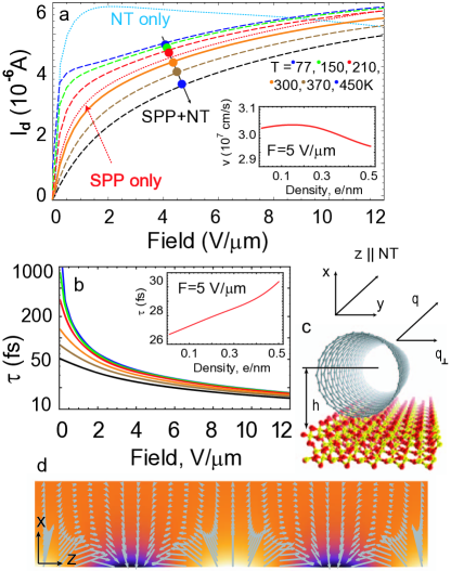
where is the normalization surface area, is the frequency of the longitudinal optical phonon of the polar substrate with the static permittivity and the low-frequency dielectric function . We should emphasize that while there are four surface modes present (the highest energy one being doubly degenerate), only two of them have strong coupling strength p-subm ; jetpl : . The characteristic distribution of the electric field of the SPP mode above the substrate surface is shown in Fig.1d. The field oscillates along the surface (along ) and decays exponentially in the space (along ). The transverse component of the SPP momentum, , is not conserved and has to be integrated for the final result.
To simulate the current-voltage curves we solved numerically the steady-state Boltzmann equation for the NT in a constant electric field (including as many subbands as needed for given temperature and drain field values). One can assume that in the bulk of the FET channel the drain voltage is related to the applied electric field via the effective channel length : . The scattering rates for the Boltzmann equation are as follows (see Refs.p-subm and jetpl for further details):
| (5) |
here is the frequency of the SPP mode mahan ; its phonon occupation number, is the energy of the final/initial state as obtained from the Hamiltonian . Non-equilibrium distribution function has been calculated numerically for every given value of the temperature, field and charge density and then it was used to compute the total electron current, , as well as to determine the partial phonon emission rates for the heat dissipated in the NT lattice and that dissipated directly into the substrate via the SPP mode , according to:
| (6) |
where are the total Joule losses. A similar equation holds for NT losses with the scattering rate obtained from Eq. (1). In the following we study dependencies of the SPP to the NT channel loss ratio, defined as , on the bias, density, and temperature.
SPP Scattering and NT-FET High Bias Regime
The role of the SPP modes with respect to charge carrier scattering (so-called Remote Interface Phonon scattering) for Si devices has been first studied by Hess and Vogl vogl , though this mechanism was not found to dominate the transport siRIP . As we show in this work, for nanotube devices the SPP scattering mechanism is very fast, as been indicated already in our earlier paper jetpl and cannot be neglected even for the low-field transport p-subm .
The SPP energy relaxation rate exceeds the intrinsic NT phonon relaxation rates (for both optical and acoustic modes) for the whole range of the charge densities and applied electric fields (gate and drain biases) studied here as shown by the results in Fig. 1b.
Recently SPP scattering was demonstrated to determine the mobility in graphene on a polar substrate and to limit the ultimate performance of graphene devices fuhrer-n-theory1 ; fuhrer-n-theory2 ; ken-n . Fig.1a shows typical current-electric field curves calculated with and without the SPP mechanism taken into account. Neglecting the SPP channel significantly overestimates the low-field current. Two important conclusions are drawn from these data: firstly, the negative differential resistance region of the current-voltage characteristic is totally removed when the SPP channel included, because the very effective SPP energy relaxation prevents the hot electron run-away as we further discuss in Ref. p-subm . Secondly, the SPP mechanism dominates over the NT phonon scattering for both low- and high-field regimes but the remnants of the non-SPP behavior can be seen at low applied field especially at low temperature.
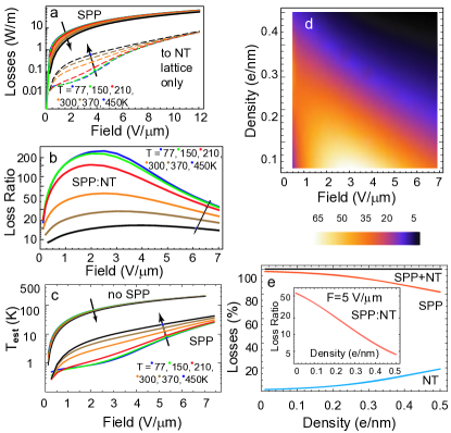
Results on the relative importance of the SPP and NT-phonon scattering channels for the energy relaxation of the hot charge carriers are shown in Fig.2. In Fig.2(a) we plot, in a logarithmic scale, the partial specific energy losses due to the SPP channel (full curves) and only the NT phonon channel (broken curves), calculated for [17,0] NT at the doping level at various temperatures. The SPP losses are up to two orders of magnitude larger than the NT phonon losses. Fig.2(b) presents the ratio of the SPP partial losses to the NT phonon partial losses calculated for the same NT. The high frequency NT optical phonons increase the NT partial losses at higher fields and higher (Fig.2b). Even in that limit their ratio is always greater than one.
We also studied the dependence of the loss ratio on the doping level (Fig.2e, inset) at the fixed applied electric field . The relative decrease of the SPP contribution at higher electron density (higher gate bias) is shown in Fig.2(e) as a percentage of the total losses and is due to the SPP and NT phonon losses having a different functional dependence on . The non-equilibrium distribution function (obtained as a numerical solution of the Boltzmann equation) varies with the doping level. The SPP losses, correlated with the non-equilibrium distribution function, scale similar to the total losses (proportional to the current) and are approximately a linear function of the doping level (total number of electrons). The NT phonon losses are superlinear in and grow faster, thus their ratio decreases with .
To understand the dependencies of the NT and SPP losses on field strength and temperature, we show the scattering rate of electrons via these two channels in different bands as a function of energy (see Supplemental Information Fig. 3). In the first two energy bands the SPP scattering dominates over the NT scattering, while in the higher energy bands the NT scattering becomes comparable to that of the SPP scattering. This is because in the SPP scattering the angular momentum is conserved , so that only intra-band scattering takes place, while NT optical phonons can lead to both intra and inter-band scattering and the phase space for such scattering grows with the band index. Therefore, as the electronic distribution becomes hotter either due to the field or temperature the relative role of the NT phonons increases and the loss ratio decreases. Fig. 4S (Supplemental Information) further supports that the electronic distribution function rather than the scattering rate (see Eq. (6)) is primarily responsible for the value of the loss ratio at the high bias regime. Therefore the NT and SPP losses scale in exactly the opposite way with temperature.
Near-Field Thermal Conductance and Self-Heating of NT-FET Channel
Next we discuss another aspect of SPP scattering, namely we address how the heat generation is controlled by the fast SPP energy relaxation rates.
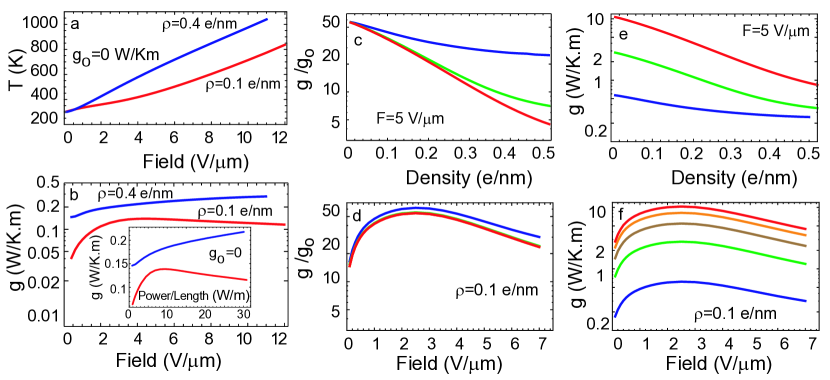
So far we set the NT temperature equal the substrate temperature. That is we assumed an ideal thermal coupling to the substrate which is a condition not confirmed experimentally. As a next level of approximation we use thermal coupling values (per NT length) from the literature therm-cond-exp-theor1 ; therm-cond-exp-theor2 ; therm-cond-exp-theor3 ; therm-cond-exp-theor4 ; therm-cond-exp-theor5 ranging from to and estimate the FET channel heating. The lower bound of the thermal coupling, as it will be shown below, gives so small a thermal exchange to the substrate that it is almost equivalent to assuming no thermal coupling at all (see Supplementary Figure 1). Thus we analyze first the temperature of the NT FET channel for the high value of the thermal coupling to the substrate .
All energy loss of the hot electrons, same as the total dissipated power, is distributed between two channels: the SPP losses which are to be subtracted from the total heat flux in the NT, and the NT losses which have to be partially transmitted to the substrate via the coupling . Fig.2(c) presents an effective channel temperature (the Joule overheating) as a function of the applied electric field calculated for NT phonons only (upper curves’ family) and for both NT and SPP channels (lower curves’ family). The SPP scattering channel couples to the substrate phonons and thus transfers most of the excess thermal energy of the hot electron directly into the substrate. In contrast, the NT phonon scattering transfers the energy to the NT lattice. As a result the steady-state temperature of the NT lattice increases from the ambient temperature, . For a very long NT FET channel all edge effects due to the electron and phonon thermal conductivity can be neglected, as well as a heat flux due to the hot electron current into the drain electrode. Given the thermal coupling rate we estimate the steady-state temperature as:
| (7) |
where is the dissipated power per NT length due to the NT phonon scattering. The Joule overheating is found to be orders of magnitude smaller compared to the case when SPP channel is neglected and all the measured Joule losses are attributed to the NT phonons, i. e. (see Fig.2c). The ratio of the SPP losses to NT losses, , as a function of the applied field and doping level is given in Fig.2b and in the inset (e). The temperature rise is inversely proportional to according to Eq.(7). Even though the loss ratio depends on (see below), which is not precisely known, it is safe to conclude that the temperature of non-suspended NT channel will be much lower for the same total power density .
Within this non-self-consistent scheme one overestimates the overheating because one neglects when calculating the current, the SPP and Joule heat (NT) losses. Next we part this approximation and provide fully self-consistent analysis of the channel temperature.
Given the expected temperature rise of the NT FET channel (for a given value of the bare thermal coupling) we recalculate the electron and phonon distribution and obtain the self-consistent NT temperature by iteration. At -th step we solve the Boltzmann equation using the NT-lattice temperature , calculated at the previous step according to Eq. (7), and then compute the total energy released in the NT-phonon subsystem. Next, using Eq.(7) we calculate the new lattice temperature . The process is iterated until convergence.
At zero bare thermal coupling , SPP channel controls the Joule heating. The field and concentration dependence of the FET temperature at is presented in Fig.3a. The upper (purple) curve corresponds to [17,0] NT on SiO2 substrate at , . A temperature rise higher than can be expected at such conditions submitted . By decreasing the doping level 4 times (red curve) we decrease the steady-state temperature due to a smaller value of the Joule losses, proportional to the current . Additional decrease is associated with a gradual dependence of the loss ratio on the density (Fig.2e inset). To further explore the nature of this cooling down of the NT FET channel we compute the effective thermal coupling to the SiO2 substrate, defined as . We extract it from the self-consistent temperatures data (as in Fig.3a) and plot it vs. the applied field, , and vs. the total dissipated power per NT length, , in Fig.3b.
In a real device the non-zero bare thermal coupling results in even higher values of the total thermal coupling. Effective thermal coupling and the ratio are presented in Fig.3, panels (c-f) vs. the doping level at fixed electric field and also vs. the field for and various bare couplings and (from red to blue). We conclude that the SPP, near-field, thermal conductance is always larger than the bare thermal coupling by at least an order of magnitude.
We note that in the presence of dissipation mechanisms to both SPP and NT channels, the total thermal conductivity of the NT FET becomes a function of bias and density and the analysis of the electric heating through Joule’s, Fourier’s and Ohm’s laws, often used in literature kuroda ; pop , must account for these dependencies. In such a case, one has to calculate a self-consistent non-equilibrium distribution function first and find the lattice (phonon) temperature. The total thermal flux has two components: the SPP channel flux and the NT-substrate flux. We predict that for supported (non-suspended) NT device on a polar substrate the SPP dissipation channel is major and dominates over the NT-substrate thermal dissipation. Therefore, an effective thermal coupling through the NT-substrate interface appears to be significantly larger as compared to the bare thermal coupling on a non-polar substrate.
Conclusions
In this paper we presented a microscopic quantum modeling of a novel heat dissipation mechanism for nanotube electronic devices. This mechanism is specific for NT devices fabricated on polar substrates, such as SiO2, due to (i) existence of surface EM modes at the frequencies of the surface phonon-polaritons, (ii) strong coupling of such modes to the charge carriers in the NT lying on the substrate. We note that a similar SPP thermal coupling should exist in other 1D and 2D systems fabricated with other channel materials on polar insulator substrates. In particular, high-k oxides are expected to produce strong SPP scattering due to their large Frhlich constants and their low optical phonon frequencies.
Using a semiempirical quantum approach we have calculated current-voltage curves with and without SPP scattering and concluded that the SPP mechanism dominates the scattering and determines the drain current in the whole range of drain voltages, and for all studied doping levels and temperatures. The current (charge density) and temperature scaling of the SPP and NT scattering mechanisms are different, thus allowing verification of our predictions experimentally. In this work we focused on the FET high bias regime and demonstrated that the SPP mechanism, being much more efficient than the scattering by NT lattice modes, results in the elimination of the negative differential resistance part of the current-voltage curve. We analyzed the relative importance of the SPP channel, comparing to all the other NT phonon mode scattering channels. In the whole studied range the SPP channel dominates. Thus, most of the energy losses are dissipated directly into the polar substrate and do not contribute to the FET temperature rise (Joule overheating). We showed that the SPP thermal coupling increases the effective thermal conductance over the interface between the NT and such polar insulator as by an order of magnitude. The dependence of the effective thermal conductance of the NT/SiO2 interface on the channel doping level was computed and may be used to verify the model predictions. We note that plasmon-polaritons, existing at a metallic surface, may also result in a strong thermal coupling to the nanotubes.
Acknowledgements.
SVR acknowledges partial support by DoD-ARL grant W911NF-07-2-0064 under Lehigh-Army Research Laboratory Cooperative Agreement, and the Donors of the American Chemical Society Petroleum Research Fund (ACS PRF 46870-G10).References
- (1) The International Technology Roadmap for Semiconductors (2007).
- (2) Goddard W., Brenner D., Lyshevski S., Iafrate G.J.; Eds. Handbook of Nanoscience, Engineering and Technology, 2007, (Taylor and Francis-CRC Press).
- (3) Near-field regime of thermal black-body radiation is somewaht different. Extensive discussion can be found in Volokitin A.I. and Persson B.N.J. Reviews of Modern Physics 2007,79, 1291-1329; and also in Pendry J.B. Journal of Physics: Condensed Matter, 1999,11, 6621-6633.
- (4) Thermal exchange between two black bodies follows the Stefan-Boltzmann law and at far-field zone the thermal conductivity (per NT length) is described by the equation , here are the NT and substrate temperatures (giving two fluxes in the opposite directions), the channel area per unit length can be estimated as , where is a tube radius. In case of a near room temperature environment ( K and K) we obtain: , which is much smaller than the bare phonon thermal conductivity in the range of .
- (5) Avouris Ph., Chen Z., Perebeinos V., Nature Nanotechnology 2007,2, 605-615.
- (6) Zhong Z., Wang D., Cui Y., Bockrath M.W., and Lieber C.M. Science, 2003,302, 1377-1379.
- (7) Duan X., Huang Y., Agarwal R., and Lieber C.M., Nature, 2003,421, 241-245.
- (8) Bryning M.B., Milkie D.E., Islam M.F., Kikkawa J.M., Yodh A.G. Applied Physics Letters, 2005,87, 161909.
- (9) Shenogin S., Xue L., Ozisik R., Keblinski P., Cahill D. G. Journal of Applied Physics, 2004,95, 8136-8144.
- (10) Zhong H., Lukes J.R. Physical Review B, 2006,74, 125403.
- (11) Maune H., Chiu H.-Y. and Bockrath M., Applied Physics Letters, 2006,89, 013109.
- (12) Pop E., Mann DA., Goodson KE., and Dai H., Journal of Applied Physics, 2007,101, 093710.
- (13) Interesting connection of the near-field thermal flux and Casimir energy can be traced (Polder D. and Van Hove M. Physical Review B, 1971,4, 3303-3314).
- (14) Perebeinos V., Rotkin S.V. Petrov A.G., and Avouris Ph. Nano Letters, 2009, 9 (1), 312–316.
- (15) Sommerfeld A. Ann. der Physik und Chem., 1899,67, 233-290.
- (16) Ozbay E. Science, 2006,311, 189-193.
- (17) Wang S.Q. and Mahan G.D. Physical Review B, 1972,6, 4517-4524.
- (18) Sano N.A. Journal of Physics D: Applied Physics, 1989,22, 309-315.
- (19) Lynch W.T. Journal of Applied Physics, 1972,43, 3274-3278.
- (20) Spitzer W.G. and Kleinman D.A. Physical Review, 1961,121, 1324-1335.
- (21) Yao Z., Kane C.L., Dekker C. Physical Review Letters, 2000,84, 2941-2944.
- (22) Javey, A.; Guo, J.; Paulsson, M.; Wang, Q.; Mann, D,; Lundstrom, M.; Dai, H. Phys. Rev. Lett. 2004, 92, 106804.
- (23) Park, J.Y.; Rosenblatt, S.; Yaish, Y.; Sazonova, V.; Ustunel, H.; Braig, S.; Arias, T. A.; Brouwer P.; McEuen, P. L. Nano. Letters 2004 4, 517.
- (24) Perebeinos V., Tersoff J. and Avouris Ph. Physical Review Letters, 2005,94, 086802.
- (25) Hess K. and Vogl P. Solid State Communication, 1979,30, 807-809.
- (26) Fischetti M.V., Neumayer D.A. and Cartier E.A. Journal of Applied Physics, 2001,90, 4587-4608.
- (27) Petrov A.G. and Rotkin S.V. JETP Lett., 2006,84, 156-160.
- (28) Perebeinos V., Tersoff J. and Avouris Ph. Physical Review Letters, 2005,94, 027402.
- (29) Chen J.-H., Jang C., Xiao S., Ishigami M. and Fuhrer M.S. Nature Nanotechnology, 2008,3, 206-209.
- (30) Sabio J., Seoanez C., Fratini S., Guinea F. et.al., Physical Review B, 2008,77, 195409.
- (31) Meric I., Han M.Y., Young A.F., Ozyilmaz B., Kim P. and Shepard K. L. Nature Nanotechnology, advanced online publication, 2008,3, 654 - 659.
- (32) Steiner M., Freitag M., Perebeinos V., Tsang J.C., Small J.P., Kinoshita M., Yuan D., Liu J. and Avouris Ph. Nature Nanotechnology, advanced online publication, 2009/03/01, DOI: 10.1038/NNANO.2009.22 2009.
- (33) Kuroda M. A., Cangellaris A. and Leburton J.-P. Physical Review Letters, 2005,95, 266803.
- (34) Pop E., Mann D., Cao J., Wang Q., Goodson K., and Dai H. Physical Review Letters, 2005,95, 155505.
- (35) Abramowitz M.,; Ed. Handbook of Mathematical Functions (National Bureau of Standards), 1972.