Character of electronic states in graphene antidot lattices:
Flat bands and spatial localization
Abstract
Graphene antidot lattices have recently been proposed as a new breed of graphene-based superlattice structures. We study electronic properties of triangular antidot lattices, with emphasis on the occurrence of dispersionless (flat) bands and the ensuing electron localization. Apart from strictly flat bands at zero energy (Fermi level), whose existence is closely related to the bipartite lattice structure, we also find quasi-flat bands at low energies. We predict the real-space electron density profiles due to these localized states for a number of representative antidot lattices. We point out that the studied low-energy, localized states compete with states induced by the superlattice-scale defects in this system which have been proposed as hosts for electron spin qubits. Furthermore, we suggest that local moments formed in these midgap zero-energy states may be at the origin of a surprising saturation of the electron dephasing length observed in recent weak localization measurements in graphene antidot lattices.
pacs:
73.23.-b, 73.63.-b, 73.21.Cd, 71.70.DiI Introduction
Investigations of the electronic properties of graphene constitute a relatively new and thriving sub-area of condensed-matter research. Gra (a) After the first successful fabrication of graphene monolayers Novoselov et al. (2004) – by means of a mechanical exfoliation of graphite – this two-dimensional semimetallic material has ignited tremendous experimental Zhou et al. (2007); Wu et al. (2007); Zhou et al. (2008) and theoretical Tworzydlo et al. (2006); Peres et al. (2006); Edg ; Cheianov and Fal’ko (2006); Katsnelson et al. (2006); Hwa ; Trauzettel et al. (2007); Milton Pereira et al. (2007); Recher et al. (2007); Stauber et al. (2008) interests. From a fundamental standpoint, one of the main incentives for studying graphene stems from emergent analogies between the low-energy physics of the material and relativistic quantum mechanics. Sem ; Beenakker (2008); Stander et al. (2009) Graphene is just as interesting from a practical point of view: owing to its exceptional properties – the extremely high mobility, chemical inertness, atomic thickness, and easy control of charge carriers by applied gate voltages – it holds a great promise for a carbon-based “post-silicon” microelectronics. Gra (b); Wang et al. (2008); Lin et al. (2009); Avo
Aside from simple graphene monolayers, patterning of monolayer films by nanolithography methods Ber – allowing feature sizes as small as tens of nanometers – has led to the demonstration of nanostructures such as Hall bars, Molitor et al. (2007); Giesbers et al. (2008); Ki et al. (2008) quantum dots, Geim and Novoselov (2007) nanoribbons, Han et al. (2007); Lin et al. (2008); Stampfer et al. (2009) and Aharonov-Bohm interferometers. Russo et al. (2008) Another family of graphene-based structures has recently been proposed — triangular superlattices of holes (antidots) cut in a graphene sheet, known as antidot lattices. Pedersen et al. (2008a, b) Unlike pristine graphene which is semimetallic, graphene antidot lattices are semiconducting, with a direct band gap that depends on the antidot size. Square antidot lattices have been studied experimentally quite recently, corroborating the existence of a transport gap. Shen et al. (2008); Eroms and Weiss In addition, the weak localization correction to the conductance and a surprising saturation of the electron dephasing length at the superlattice scale have been observed in these experiments.
In a recent work, Pedersen et al. (2008a) antidot lattices have been proposed as a platform for quantum computation, with defects in this system envisioned as hosts for electron spin qubits. While the proposal of Ref. Pedersen et al., 2008a focuses on localized states due to defects on the superlattice scale (such as missing antidots), their counterparts on the lattice scale (such as vacancies or adatoms), essentially unavoidable along the antidot edges of experimental samples, are known to give rise to midgap (bound) states as well. Yazyev (2008); Ros One may thus expect that the two types of defects compete. In addition, midgap states caused by lattice-scale defects might provide a plausible explanation of the maximal dephasing length observed in the experiment of Ref. Eroms and Weiss, : for sufficiently large charging energies, such midgap states can host local (spin) moments at the antidot edges that are known to be a very effective source of electron dephasing. dep This motivates us to systematically study midgap states in graphene antidot lattices, with a focus on their spatial profile and the corresponding dispersionless (flat) bands.
On bipartite lattices (such as graphene) which have an excess of atoms on one of the two sublattices, zero-energy states are expected on very general grounds. Lieb (1989); Inui et al. (1994) As a consequence, midgap states may exist even in perfectly symmetric and periodic antidot lattices. This was put forward by Shima and Aoki Shima and Aoki (1993) in a general symmetry-based classification of superhoneycomb systems (i.e., triangular superlattices based on an underlying honeycomb lattice). Generically, however, midgap states will be introduced by irregularities in the shape of the antidot lattice on the atomic scale, which are unavoidable in present-day experiments. We analyze the resulting band structure and the spatial profile of the corresponding wave functions for a number of representative antidot lattices. Furthermore, we determine low-energy tunneling current distributions that can be compared with scanning tunneling microscopy (STM) measurements. Our estimates for the charging energies of the predicted zero-energy states indeed suggest that for typical experimental parameters such states can form local moments and thus provide strong dephasing upon electron scattering from the antidot edges.
The remainder of the paper is organized as follows. In Sec. II, we first briefly introduce the graphene superlattices of interest, accompanied by the notation and conventions to be used throughout (Sec. II.1), and then lay out the framework for calculating their band structure (Sec. II.2) and the tunneling current distribution (Sec. II.3). The obtained results are presented and discussed in view of the generic properties of the superhoneycomb- and bipartite systems in Sec. III. Finally, we summarize our findings and conclude in Sec. IV.
II Description of antidot lattices
II.1 Structure and nomenclature
To set the stage, in this section we introduce graphene antidot lattices. A segment of a typical antidot lattice with a circular perforation is depicted in Fig. 1(a), with lattice basis vectors denoted by and . Its unit cell is a hexagon with an antidot in the center [Fig. 1(b)]. We characterize the structure by the dimensionless side length of the hexagonal unit cell () and the radius of the antidot (), both expressed in units of the graphene lattice constant Å. (Note that while is an integer, can also take non-integer values; , where Å is the distance between nearest-neighbor carbon atoms.) Therefore, we use the notation to specify antidot lattices with circular perforations.
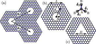
The unit cell of an antidot lattice with a triangular perforation, which can be characterized by (where is the side length of the triangle), is shown in Fig. 1(c). The number of carbon atoms (hereafter C atoms) per unit cell of an antidot lattice will henceforth be denoted by .
If we take a C atom on sublattice A at the origin, its nearest neighbors are determined by vectors , , and (see Fig. 1). Alternatively, for a C atom on sublattice B at origin, the corresponding vectors are ,, and .
II.2 Method for band-structure calculation
Given the large size of the unit cells in our superlattice – that in the cases of practical interest, with antidot diameter larger than about nm, have numbers of C atoms in excess of several thousands – a band-structure calculation using the standard ab-initio methods based on the density functional theory (DFT) is not feasible. We thus compute the electronic band structure of graphene antidot lattices within a -orbital tight-binding model. This method is known to reproduce very accurately the low-energy part of the DFT band structure of pristine graphene. Reich et al. (2002)
The tight-binding Hamiltonian of an antidot lattice reads
| (1) |
where vectors designate unit cells (in total of them), () specify positions of C atoms within a unit cell, stands for nearest neighbors of a C atom at position , and eV is the nearest-neighbor hopping matrix element, while the factor is needed to correct for double-counting. After Fourier transformation to momentum-space, the band-structure calculation amounts to a sparse-matrix diagonalization problem of dimension .
The Bloch wave functions corresponding to the energy eigenvalues are given by , where . Here enumerates energy bands (with possible additional degeneracy labelled by ) and denotes the orbital of a C atom. The energy eigenvalue problem reduces to , with matrices and given by and , respectively. In the nearest-neighbor approximation
| (2) |
where the summation runs over superlattice vectors , , (only neighboring unit cells contribute), and if C atoms at positions and are nearest neighbors, while otherwise. To a good approximation, the overlap of orbitals on different C atoms can be neglected, so that . This is a standard practice in the analyses of -electron systems. Hannewald et al. (2004)
For later reference, we describe a construction of an orthonormal eigenbasis of . To that end, we first note that form an orthonormal set: . [For the orthogonality follows from , while for it holds because and belong to different eigensubspaces of the lattice-translation operator.] This implies that for . Therefore, to construct an orthonormal set, we find an orthonormal basis in the degenerate eigensubspaces of . The orthogonality of the latter basis implies that .
II.3 Tunneling current distribution
STM and related techniques are known as powerful tools for mapping out the spatial form of surface electron states. Binnig and Rohrer (1999) In order to visualize the spatial structure of the studied low-energy states and provide the means of comparing our results to STM measurements, we predict the tunneling current distribution.
The tunneling current
| (3) |
with being the Fermi energy and the STM-tip bias voltage, can be used to probe the spatial dependence of the local density of states Gro
| (4) |
This is a basis-independent quantity, expressed here in terms of an orthonormal eigenbasis of , constructed as described above. In the case that only one flat band at falls into the energy window in Eq. (3), we have
| (5) |
Strictly speaking, to calculate the tunneling current we would need to use the explicit form of orbitals. However, Eq. (5) simplifies if we assume that the orbitals are well-localized on C atoms and hence neglect the overlap of the neighboring orbitals. After coarse-graining in the vicinity of a C atom positioned at , we obtain the sought-after tunneling current distribution
| (6) |
which is a lattice-periodic quantity.
III Results and Discussion
In this section, we investigate the band structure of antidot lattices, with emphasis on localized states at low energy. The spatial profile of these states is characterized by a tunneling current distribution. We present results for both ideal lattices and lattices with defects (vacancies and/or debonded C atoms). Since we describe the system by a nearest-neighbor tight-binding model on a bipartite lattice, the resulting energy spectrum has particle-hole symmetry. Faz With this in mind, in the following we focus on the bands above or at the Fermi level ().
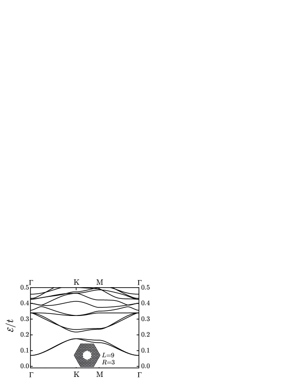
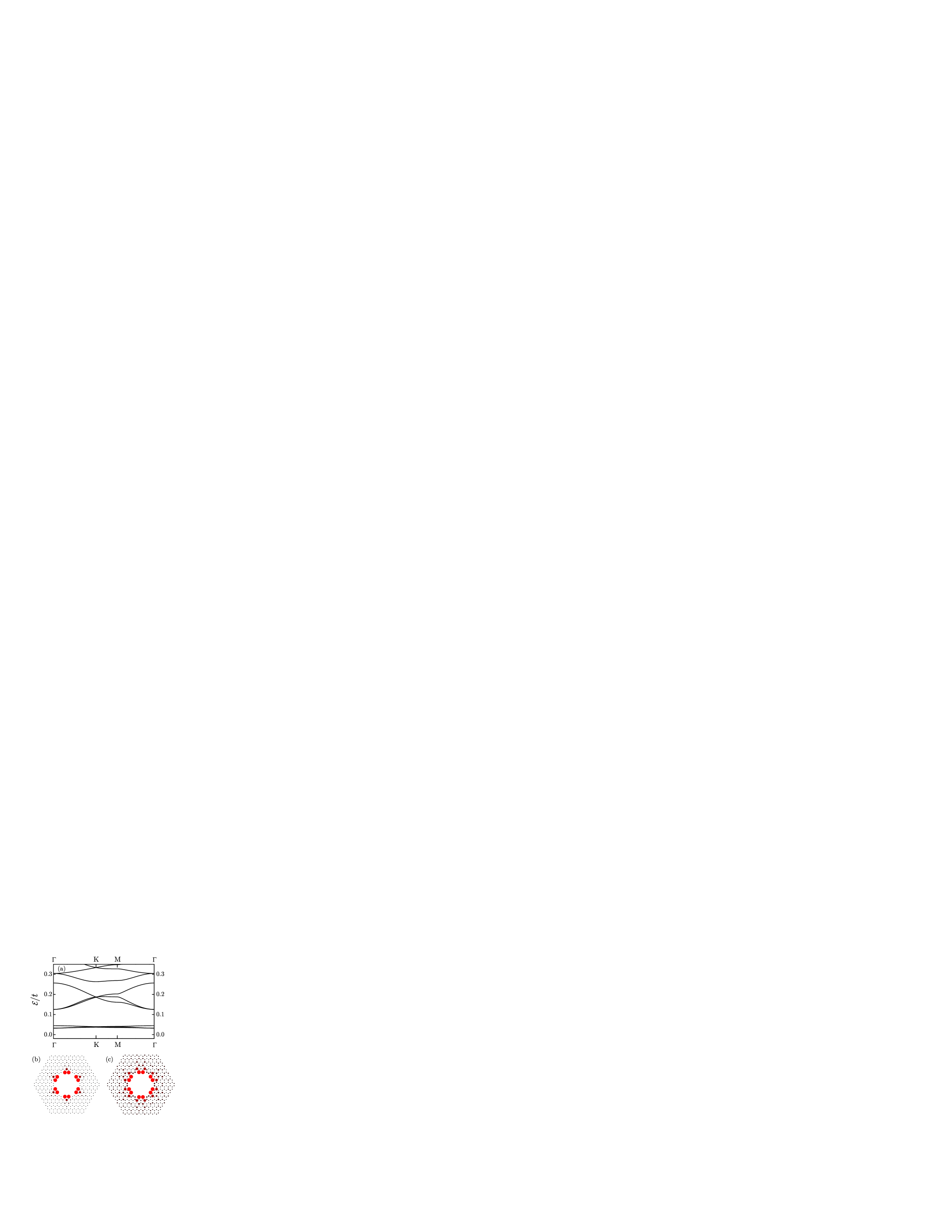
We start with an antidot lattice that is made up of perfect circular perforations, such as those considered in Ref. Pedersen et al., 2008a. The band-structure of an antidot lattice is shown in Fig. 2. A band gap opens at the -point (). For antidot lattices with a relatively small number of removed C atoms () compared to the total number of atoms in the original unit cell (), the band gap has been predicted to scale as Pedersen et al. (2008a) . It has been demonstrated that localized states with energy inside the gap can be induced in this system by defects on the superlattice scale, e.g., missing circular antidots in the lattice. Pedersen et al. (2008a) Such localized states have been proposed as hosts for local spin moments that may be utilized for quantum computation. In the following, we show that these midgap states appear generically in graphene antidot lattices, even without superlattice-scale defects.
In the nearest-neighbor approximation, graphene has a bipartite lattice, that is, a lattice that can be divided into two sublattices, A and B, where only sites at different sublattices are connected through nonzero hopping matrix elements. Inui et al. Inui et al. (1994) showed that in such systems one has zero-energy states, where are the total number of sites on the respective sublattices. [This result was, in fact, implicitly known even earlier: it was obtained by Lieb Lieb (1989) as a prerequisite for the proof that the total spin in the exact ferromagnetic ground state of the Hubbard model on a bipartite lattice is .] In a graphene superlattice with and sites per unit cell on the A- and B-sublattices, respectively, these states form dispersionless (flat) bands at . A sublattice imbalance is generically introduced at the edges of graphene-based structures. Perhaps the most well-known example of the corresponding zero energy states are the edge states in zigzag graphene ribbons that form a partially flat band at the Dirac point. Fujita et al. (1996); Nakada et al. (1996) A pair of essentially flat (spin-polarized) bands close to the Fermi level was found also in a hydrogenated graphene ribbon, as demonstrated by ab-initio electronic structure calculations. Kusakabe and Maruyama (2003)
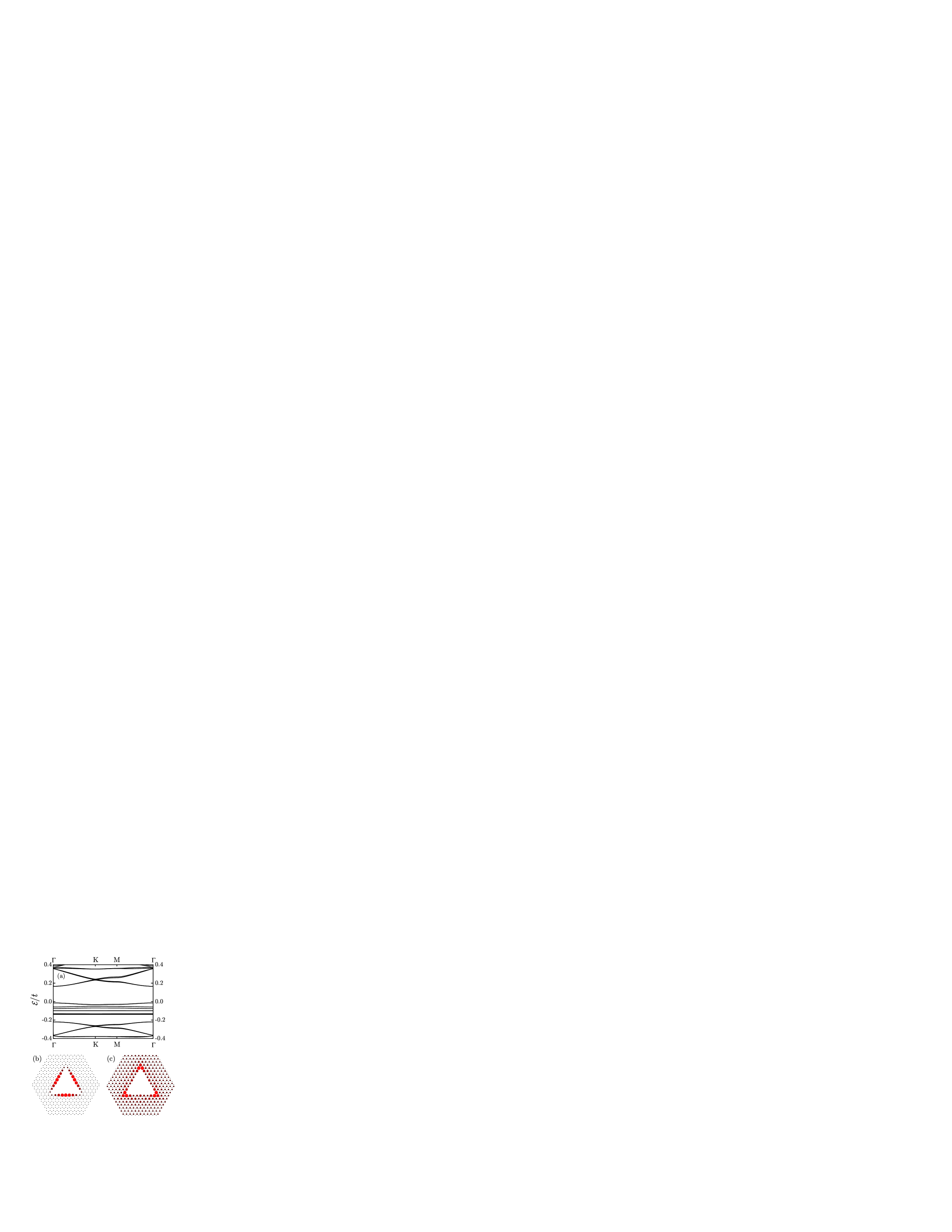
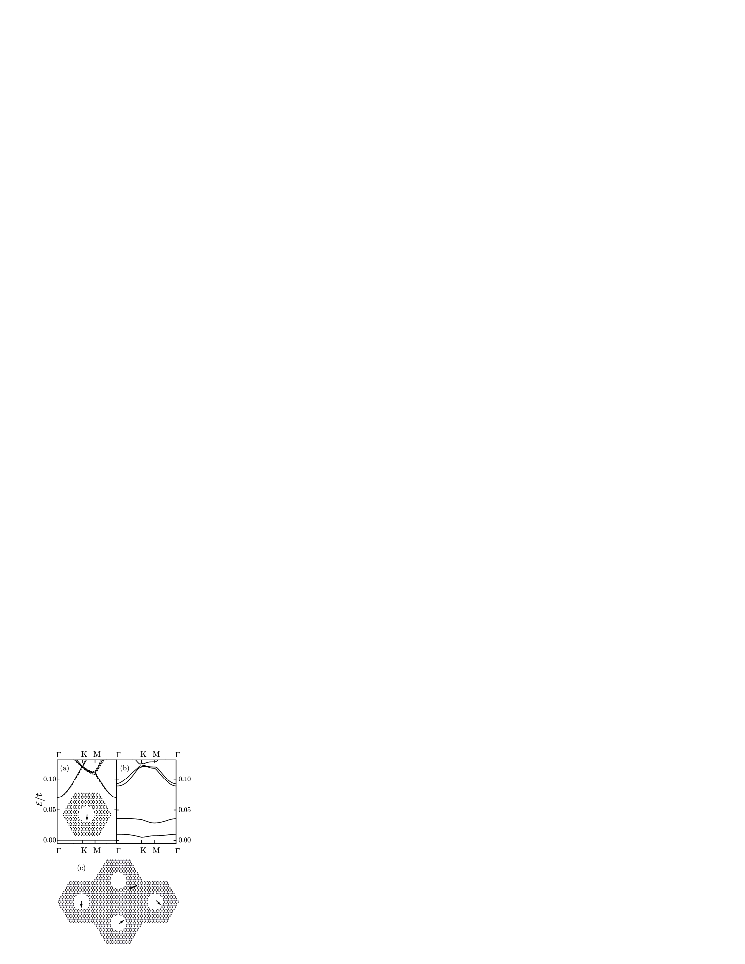
In antidot lattices one expects flat bands at zero energy due to sublattice imbalances along the edges of the antidots. The sublattice imbalance can occur even for perfect regularly shaped antidots. As an example, we study antidot lattices with triangular perforations (cf. Fig. 1), which invariably have an imbalance of per antidot. Consequently, a -fold degenerate flat band emerges at , as depicted in Fig. 3. On the other hand, it is easy to check that antidot lattices with perfect circular perforations always have . These lattices therefore do not exhibit flat bands at (cf. Fig. 2).

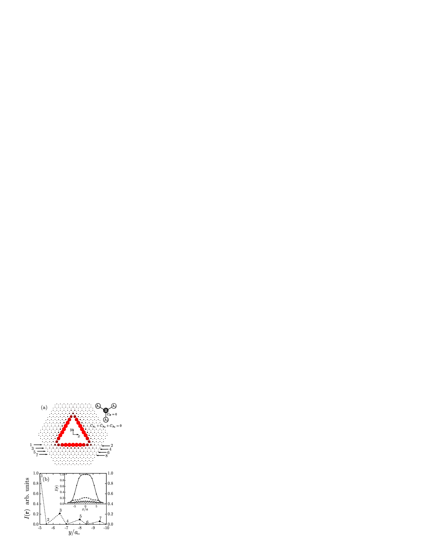
As pointed out by Inui et al.,Inui et al. (1994) the single-particle states corresponding to the zero energy flat bands are pseudospin-polarized – they occupy only sites belonging to a particular sublattice. Figure 4 shows for an antidot lattice how this effect manifests itself in the tunneling current distribution, which is proportional to the on-site electron density. Closer inspection reveals that the single-particle states corresponding to the flat band at indeed leave the B-sublattice sites unoccupied (amplitudes ), while the A-sublattice sites are occupied with amplitudes (normalized as ), adding up to zero around each B-sublattice site [see Fig. 4(a)]. Moreover, the electronic states corresponding to the zero-energy flat bands are predominantly localized in the vicinity of the antidot edge. Jaf The extent of their spatial localization is illustrated in Fig. 4(b).
It is important to emphasize that the above results are valid for an arbitrary system of bipartite structure, either infinite or of finite size, and even in the presence of off-diagonal disorder and/or an external magnetic field. Inui et al. (1994) (In the presence of a magnetic field, the hopping matrix elements become complex through the conventional Peierls substitution Peierls (1933) and the particle-hole symmetry is destroyed.) Therefore, even without actual calculation, we can conclude that the discussed flat bands at in graphene antidot lattices remain flat in a magnetic field. Analogous results for finite-size graphene antidot flakes have recently been obtained numerically. Bahamon et al. (2009)
A different perspective on the problem is furnished by a symmetry-based classification of superhoneycomb systems, as put forward by Shima and Aoki. Shima and Aoki (1993) They showed that such systems can have either semiconducting (with direct band gap), semimetallic, or metallic character. This classification turns out to depend not only on the global superlattice symmetry, but also on the specific atomic configuration within the unit cell. In particular, structures with , , , and ( is an integer) atoms per unit cell belong to symmetry classes designated by , , , and , respectively. Shima and Aoki (1993) The respective degeneracies of the flat bands at in these classes are , , , and ( is an integer). According to this classification, our antidot lattices with circular perforations belong to the -type of superhoneycomb systems with , which is consistent with the absence of flat bands at .
In realistic graphene flakes, the dangling bonds along the edges are hydrogen-passivated, giving rise to an on-site potential. An on-site potential can also appear in a pure carbon system, due to a weak edge-magnetization induced by electron-electron interactions. Edg Since the electronic states corresponding to the zero-energy flat bands are largely localized at the antidot edges, one expects them to be strongly affected by such an edge potential. This motivates us to study the influence of an edge potential, hereafter denoted by , on the zero-energy states. We assume that takes nonzero values at C atoms that have only two nearest neighbors. Such a potential breaks the particle-hole symmetry of the energy spectrum by destroying the bipartite lattice structure, since it couples sites that belong to the same sublattice. However, the main effect of is a lifting of the degeneracy of the zero-energy flat bands, while their dispersionless character is largely being preserved. com At the same time, the effect of this potential on the other bands is relatively small [cf. Figs. 5(a) and 3(b)]. This finding is indeed analogous to the behavior of flat bands in nanoribbons with hydrogenated edges, obtained using realistic first-principles DFT calculations. Kusakabe and Maruyama (2003) We stress that the observed effect of the on-site potential is robust, i.e., changing the magnitude of does not alter our qualitative conclusions.
In what follows, we point out another generic feature of graphene antidot lattices: the occurrence of essentially flat bands at nonzero energies (even in the absence of an edge potential, ). A characteristic example is presented in Fig. 6. While flat bands at in bipartite lattices arise due to a global sublattice imbalance (), as discussed above, we ascribe the quasi-flat ones at to local sublattice imbalances (while globally ). Such local imbalances can be induced even in regularly shaped antidot lattices, for instance, by debonded C atoms with a single neighbor at the edges [cf. Fig. 6(b)].
The occurrence of quasi-flat bands may be understood as follows. A single debonded C atom induces a sublattice imbalance that leads to a zero energy “defect level”. One may view a collection of debonded C atoms as a collection of “local sublattice imbalances” that induce one defect level each with wave functions that are localized in the vicinity of the defects. This picture is supported by the tunneling density of states shown in Fig. 6(b). Localized states induced by defects that are well separated from one another hybridize only weakly. Accordingly, these defect levels give rise to essentially dispersionless bands close to the Fermi level (). Jpn As the distance between the defects decreases, the hybridization of defect states becomes stronger and the resulting bands are shifted away from the Fermi level.
In disordered antidot lattices, debonded C atoms generically appear along the edges of irregularly shaped antidots, leading to a local sublattice imbalance. Such defects at the edge of a zigzag nanoribbon have been experimentally observed quite recently. Liu et al. (2009) In this experiment, the multilayer graphene structures were thermally-treated leading to edges that are mostly closed (i.e., folded from one layer to another). Open-edge structures with debonded C atoms are found in a local area where the folding edge is partially broken. Another source of local sublattice imbalances in disordered lattices are vacancies, for example, due to removed C atoms or C atoms that are rehybridized as a result of hydrogen chemisorption. Mizes and Foster (1989); Ruffieux et al. (2000); Rutter et al. (2007) In Fig. 7(a), we show that a single defect in an otherwise perfectly circular antidot lattice produces, as expected, a zero-energy band. Needless to say, in realistic disordered systems defects do not repeat with the lattice period as assumed in Fig. 7(a). Some qualitative features of realistic disordered lattices can be captured by considering a superlattice with an increased unit cell. In Fig. 7(b), we show a band structure for an antidot lattice with a unit cell containing four antidots with defects at different locations; this band structure indicates that well-separated defect states weakly hybridize, giving rise to two pairs of quasi-flat bands that are symmetric with respect to the Fermi level. This suggests that for realistic disordered lattices one has a quasicontinuum of such low-energy states due to hybridization of defect states.
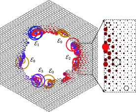
We finally consider an antidot lattice with strong shape irregularities, as is likely the case in current experiments. Shen et al. (2008); Eroms and Weiss Although our calculation, the result of which is shown in Fig. 8, is based on periodically repeated defects, we expect that it will give reliable estimates for the localization properties of the appearing midgap states. The localization length found in this manner can be used to estimate the charging energy in the system. The obtained band structure has the expected features: the number of flat bands at is in agreement with general result for the bipartite systems, and the quasi-flat bands at nonzero energies correspond to local sublattice imbalances. The electron states for both types of flat bands are localized in the vicinity of the zigzag-like segments of the antidot edges and debonded C atoms, as illustrated in Fig. 8. (In contrast to the zigzag-like segments, their armchair-like counterparts on the antidot edges do not exhibit electron localization.) Moreover, the tunneling current is maximal at the midpoints of the zigzag-like segments on the antidot edges. These features are in agreement with the existing experimental results on stepped graphite surfaces, Kobayashi et al. (2006) which have edges with similar irregularities.
Also depicted in Fig. 8 (see the zoomed part) is a “charge-density reconstruction” from the original graphene honeycomb lattice into a lattice with times larger period, which is rotated by an angle of . This is a manifestation of a Friedel-oscillation-like phenomenon, that is, a long-range electronic perturbation caused by the presence of defects. Such interference phenomena, which are essentially a consequence of the wave nature of electrons, are familiar in the context of impurities on surfaces of metals Hasegawa and Avouris (1993) and were observed on the graphite and graphene surfaces using STM. Mizes and Foster (1989); Mallet et al. (2007) In the case of graphene, the charge-density reconstruction results from intervalley coupling of the electronic -states. We thus conclude that there is strong intervalley scattering at the antidot edges in the lattice shown in Fig. 8. This is in agreement with the experiments of Refs. Shen et al., 2008 and Eroms and Weiss, , where the observed weak localization (instead of weak antilocalization) is a signature of intervalley scattering at the antidot edges.
The numerically obtained localization of the induced midgap states at the antidot edges, with a localization length on the order of a few interatomic distances, suggests that the charging energies for these states can be substantial. Assuming completely random edges of length , one expects low-energy states per unit cell due to local sublattice imbalances (in a realistic disordered system these states will not be strictly at zero energy since the local sublattice imbalances in individual unit cells will partially cancel between unit cells). For the parameters in the experiment of Ref. Eroms and Weiss, , one thus expects a spacing between these localized states of about along the edge, implying a charging energy that is substantially larger than the band gap in the system, which is roughly inversely proportional to the distance between antidots. Also, since the low-energy edge states due to local sublattice imbalances are separated by the antidot distance, one expects that their energy after hybridization is at most on the order of the band gap. Figure 7 supports this estimate. We thus conclude that the localized states observed in Fig. 8 have kinetic energies inside the band gap of the perfectly regular lattice, but charging energies that by far exceed that band gap. This suggests that local spin moments may form at the edges of disordered antidot lattices at Fermi energies where charge transport takes place. Since local magnetic moments are known to be an effective source of electron dephasing in weak localization experiments, dep the studied midgap states offer an alternative explanation for the saturation of the electron dephasing length at a scale corresponding to the distance between antidots reported in Ref. Eroms and Weiss, .
IV Conclusions
In this work, we have studied the salient features of the low-energy band structure of graphene antidot lattices. Apart from strictly zero-energy (midgap) flat bands that arise from the bipartite lattice structure and a global sublattice imbalance, we have also found quasi-flat bands at low, but nonzero, energies that can be ascribed to local sublattice imbalances. In addition, we have examined the influence of an edge potential on the flat bands, showing that such a potential lifts the degeneracy of these bands, without affecting significantly their dispersionless character.
We have also investigated the spatial profile of the electronic states corresponding to both classes of low-energy bands (flat and quasi-flat). By analyzing the tunneling-current distributions that can be compared to STM measurements, we have demonstrated that these electronic states are generically localized at the antidot-edges. The computed tunneling current distributions also show a charge-density reconstruction from the original honeycomb lattice to a lattice with times larger period and rotated through an angle of . This phenomenon is indicative of intervalley scattering off irregular antidot edges, as also observed in recent experiments. Shen et al. (2008); Eroms and Weiss
The spatial profiles of the localized midgap states that we find allow for a rough estimate of their charging energies. That estimate suggests that such states can host local magnetic moments. We propose that such magnetic moments may be at the origin of a recently observed saturation of the dephasing length in graphene antidot lattices. Eroms and Weiss In addition, the investigated midgap states compete with the localized states due to superlattice-scale defects, and therefore can have significant implications for a recent proposal of spin qubits in graphene antidot lattices.Pedersen et al. (2008a)
Acknowledgements
We acknowledge a helpful correspondence with J. Eroms and discussions with C. Flindt.
References
- Gra (a) For a review, see A. H. Castro Neto, F. Guinea, N. M. R. Peres, K. S. Novoselov, and A. K. Geim, Rev. Mod. Phys. , 109 (2009).
- Novoselov et al. (2004) K. S. Novoselov, A. K. Geim, S. V. Morozov, D. Jiang, Y. Zhang, S. V. Dubonos, I. V. Grigorieva, and A. A. Firsov, Science 306, 666 (2004).
- Zhou et al. (2007) S. Y. Zhou, G. H. Gweon, A. V. Fedorov, P. N. First, W. A. de Heer, D. H. Lee, F. Guinea, A. H. Castro Neto, and A. Lanzara, Nat. Mater. 6, 770 (2007).
- Wu et al. (2007) X. Wu, X. Li, Z. Song, C. Berger, and W. A. de Heer, Phys. Rev. Lett. 98, 136801 (2007).
- Zhou et al. (2008) S. Y. Zhou, D. A. Siegel, A. V. Fedorov, F. El Gabaly, A. K. Schmid, A. H. Castro Neto, and A. Lanzara, Nat. Mater. 7, 259 (2008).
- Tworzydlo et al. (2006) J. Tworzydlo, B. Trauzettel, M. Titov, A. Rycerz, and C. W. J. Beenakker, Phys. Rev. Lett. 96, 246802 (2006).
- Peres et al. (2006) N. M. R. Peres, A. H. Castro Neto, and F. Guinea, Phys. Rev. B 73, 195411 (2006).
- (8) Y. W. Son, M. L. Cohen, and S. G. Louie, Phys. Rev. Lett. , (2006); M. Wimmer, I. Adagideli, S. Berber, D. Tománek, and K. Richter, ibid. , (2008).
- Cheianov and Fal’ko (2006) V. V. Cheianov and V. I. Fal’ko, Phys. Rev. B 74, 041403 (2006).
- Katsnelson et al. (2006) M. I. Katsnelson, K. S. Novoselov, and A. K. Geim, Nature Phys. 2, 620 (2006).
- (11) E. H. Hwang, S. Adam, and S. Das Sarma, Phys. Rev. Lett. , (); E. H. Hwang and S. Das Sarma, Phys. Rev. B , ().
- Trauzettel et al. (2007) B. Trauzettel, D. V. Bulaev, D. Loss, and G. Burkard, Nature Phys. 3, 192 (2007).
- Milton Pereira et al. (2007) J. Milton Pereira, P. Vasilopoulos, and F. M. Peeters, Nano Lett. 7, 946 (2007).
- Recher et al. (2007) P. Recher, B. Trauzettel, A. Rycerz, Y. M. Blanter, C. W. J. Beenakker, and A. F. Morpurgo, Phys. Rev. B 76, 235404 (2007).
- Stauber et al. (2008) T. Stauber, N. M. R. Peres, and A. H. Castro Neto, Phys. Rev. B 78, 085418 (2008).
- (16) G. W. Semenoff, Phys. Rev. Lett. , (); D. P. DiVincenzo and E. J. Mele, Phys. Rev. B , ().
- Beenakker (2008) C. W. J. Beenakker, Rev. Mod. Phys. 80, 1337 (2008).
- Stander et al. (2009) N. Stander, B. Huard, and D. Goldhaber-Gordon, Phys. Rev. Lett. 102, 026807 (2009).
- Gra (b) A. Rycerz, J. Tworzydlo, and C. W. J. Beenakker, Nat. Phys. , 172 (2007); L. A. Ponomarenko, F. Schedin, M. I. Katsnelson, R. Yang, E. W. Hill, K. S. Novoselov, and A. K. Geim, Science , (); X. Du, I. Skachko, and E. Y. Andrei, Phys. Rev. B , (2008); V. M. Pereira and A. H. Castro Neto, arXiv:0810.4539v1 (unpublished).
- Wang et al. (2008) X. Wang, Y. Ouyang, X. Li, H. Wang, J. Guo, and H. Dai, Phys. Rev. Lett. 100, 206803 (2008).
- Lin et al. (2009) Y.-M. Lin, K. A. Jenkins, A. Valdes-Garcia, J. P. Small, D. B. Farmer, and P. Avouris, Nano Lett. 9, 422 (2009).
- (22) For a review, see P. Avouris, Z. Chen, and V. Perebeinos, Nat. Nanotechnol. , 605 (2007).
- (23) C. Berger et al., Science 312, 1191 (2006); M. D. Fischbein and M. Drndić, Appl. Phys. Lett. 93, 113107 (2008).
- Molitor et al. (2007) F. Molitor, J. Güttinger, C. Stampfer, D. Graf, T. Ihn, and K. Ensslin, Phys. Rev. B 76, 245426 (2007).
- Giesbers et al. (2008) A. J. M. Giesbers, G. Rietveld, E. Houtzager, U. Zeitler, R. Yang, K. S. Novoselov, A. K. Geim, and J. C. Maan, Appl. Phys. Lett. 93, 222109 (2008).
- Ki et al. (2008) D.-K. Ki, D. Jeong, J.-H. Choi, H.-J. Lee, and K.-S. Park, Phys. Rev. B 78, 125409 (2008).
- Geim and Novoselov (2007) A. K. Geim and K. S. Novoselov, Nat. Mater. 6, 183 (2007).
- Han et al. (2007) M. Y. Han, B. Özyilmaz, Y. Zhang, and P. Kim, Phys. Rev. Lett. 98, 206805 (2007).
- Lin et al. (2008) Y.-M. Lin, V. Perebeinos, Z. Chen, and P. Avouris, Phys. Rev. B 78, (R) (2008).
- Stampfer et al. (2009) C. Stampfer, J. Güttinger, S. Hellmüller, F. Molitor, K. Ensslin, and T. Ihn, Phys. Rev. Lett. 102, 056403 (2009).
- Russo et al. (2008) S. Russo, J. B. Oostinga, D. Wehenkel, H. B. Heersche, S. S. Sobhani, L. M. K. Vandersypen, and A. F. Morpurgo, Phys. Rev. B 77, 085413 (2008).
- Pedersen et al. (2008a) T. G. Pedersen, C. Flindt, J. Pedersen, N. A. Mortensen, A.-P. Jauho, and K. Pedersen, Phys. Rev. Lett. 100, 136804 (2008a).
- Pedersen et al. (2008b) T. G. Pedersen, C. Flindt, J. Pedersen, A.-P. Jauho, N. A. Mortensen, and K. Pedersen, Phys. Rev. B 77, 245431 (2008b).
- Shen et al. (2008) T. Shen, Y. Q. Wu, M. A. Capano, L. R. Rokhinson, L. W. Engel, and P. D. Ye, Appl. Phys. Lett. 93, 122102 (2008).
- (35) J. Eroms and D. Weiss, arXiv:0901.0840v1 (unpublished).
- Yazyev (2008) O. V. Yazyev, Phys. Rev. Lett. 101, 037203 (2008).
- (37) J. J. Palacios, J. Fernández-Rossier, and L. Brey, Phys. Rev. B , (); J. Fernández-Rossier and J. J. Palacios, Phys. Rev. Lett. , ().
- (38) S. Hikami, A. I. Larkin, and Y. Nagaoka, Prog. Theor. Phys. , 707 (1980); F. Pierre and N. O. Birge, Phys. Rev. Lett. , 206804 (2002).
- Lieb (1989) E. H. Lieb, Phys. Rev. Lett. 62, 1201 (1989).
- Inui et al. (1994) M. Inui, S. A. Trugman, and E. Abrahams, Phys. Rev. B 49, 3190 (1994).
- Shima and Aoki (1993) N. Shima and H. Aoki, Phys. Rev. Lett. 71, 4389 (1993).
- Reich et al. (2002) S. Reich, J. Maultzsch, C. Thomsen, and P. Ordejón, Phys. Rev. B 66, 035412 (2002).
- Hannewald et al. (2004) K. Hannewald, V. M. Stojanović, J. M. T. Schellekens, P. A. Bobbert, G. Kresse, and J. Hafner, Phys. Rev. B 69, 075211 (2004).
- Binnig and Rohrer (1999) G. Binnig and H. Rohrer, Rev. Mod. Phys. 71, S324 (1999).
- (45) See, for example, G. Grosso and G. P. Parravicini, Solid State Physics (Academic Press, New York, 2003), p. 20.
- (46) See, for example, P. Fazekas, Lecture Notes on Electron Correlation and Magnetism (World Scientific, New York, 1999).
- Fujita et al. (1996) M. Fujita, K. Wakabayashi, K. Nakada, and K. Kusakabe, J. Phys. Soc. Jpn. 65, 1920 (1996).
- Nakada et al. (1996) K. Nakada, M. Fujita, G. Dresselhaus, and M. S. Dresselhaus, Phys. Rev. B 54, 17954 (1996).
- Kusakabe and Maruyama (2003) K. Kusakabe and M. Maruyama, Phys. Rev. B 67, 092406 (2003).
- (50) Similar midgap states have recently been shown to lead to an order-of-magnitude increase in conductance in graphene; see S. Jafri et al., arXiv:0905.1346v1 (unpublished).
- Peierls (1933) R. E. Peierls, Z. Phys. 80, 763 (1933).
- Bahamon et al. (2009) D. A. Bahamon, A. L. C. Pereira, and P. A. Schulz, Phys. Rev. B 79, 125414 (2009).
- (53) This is, indeed, intuitively plausible from the point of view of the standard first-order Rayleigh-Schrödinger perturbation theory of a degenerate energy level; see, for example, L. D. Landau and E. M. Lifshitz, Quantum Mechanics, Course of Theoretical Physics Vol. 3 (Pergamon, Oxford, 1991).
- (54) S. Nishino, M. Goda, and K. Kusakabe, J. Phys. Soc. Jpn. , (); S. Miyahara, K. Kubo, H. Ono, Y. Shimomura, and N. Furukawa, ibid. , (2005).
- Liu et al. (2009) Z. Liu, K. Suenaga, P. J. F. Harris, and S. Iijima, Phys. Rev. Lett. 102, 015501 (2009).
- Mizes and Foster (1989) H. A. Mizes and J. S. Foster, Science 244, 559 (1989).
- Ruffieux et al. (2000) P. Ruffieux, O. Gröning, P. Schwaller, L. Schlapbach, and P. Gröning, Phys. Rev. Lett. 84, 4910 (2000).
- Rutter et al. (2007) G. M. Rutter, J. N. Crain, N. P. Guisinger, T. Li, P. N. First, and J. A. Stroscio, Science 317, 219 (2007).
- Kobayashi et al. (2006) Y. Kobayashi, K.-I. Fukui, T. Enoki, and K. Kusakabe, Phys. Rev. B 73, 125415 (2006).
- Hasegawa and Avouris (1993) Y. Hasegawa and P. Avouris, Phys. Rev. Lett. 71, 1071 (1993).
- Mallet et al. (2007) P. Mallet, F. Varchon, C. Naud, L. Magaud, C. Berger, and J.-Y. Veuillen, Phys. Rev. B 76, 041403(R) (2007).