Origin of Ferroelastic Domains in Free-Standing Single Crystal Ferroelectric Films
Abstract
The origin of the unusual 90°ferroelectric / ferroelastic domains, consistently observed in recent studies on meso and nanoscale free-standing single crystals of BaTiO3 [Schilling et al., Physical Review B, 74, 024115 (2006); Schilling et al., Nano Letters, 7, 3787 (2007)], has been considered. A model has been developed which postulates that the domains form as a response to elastic stress induced by a surface layer which does not undergo the paraelectric-ferroelectric, cubic-tetragonal phase transition. This model was found to accurately account for the changes in domain periodicity as a function of size that had been observed experimentally. The physical origin of the surface layer might readily be associated with patterning damage, seen in experiment; however, when all evidence of physical damage is removed from the BaTiO3 surfaces by thermal annealing, the domain configuration remains practically unchanged. This suggests a more intrinsic origin, such as the increased importance of surface tension at small dimensions. The effect of surface tension is also shown to be proportional to the difference in hardness between the surface and the interior of the ferroelectric. The present model for surface tension induced twinning should also be relevant for finely grained or core-shell structured ceramics.
pacs:
77.80.Bh, 77.55.+f, 77.80.DjIntroduction
In 1935 Landau and Lifshitz predicted the appearance of periodic, thermodynamically stable, domains, with oppositely oriented magnetic moments, in ferromagnetic crystals. The existence of these domains minimized the energy of the depolarizing field, caused by the abrupt discontinuity of the spontaneous magnetization at the sample surface Landau1935 . Additional consideration of the associated domain wall energies allowed them to predict a square root dependence of the domain period on the sample thickness. This square root relationship is often referred to as the Kittel law because of its independent formulation in 1946 by Kittel Kittel1946 . The law is also valid for 180°domains in ferroelectric crystals Mitsui1953 ; Streiffer2002 , where the unfavourable depolarizing electric field is provided by the abrupt polar discontinuity at the surface. The Landau-Lifshitz-Kittel theory was later extended by Roytburd Roytburd1976 to describe the behaviour of ferroelastic domains formed as a result of substrate clamping effects in thin film systems.
In previous studies we have shown that the Kittel law works perfectly for a wide class of ferroic materials (ferromagnetic, ferroelectric or ferroelastic) over six orders of magnitude in film thickness Scott2006 ; Schilling2006 , and that it can be intuitively expressed in terms of the domain wall thickness Catalan2007 ; Stephanovich2005 ; Guerville2005 . Moreover, we have demonstrated that the Kittel approach can be extended to three dimensional structures Schilling2006b ; Catalan2007b ; Schilling2007 , to ferroelectric superlattices Stephanovich2005 and to multiferroic materials Catalan2008 ; Daraktchiev2008 . Much of the experimental work has been in association with observations of periodic 90°ferroelectric-elastic domains that have been consistently observed in free-standing single crystal thin films (see Fig.1a) and nanowires of BaTiO3. In all our experiments, the size of the 90°domains as a function of size is indeed found to be well described by a Kittel-Roytburd formalism.
At first glance, however, the very existence of such domains in our free-standing samples is quite surprising. Ferroelastic domains normally appear in response to an external stress (such as that imposed by clamping to a rigid substrate, for example) which forces the sample towards shape preservation in the clamped directions. The domain configuration is such that the macroscopic shape difference between the paraphase and the ferrophase is minimized, while the domain size responds to an equilibrium between domain energy and domain wall energy Roytburd1976 . However, our BaTiO3 lamella are free standing single crystals and therefore free from epitaxially-induced stress, so they have no Roytburd-like interface-induced elastic driving force. The question, then, is the following: if there is no external stress, what causes the appearance of the ferroelastic domains?
In the present work we explain the appearance of the self-organized domain patterns in free-standing nano-samples of BaTiO3 by assuming that the driving stress is provided by an encapsulating surface layer. In much of our experimental work, this encapsulation layer could easily be associated with the surface damage caused by focused ion beam milling. However, we have also observed here that 90°domains persist, with only slightly altered periodicities, even when surface damage has been repaired by thermal annealing; this suggests that the strain effects may in fact arise intrinsically from surface tension, being therefore unavoidable even in nominally ”perfect” free-standing ferroelectric nanostructures.
(a)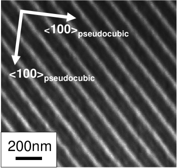
(b)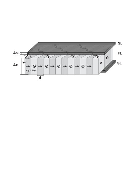
Model
The development of the model focuses on the geometry of the single crystal lamellae first reported in ref.Schilling2006 , an example of which is shown in Figure 1(a). Figure 1 (b) shows a schematic cross-section of our model representation for such BaTiO3 lamella, with the surface encapsulation layers (SL’s) that are potentially responsible for the formation of 90°domains present and their obeyance to Kittel behaviour. The model comprises a tetragonal ferroelectric/ferroelastic layer (FL) of thickness , exemplified by BaTiO3, sandwiched between two cubic paraelectric surface layers (SL) of thickness . The surface layers provide the stress for the creation of the ferroelectric-ferroelastic domains in the FL. The assumption of cubic surfaces is supported by the observation that barium titanate nanoparticles have a core-shell structure with tetragonal interior and cubic surfaces Takeuchi1994 ; Tanaka1998 . However, the cubic symmetry is not a key feature of the model: for the SL to impose stress on the interior, it is just sufficient that it does not undergo the phase transition at . A non-ferroelectric capsule/matrix was also assumed in recent phase-field simulations of domain patterns in ferroelectric nanostructuresSlutsker2008 .
In the present model, the SL thickness is an adjustable parameter to be determined from experimental measurements. The cartesian z-axis is oriented perpendicular to the plane of the lamella, and the x and y axes coincide with the crystal axes of BaTiO3 as shown in Fig. 1a. The equilibrium lattice parameters of the FL are assumed to be those of the bulk ferroelectric tetragonal BaTiO3 crystal and, in order to minimize depolarization fields, the polarization will tend to lie within the XY plane, pointing parallel to either the X or Y directions. In terms of notation, [] if is parallel to or [] if is parallel to . The formation of the SL with different equilibrium lattice constants [] results in elastic stress, provided by lattice matching at the FL and SL interface.
Consider to start with the simplest possibility when the matching stress is uniform, i.e., there are no stress gradients. Because SL is much thinner than FL, the latter remains undeformed, keeping the equilibrium BaTiO3 lattice parameters ([] or []). Deformation concerns only the SL which, because of the matching conditions, should conserve the same XY-plane parameters as the FL but can relax in the Z direction (). The corresponding deformation energy is caused by the in-plane misfit strains of SL and contains the tension and shear parts Pompe1993 ; Speck1994 ; Speck1995 ; Pertsev1995 :
| (1) | |||||
where the diagonal components of the plain strain tensor of SL are expressed via the mismatch parameters:
| (2) |
is the shear modulus, is the Poisson ratio and the factor 2 corresponds to two (top and bottom) SLs on both sides of FL. We assume that Cheng1996 and Bradfield1950 are approximately the same for SL and FL.
Such system can be unstable towards formation of the experimentally observed periodic structure of 90°ferroelastic domains shown in Fig. 1. Usually, such domains have 45°domain walls and ”head-to-tail” polarization contacts to avoid the formation of depolarization charge. The reason of the instability is that domain formation can reduce the elastic energy (1) of the SL by allowing the misfit stress to gradually relax inside the FL, within an interfacial region whose thickness is of the order of the domain width . The domains will appear when the elastic energy imposed onto the SL by the ferroelectric is bigger than the energy required for the formation of domain walls. We emphasize that, although the net effect of ferroelastic twinning is to minimize the macroscopic deformation of the SL, this twinning necessarily requires a strain gradient near the interface. This is because, while afar away from the interface the lattice parameters of the FL are those of the bulk ferroelectric, at the interface they must become closer to cubic in order to match the SL. Accordingly, an inhomogeneously strained region must appear for which flexoelectric effects may be important (Cross2006 ; Catalan2004 ; Catalan2005 ; Sharma2009 ). The flexoelectric contribution, however, has been left out of this model for the sake of simplicity.
The situation described here is in fact quite similar to the appearance of periodic 90°domains in epitaxial ferroelectric films strained by thick undeformable substrates Pompe1993 ; Speck1994 ; Pertsev1995 in which the film/substrate mismatch strain relaxes in the near-surface layer of the film. The only difference is that the contact elastic SL in our case is thin and its deformation should be considered self-consistently with that of FL. In a way, the model discussed here can be seen as a generalization of the substrate/film models for the case of a substrate that has finite thickness compared with the film.
The mechanism of nonuniform strain relaxation in the domain-populated FL gives rise to two new energy contributions: the near-surface deformation energy of the ferroelectric layer, , and the energy of the domain walls . The energy balance between , and optimizes the domain period and the matching plane lattice constants changing periodically at SL/FL interface from () at X-domain to () at Y-domain.
Before proceeding to the derivation of the total energy of the system
| (3) |
(the factors correspond to two-side SL and two-side relaxation near-surface layers in FL), we assume that the optimal domain width is thinner than FL but thicker than SL :
| (4) |
Observed in experiment and discussed in detail later, such hierarchy simplifies the calculation of the different contributions to (3).
We express the deformation energy of the ferroelectric layer in terms of periodically changing strains of domains at the surface of the FL,
| (5) |
These are taken as variational parameters in the general expression for the elastic energy of the 2-dimensional crystal, periodically strained as and with relative domain population equal to (See also Eq.(30) in Pertsev1995 ):
| (6) |
Adapting Eq.(6) to the case of equally-populated and thin domains, the universal dimensionless function can be simplified as: Pertsev1995 , and therefore:
| (7) |
Physically, the first term in (7) corresponds to the average interface-induced strain that propagates through the whole thickness of the FL. The second term is produced by the superposition of alternative strains of an infinite series of domains, compensating inside the FL and relaxing in the near-surface gradient layer of a thickness of order . Technically this sum is expressed via the zeta-function , like the electrostatic energy of alternative depolarization charge compensation in Kittel formula for ferroelectric domains Landau1935 ; Kittel1946 .
Before minimizing (7) we can ensure first the vanishing of the largest first (volume) term, selecting ; this is justified because the domain pattern can compensate for shear strains () but not for volume changes. The number of variational parameters then reduces to one: and the second (surface) term takes the form:
| (8) |
Consider now the deformation energy of the SL subjected to periodic domain-induced surface strains , taking into account that and are expressed via variational parameters and (5) as:
| (9) |
If SL is thinner than the domain structure period: the periodic surface strain does not manage to relax across the SL. Then, SL can be presented as a piecewise strained film, having uniform deformation for each section. Summing the given by the first part of Eq. (1) elastic energies from all the pieces (that are equal because of the symmetry) and taking into account the discussed above constrain we present the elastic energy of SL as a superposition of tension and shear contributions:
| (10) |
Note that the tension contribution:
| (11) |
does not depend on strain variational parameter and coincides with the tension energy of the uniformly deformed SL in (1).
Combining (8) and (10) with the energy of domain walls
| (12) |
( is the surface energy density of the domain walls), the total energy (3) is:
| (13) |
where and
| (14) |
with the length-scale parameter
| (15) |
that can be interpreted as ”domain wall half-thickness”. This value is ca. one-two lattice constants and agrees with previously reported theoretical and experimental values Zhirnov1959 ; Floquet1999 ; Vanderbilt2002 ; Shilo2004 .
Minimization of (13) over and gives the expression for optimal domain width
| (16) |
When , one can neglect the responsible for the upward curvature denominator in (16) and obtain the Kittel-type dependence (14) for . This explains why our experimental results could be reasonably well fitted assuming a simple square root dependence of domain periodicity on film thickness Schilling2006 . Note however that we are still in the thin surface layer limit . The opposite (irrelevant for our system) limit will lead to the Roytburd-Pompe-Pertsev situation of thick substrate with domain pattern also obeying the Kittel law but with a different numerical constant. When , the domain width diverges, implying a transition to a mono-domain state. Domains therefore exist only when:
| (17) |
or, taking into account (14) and (16) when:
| (18) |
where D is estimated as (15). This represents a rather narrow constraint, providing assumption (4) is satisfied.
Substitution of the optimal parameters and into (13) gives the energy of the domain state
| (19) |
which is smaller than (1) (since with ) in the limits of applicability of the theory. This confirms the instability of the ferroelectric free-standing lamella with surface tension towards domain formation.
Comparison with experiment
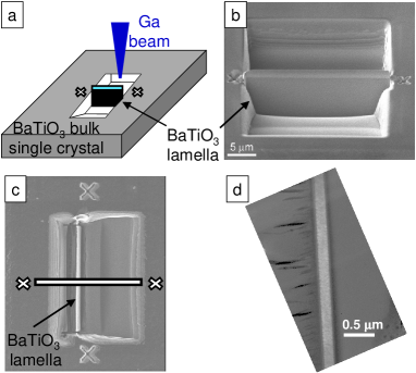
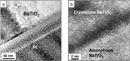
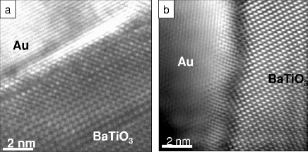
An attempt was made to use the model developed above to describe the variation in domain periodicity observed for single crystal BaTiO3 lamellae quantitatively. To do this it was noted that the previously published domain period data Schilling2006 had all been taken from lamellae for which there had been no attempt to repair surface damage caused by focused ion beam (FIB) processing. It was expected that physical ’encapsulation layers’ of amorphous BaTiO3 should exist on the top and bottom lamellar surfaces. To establish the thickness of the physically damaged layers, cross-sectional transmission electron microscopy was used, with the lamellar cross-sections prepared by FIB according to the schematic shown in figure 2. As can be seen in figure 3, a surface layer of amorphous material, approximately 20nm in thickness, was indeed observed. In conjunction with energy dispersive x-ray data, this layer was categorized as a gallium-impregnated barium titanate glass.
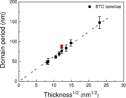
Substitution of this glassy layer thickness as that of an encapsulation layer () and using a domain wall energy density of =3×10⁻³Jm-1 Zhirnov1959 produced a remarkably good quantitative description of the observed domain periodicity data, as can be seen in figure 4. This strong agreement was obtained without any free fitting parameters, and one might naturally conclude that all of the encapsulation suffered by the BaTiO3 lamellae was indeed due to the constraint from the ion beam damaged layers.
(c)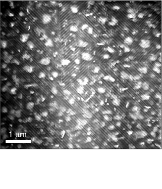
However, we have spent some considerable effort to develop processing methodologies to repair the surface damage caused by focused ion beam processing. Thermal annealing in air at 700 ℃ has been seen to both recrystallise the damage and expel the implanted gallium (forming thin gallium oxide platelets), recovering pristine single crystal BaTiO3 Saad2004 ; Schilling2007c ; Chang2008 (see figure 5). If the thermal annealing is performed in oxygen, then functional measurements even suggest that the permittivity of the surface region is the same as that seen in bulk Saad2004 ; Chang2008 .
The domain structure seen in a lamella which had been thermally annealed and is expected to have no surface damage is shown in figure 5-c. The domain appearance is almost identical to the unannealed sample in Figure 1, with the domain walls still of 110-type, indicating that 90°domain sets have again formed. While gallium oxide platelets have precipitated on the annealed surface (the white blotches in figure 5-c), these platelets certainly do not form a continuous layer, and it seems unlikely that they can provide the homogeneous stress needed to induce the 90°domain sets observed. Further, when the periodicity of the domains is analysed and compared to that obtained in unannealed lamellae, only a slight increase in domain period is observed; the increase in domain period is in fact consistent with an effective increase in the thickness of the lamella by 40nm (that associated with the recrystallisation of the amorphous glassy regions described above). The essential physics at play therefore appears to be unchanged even when the extrinsic damage layer is removed.
Overall, then, it appears that the quantitative agreement between the model and our data may be fortuitous, and that the stress responsible for the domains is not necessarily coming from the glassy barium titanate. Instead, a more fundamental source of stress must be at play for all of the FIBed single crystal barium titanate lamellae investigated to date. This suggests the existence of an intrinsic surface relaxation layer, probably due to surface tension.
The existence of surface layers in BaTiO3 has been known for quite some time Takeuchi1994 ; Tanaka1998 ; Anliker1954 ; Kanzig1955 ; Tsai1994 ; Vanderbilt1997 ; Vanderbilt1999 ; Rabe2005 ; Vanderbilt2007 ; Rappe2008 , yet there is surprisingly little agreement about their properties. Experimentally, their thickness seems to be on the region of 5-10 nm or more Takeuchi1994 ; Tanaka1998 ; Anliker1954 ; Kanzig1955 ; Tsai1994 , whereas first principles calculations give a much smaller value, about 1nm Vanderbilt1997 ; Vanderbilt1999 ; Rabe2005 ; Vanderbilt2007 . In some works the SL is found to be tetragonal at all temperatures, even above Tc Anliker1954 ; Kanzig1955 , where in others it is cubic even below Tc Takeuchi1994 ; Tanaka1998 . In fact, the structure of the SL can be rather complex and depends on processing conditions Rappe2008 . Nevertheless, what is important from the point of view of our model is not so much the exact symmetry of the surface , but the fact that it does not undergo the same ferroelectric/ferroelastic phase transition as the inside of the film. Thus, when the film becomes ferroelectric, it automatically becomes stressed by the untransformed surface layer. The present model requires only the induced stress is isotropic or orthotropic, and this is the case not only with cubic SL’s, but also with either amorphous SL or with tetragonal SL provided that the tetragonal axis is out-of-plane.
On the other hand, the elastic energy stored by the surface layer is proportional to its thickness. The outstanding question, then, is whether an intrinsic and very thin SL due to surface tension can lead to the same domain size as would be expected from the thicker encapsulation layers seen in our unnanealed samples.
Indeed, Eq.16 states that the domain size is essentially , independent of the SL thickness; however, this is equation is only valid when , which is not true if . On the other hand, our model has implicitly assumed that the stiffness (the shear modulus ) is the same for FL and SL, and this is unlikely when the SL is an intrinsic surface-tension layer; for these, the bonds are known to be shorter Vanderbilt2007 and the SL should be expected to be harder than the FL. It is relatively straight-forward to incorporate the different shear modulus of the surface layer () and the ferroelectric layer () onto the model, by simply substituting for and in eqs. (8) and (10) respectively. Minimization of the total energy then leads to the new generalized expression for domain size:
| (20) |
This expression is almost identical to (16) except for the appearance of the factor in the denominator. This factor can compensate for a reduced thickness of the surface layer insofar as its hardness is greater than that of the ferroelectric layer. Presently we have no quantitative estimates for the hardness of the intrinsic epilayer, and we very much encourage the theoretical community to perform first principles calculations of the value of . What we can say is that, if the thickness of the SL is only 1-2nm, as suggested by the ab-initio calculations Vanderbilt1997 ; Vanderbilt1999 ; Rabe2005 ; Vanderbilt2007 , its shear modulus would need to be roughly 10 times bigger than that of the FL to have the same effect on domain size as our 20nm extrinsic encapsulation layer. If, however, the true thickness of the intrinsic SL is ca. 10nm, as suggested by experimental measurements Takeuchi1994 ; Tanaka1998 ; Anliker1954 ; Kanzig1955 ; Tsai1994 then the SL need not be more any more rigid than the FL.
Conclusions
In sum, we have shown that, even in the absence of rigid substrates or any other source of external stress, ferroelastic twinning can appear due to the self-stress imposed by surface layers. The importance of such layers obviously increases as the size of the system decreases such that this effect becomes particularly important at the nanoscale. Furhermore, there need not be an extrinsic surface layer for the ferroelastic domains to appear; surface tension, which is intrinsic and therefore unavoidable, can also provide the necessary stress for domain formation. Finally, we note that epilayers can be expected to be important not only for isolated nano-ferroelectrics, but also in macroscopic devices such as ceramic capacitors made with nano-powders or core-shell grains.
This work was supported by the EC project FP6-STREP-MULTICERAL and by the French-UK collaboration program “Alliance”.
References
- (1) L. Landau and E. Lifshitz, Phys. Z. Sowjetunion 8, 153 (1935).
- (2) C. Kittel, Phys. Rev. 70, 965 (1946).
- (3) T. Mitsui and J. Furuichi, Phys. Rev. 90, 193 (1953)
- (4) S. K. Streiffer, J. A. Eastman, D. D. Fong, Carol Thompson, A. Munkholm, M.V. Ramana Murty, O. Auciello, G. R. Bai, and G. B. Stephenson, Phys. Rev. Lett. 89, 67601 (2002).
- (5) A. L. Roytburd, Phys. Status Solidi A 37, 329 (1976).
- (6) J. F. Scott, J. Phys. Cond. Mat. 18, R361 (2006).
- (7) A. Schilling, T. B. Adams, R.M. Bowman, J. M. Gregg, G. Catalan, and J. F. Scott, Phys. Rev. B 74, 024115 (2006).
- (8) G. Catalan, J. F. Scott, A. Schilling, and J. M. Gregg, J. Phys. Cond. Mat. 19, 022201 (2007).
- (9) V. A. Stephanovich, I. A. Luk’yanchuk, and M. G. Karkut, Phys. Rev. Lett., 94 047601 (2005).
- (10) F. De Guerville, I. Luk’yanchuk, L. Lahoche and M. ElMarssi, Mater. Sci. Eng. B 120, 16 (2005).
- (11) A. Schilling, R. M. Bowman, J. M. Gregg , G. Catalan, J. F. Scott, Appl. Phys. Lett. 89, 212902 (2006).
- (12) G. Catalan, A. Schilling, J. F. Scott and J. M. Gregg, J. Phys. Cond. Mat. 19, 132201 (2007).
- (13) A. Schilling, R. M. Bowman, G. Catalan, J. F. Scott, and J. M. Gregg Nano Lett. 7, 3787 (2007).
- (14) G. Catalan, H. Bea, S. Fusil, M. Bibes, P. Paruch, A. Barthelemy, and J. F. Scott, Phys. Rev. Lett. 100, 027602 (2008).
- (15) M. Daraktchiev, G. Catalan, J. F. Scott, Ferroelectrics 375, 122-131 (2008).
- (16) T. Takeuchi, K. Ado, T. Asai, H. Kageyama, Y. Saito, C. Masquelier, O. Nakamura, J. Am. Ceram. Soc. 77, 1665 (1994).
- (17) M. Tanaka and Y. Makino, Ferroelec. Lett. 24, 13 (1998).
- (18) J. Slutsker, A. Artemev, and Alexander Roytburd, Phys. Rev. Lett. 100, 087602 (2008).
- (19) W. Pompe, X. Gong, Z. Suo, and J. S. Speck, Appl. Phys. 74, 6012 (1993)
- (20) J. S. Speck and W. Pompe, J. Appl. Phys. 76, 466 (1994).
- (21) J. S. Speck, A. C. Datkin, A. Siefert, A. E. Romanov and W. Pompe, J. Appl. Phys. 78, 1696 (1995).
- (22) N. A. Pertsev and A. G. Zembilgotov, J. Appl. Phys. 78, 6170 (1995).
- (23) B. L. Cheng, M. Gabbay, and Fantozzi G, J. Mat. Sci. 31, 4141 (1996).
- (24) G. Bradfield, Nuovo Cim. 7, 182 (1950).
- (25) W. Ma, L.E. Cross, Flexoelectricity of BaTiO3, Appl. Phys. Lett. 88, 232902 (2006).
- (26) G. Catalan, L. J. Sinnamon, J. M. Gregg, J. Phys.: Condens. Matter 16, 2253 (2004).
- (27) G. Catalan, B. Noheda, J. McAneney, L. J. Sinnamon, and J. M. Gregg, Phys. Rev. B 72, 020102 (R) (2005).
- (28) M. S. Majdoub, R. Maranganti, P. Sharma, arXiv:0812.2083 (2008).
- (29) A. Zhirnov, Sov. Phys. JETP 35, 822 (1959).
- (30) B. Meyer and D. Vanderbilt, Phys. Rev. B 65, 104111 (2002).
- (31) N. Floquet and C. Valot, Ferroelectrics 234, 107 (1999).
- (32) D. Shilo, G. Ravichandran and K. Bhattacharya, Nat. Mater. 3, 453 (2004).
- (33) M. M. Saad, R. M. Bowman, and J. M. Gregg, Appl. Phys. Lett. 84, 1159 (2004).
- (34) A. Schilling, T. Adams, R. M. Bowman, J. M. Gregg, Nanotechnology 18, 035301(2007)
- (35) L. W. Chang, M. McMillen, F. D. Morrison, J. F. Scott, and J. M. Gregg Appl. Phys. Lett. 93, 132904 (2008).
- (36) M. Anliker, H. R. Brugger, and W. Kanzig, Helv. Phys. Acta 27, 99 (1954).
- (37) W. Kanzig, Phys. Rev. 98, 549 (1955).
- (38) Feng Tsai and J. M. Cowley, Applied Physics Letters 65, 1906 (1994).
- (39) J. Padilla and D. Vanderbilt, Phys. Rev. B 56, 1625 (1997).
- (40) B. Meyer, J. Padilla, and D. Vanderbilt, Faraday Discuss. 114, 395 (1999).
- (41) C. Bungaro and K. M. Rabe, Phys. Rev. B 71, 035420 (2005).
- (42) R. I. Eglitis and D. Vanderbilt, Phys. Rev. B 76, 155439 (2007).
- (43) A. M. Kolpak, D. Li, R. Shao, A. M. Rappe, and D. A. Bonnell, Phys.Rev.Lett. 101, 036102 (2008).