Tuning decoherence with a voltage probe
Abstract
We present an experiment where we tune the decoherence in a quantum interferometer using one of the simplest object available in the physic of quantum conductors : an ohmic contact. For that purpose, we designed an electronic Mach-Zehnder interferometer which has one of its two arms connected to an ohmic contact through a quantum point contact. At low temperature, we observe quantum interference patterns with a visibility up to 57%. Increasing the connection between one arm of the interferometer to the floating ohmic contact, the voltage probe, reduces quantum interferences as it probes the electron trajectory. This unique experimental realization of a voltage probe works as a trivial which-path detector whose efficiency can be simply tuned by a gate voltage.
pacs:
85.35.Ds, 73.43.FjProgress in nanofabrication techniques offers new opportunities to study quantum effects in small size conductors. A remarkable example has been the recent realization of electronic devices that mimic the optical Mach-Zehnder interferometer. The properties of these conductors have been successfully described using a ”simple” quantum scattering approach which considers electrons emitted by ”reservoirs” and scattered through the conductor. A limitation of this so-called Landauer-Büttiker theory is that it only treats elastic scattering. Therefore, it cannot account for decoherence or energy relaxation in electronic transport, a major issue for real devices. This limitation has been cunningly circumvented by theoreticians: they have introduced additional reservoirs whose connection to the studied quantum circuit mimics the decoherenceButtiker88IBMJRD32p63 . In these so-called voltage probes, electrons loose their quantum phase memory by thermalizing with the external world. Here we show the first quantitative realization of a voltage probe with a small ohmic contact which makes it possible to tune the decoherence in a quantum interferometer.
A reservoir in the physics of quantum conductors is defined as some region of the conductor which absorbs all incoming particles and emits ”new” particles with a Fermi statistics at the local electrochemical potential. Indeed, in the case of a sample larger than the electronic coherence length, one cannot tell exactly where are the reservoirs. They are simply assumed to be located at the multiple extremities of the conductor under consideration which exhibits quantum properties on a size scale determined by the coherence length of excitations, or their energy redistribution length. A voltage probe is a reservoir whose precise position and coupling to the circuit determines the location and the amount of decoherence.
The effect of a voltage probe can be explained in the following manner: quasi-particles which have been probed by this additional reservoir when going through the quantum conductor, loose their phase so that nothing differentiates them from the electrons of the reservoir. This theoretical construction is intimately linked to which-path experiments, in the sense that when an electron is absorbed by the additional reservoir, the ambiguity on the particle’s trajectory is lifted, suppressing interference effects. Energy relaxation can also be described within the same framework when the electrons are re-injected by the voltage probe into the interferometer at thermal equilibrium. Indeed, in the case of the electronic Mach-Zehnder interferometer, this approach has been used to predict the current fluctuations in the presence of decoherence or energy relaxation Marquardt04PRL92n056805 ; Marquardt04PRB70n125305 .
We present here an experiment where a voltage probe introduces a controlled energy redistribution. To this end, we have realized an electronic Mach-Zehnder interferometer (MZI) operating in the Quantum Hall Regime Ji03Nature422p415 . Here, the transport occurs through one dimensional chiral channels located at the edge of the sample (the edge states). These channels perfectly mimic the photon beam and hence one can realize an electronic counterpart to the optical interferometers. The voltage probe is obtained with a small floating ohmic contact connected to one of the arms of the interferometer through a controlled tunnelling barrier (a quantum point contact (QPC)). Floating ohmic contacts have already been used to enforce energy relaxation of noisy currents Sprinzak00PRL84p5820 ; Oberholzer06PRL96n046804 but without presenting an experimental set-up permitting the exploration of their dephasing properties. More specifically, the QPC allows us to tune the transmission probability towards the voltage probe. As a result, the visibility of the quantum interferences is reduced by a factor , which represents the probability amplitude for a particle not to be probed by the small floating ohmic contact.

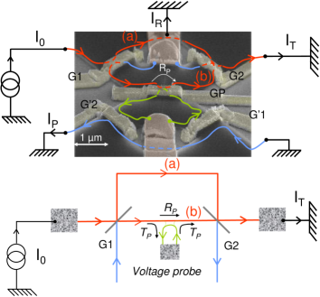
A SEM view of our MZI is represented in figure (1). Starting from a high mobility two dimensional electron gas in a GaAs/GaAlAs heterostructure with a sheet density of cm-2 and a mobility of cm2/Vs, we patterned the geometry of the mesa, thus the trajectory of the edge states, by e-beam lithography. The lengths of arms (a) and (b) were both designed to be equal to 5.7 m yielding an enclosed area of 7.25 m2. In our MZI (see figure (1)), there are 5 QPCs, G1, G2, G’1,G’2 and GP. G1 and G2 are the two beam splitters of the MZI itself, with transmissions tuned to 1/2 to obtain a maximum visibility of the interferences Roulleau07PRB76n161309 . GP, which is close to the trajectory (b), has two purposes. In the pinch-off regime, it is used to change the length of (b) in order to reveal the interference pattern. In addition, GP serves as a connection between (b) and the bottom small ohmic contact. We work at a filling factor 2 at a magnetic field of 4.6 T giving rise to two edge states. The inner one, not represented on figure 1, is fully reflected by G1 and G2.
We proceed as follows: we first fully open G’1 and G’2 to measure the transmission trough GP () as a function of its voltage . Once this reference obtained, we permanently close G’1 and G’2. The transmission probability through the MZI is measured by a standard lock-in technique with an AC excitation = 1.2 V smaller than , ensuring that the coherence length of the source is only limited by the experimental temperature of the order of 20 mK.
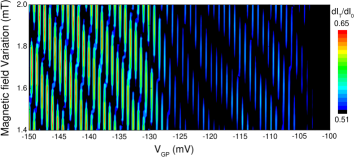
The interference pattern is revealed by varying either the magnetic field or . Hence, GP both connects the trajectory (b) to the voltage probe and sweep the phase difference between the two arms of the MZI. In figure 2, a color plot of the differential transmission versus the magnetic field and is displayed. As one can notice, the amplitude of the oscillations decreases as increases, i.e. when the trajectories are more connected to the voltage probe.

This visibility decrease is straightforward to understand. We call and the transmissions through the beam splitters G1 and G2 and the transmission to the voltage probe. The electron source injects an input current which has a probability to exit the MZI through the ohmic contact located on the right side of figure 1. As we treat a quantum circuit, is not the sum of the transmission probability of the different trajectories (path (a)+path(b)), but the squared sum of the transmission probability amplitudes. The transmission amplitude through the MZI is then the sum of three complex amplitudes corresponding to path (a), path (b) and those multiple reflected paths (labelled by j) which go through the small floating ohmic contact:
| (1) |
being random phases accumulated in the voltage probe, and and respectively stand for the reflection and transmission coefficient of electronic wavefunctions by QPC . This leads to a transmission probability , where , and . The first two terms of this expression correspond to the classical term whereas the third one, which reveals the wave nature of electrons, oscillates with the phase difference between the two arms. In the Quantum Hall Regime, this is equal to the Aharonov-Bohm phase corresponding to the magnetic flux threaded through the area delimited by the two interfering trajectories. It can thus be varied either by changing the enclosed area using GP or by sweeping the magnetic flux Roulleau07PRB76n161309 . The visibility of interferences defined as is:
| (2) |
where and are the maximum and minimum transmission respectively, is the measured visibility obtained when . As expected, this means that only the part of the wave function which does not go through the probe contributes to the interferences. Equation 2 is thus a consequence of the floating contact not affecting the mean current: all the charges that have been absorbed into it are re-injected into the circuit, so that the sum of the measured transmitted current and of the current absorbed by the upper small ohmic contact is conserved.

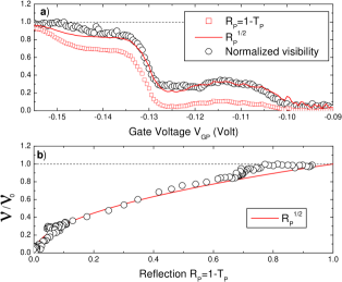
In previous which path experiments using quantum conductors, the dephasing occurred by coupling the electrons to a noisy electromagnetic environment Sprinzak00PRL84p5820 ; Buks98Nature391p871 ; Neder07PRL98p036803 ; Rohrlich07PRL98n096803 . In our set-up, electrons re-emitted into the interferometer cannot be distinguished from the other electrons of the probe. Reflecting their interactions with the various degrees of freedom of the floating contact, they bear a phase uncorrelated to the one of the incident electrons. Hence, they do not contribute to the quantum interferences that give rise to the Aharonov-Bohm term of the transmitted current. To perform a quantitative analysis of the voltage probe detection, we determined the transmission as a function of . This is achieved by measuring with and . The result is shown in figure (3a). Then we closed G’1 and G’2 such that . The normalized visibility as a function of is plotted in figure (3b). This is our main result, which shows the visibility increasing as the square root of the reflection probability, in perfect agreement with theory (Eq. (2)). It is noteworthy that despite the small size of the ohmic contact (less than m2), it shows no sign of Coulomb Blockade that would prevent electrons from entering it and protect quantum interferences. This is because the probe is connected through a metallic air bridge to a much bigger bonding pad. This strongly increases its capacitance and reduces its charging energy to a negligible level.
One can observe in figure (3a) that does not follow a monotonous Fermi function like variation as predicted by the saddle point model Buttiker90PRB41p7906 . There are two resonances near V and V, the first one () being associated with a discrepancy between the observed visibility and the law (see figure 3b). This is not the case for the second one. A resonance whose trajectory is included in the MZI should in principle be accompanied with a phase shift. As we will see, the second resonance has such a phase shift but not the first one. It means that around V, the measured conductance is not directly related to when and are almost closed.
Indeed, the phase variation of the interferences relates to the magnetic field variation and by , where is the quantum of flux . This phase variation leads to tilted black regions in figure 2, given by . At the resonance which appears in the measurement of for V, the separation between the tilted region is no longer regular, indicating that when crossing the resonance a additional phase shift appears in the interferences Avinun05Nature436p529 . Inspecting in detail the conductance trace for a given magnetic field as a function of we found a phase shift of approximately around this resonance, although our phase measurement is not precise enough to determine the exact shape of the phase variation. The absence of such phase shift in the other resonance close to V explains the small discrepancy with the law observed: when measuring , all the closed trajectories at a distance closer than the coherence length from GP Roulleau08PRL100n126802 ; Roulleau08PRL101n186803 could possibly lead to resonances. Here, we are in the case where the closed trajectory leading to this resonance is outside the MZI when G’1 and G’2 are at pinch off. Hence the value of the measured is not what should be taken into account for the visibility decrease.
To summarize, we have shown that a small floating ohmic contact is a voltage probe that can be used to destroy quantum interferences in a controlled way. For that purpose, we have used a QPC to drive the amplitude probability of the absorbtion of an electron in the voltage probe. Then, via interference measurements, we have proved that electrons absorbed and re-emitted by the probe acquire a random phase and do not contribute to the interference process. This work opens new possibilities regarding the study of the voltage and dephasing probe, the most promising being its full counting statistics, as recently proposed Pilgram06PRL97n066801 ; Forster07PRB75n035340 ; Forster07NJP9p117 .
References
- (1) M. Büttiker, IBM J. Res. Develop. 32, 63 (1988).
- (2) F. Marquardt and C. Bruder, Phys. Rev. Lett. 92, 056805 (2004).
- (3) F. Marquardt and C. Bruder, Phys. Rev. B 70, 125305 (2004).
- (4) Y. Ji et al., Nature 422, 415 (2003).
- (5) D. Sprinzak, E. Buks, M. Heiblum, and H. Shtrikman, Phys. Rev. Lett. 84, 5820 (2000).
- (6) S. Oberholzer et al., Phys. Rev. Lett. 96, 046804 (2006).
- (7) P. Roulleau et al., Phys. Rev. B 76, 161309(R) (2007).
- (8) E. Buks et al., Nature 98, 871 (1998).
- (9) I. Neder et al., Phys. Rev. Lett. 98, 036803 (2007).
- (10) D. Rohrlich et al., Phys. Rev. Lett. 98, 096803 (2007).
- (11) M. Büttiker, Phys. Rev. B 41, 7906 (1990).
- (12) M. Avinun-Kalish et al., Nature 436, 529 (2005).
- (13) P. Roulleau et al., Phys. Rev. Lett. 100, 126802 (2008).
- (14) P. Roulleau et al., Phys. Rev. Lett. 101, 186803 (2008).
- (15) S. Pilgram, P. Samuelsson, H. Förster, and M. Büttiker, Phys. Rev. Lett. 97, 066801 (2006).
- (16) H. Förster, P. Samuelsson, S. Pilgram, and M. Büttiker, Phys. Rev. B 75, 035340 (2007).
- (17) H. Förster, P. Samuelsson, and M. Büttiker, New Journal of Phys. 9, 117 (2007).