Broadband sensitive pump-probe setup for ultrafast optical switching of photonic nanostructures and semiconductors
Abstract
We describe an ultrafast time resolved pump-probe spectroscopy setup aimed at studying the switching of nanophotonic structures. Both fs pump and probe pulses can be independently tuned over broad frequency range between 3850 and 21050 cm-1. A broad pump scan range allows a large optical penetration depth, while a broad probe scan range is crucial to study strongly photonic crystals. A new data acquisition method allows for sensitive pump-probe measurements, and corrects for fluctuations in probe intensity and pump stray light. We observe a tenfold improvement of the precision of the setup compared to laser fluctuations, allowing a measurement accuracy of better than R= 0.07 in a 1 s measurement time. Demonstrations of the improved technique are presented for a bulk Si wafer, a 3D Si inverse opal photonic bandgap crystal, and z-scan measurements of the two-photon absorption coefficient of Si, GaAs, and the three-photon absorption coefficient of GaP in the infrared wavelength range.
pacs:
42.70.Qs, 42.65.Pc, 42.79.-eI Introduction
Optical pump-probe experiments Demtroder02 ; Siegman86 ; Diels96 are a powerful tool to study the ultrafast optical response of a wide range of effects in, for example, semiconductor physics,Muecke0 high harmonic generation,Esry06 and optics of biomembranes.Roke03 Recently, pump-probe techniques have also been extended to study ultrafast switching of photonic nanostructures such as photonic crystals Leonard02 ; Mazurenko03 ; Becker05 ; Euser07 and photonic cavities.Fushman07 ; Preble07 ; Harding07 In these studies, one literally attempts to catch light with light. Therefore such switching processes are susceptible to perturbing effects such as absorption or (induced) inhomogeneity,Euser05 and sensitive experimental methods are required.
In pump-probe experiments, high pump pulse intensities are often required to observe small changes in probe reflection or transmission. This requirement has led to the development of regenerative amplifiers, in which femtosecond (fs) pulses from Ti:Sapphire lasers are amplified to pulse energies of up to several mJ. The amplification process comes at a price of a strongly reduced repetition rate, typically from the MHz to the kHz range. The amplification step is often followed by conversion to different wavelengths using optical parametric amplifiers (OPA). Amplification processes typically increase pulse-to-pulse intensity variations of the laser.
There are two important issues that limit the speed and accuracy of pump-probe experiments. First, since experiments intrinsically depend in the magnitude of the irradiance, they are sensitive to pulse-to-pulse variations of the laser. The result is that long integration times are required to sufficiently reduce the fluctuation-induced error in probe reflectivity measurement. Secondly, scattered light from the intense pump pulses contributes to the background signal of the probe detector. In particular for strongly photonic samples, light is necessarily strongly scattered, therefore the background level can be larger than the reflectivity changes of the samples under study. To circumvent both potential issues, we have developed a versatile measurement scheme that allows for compensation for pulse-to-pulse variations in the output of our laser, as well as a subtraction of the pump background from the probe signal. Our technique strongly reduces the acquisition times required in pump-probe experiments, allowing for much more detailed scans than previously possible. While this paper focuses on the application to switching of semiconductors and nanophotonic structures through optical excitation of free carries, our results are relevant to any pump-probe experiment with regeneratively amplified laser pulses.
II pump-probe setup
II.1 Optical setup
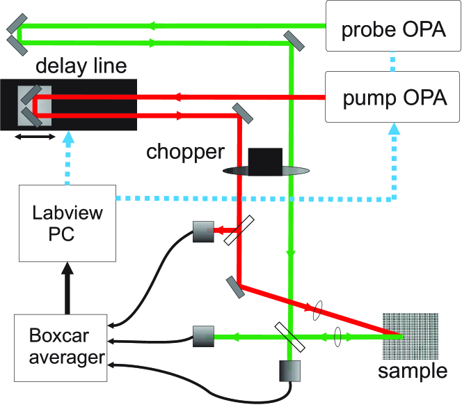
Time-resolved optical measurements on photonic crystals were performed with a dedicated two-color pump-probe setup. Our laser system provides high power pulses at two independently tunable frequencies, allowing us to adjust the pump frequency to optimize the optical penetration depthEuser05 and the probe frequency to scan across broad photonic gaps. The setup is based on a regeneratively amplified Titanium Sapphire laser that emits short 120 fs pulses at = 800 nm with a pulse energy of 1 mJ at a repetition rate of 1 kHz (Spectra Physics Hurricane). This laser drives two optical parametric amplifiers (OPA, Topas 800-fs) shown schematically in Fig. 1, that serve as pump and probe. The output frequencies of the OPAs are computer controlled, and can be continuously tuned between 3850 and 21050 cm-1. The excitation of carriers at pump frequencies near the two-photon absorption edge of semiconductors requires a high pump irradiance in the range of 10 to 300 GWcm-2, depending on the material and the pump frequency chosen.Euser05 Since both OPAs have a conversion efficiency that exceeds 30, a pulse energy of at least 20 J is available over the entire frequency range. The output of our OPAs consists of pulses with Gaussian pulse duration = 14010 fs (measured at = 1300 nm). The spectral shape of the output spectrum was measured to be Gaussian with a frequency independent linewidth = 1.440.05. We deduce the time-bandwidth product to be = 0.470.05, in good agreement with the Fourier limit for Gaussian pulses (= 0.44).Siegman86 To a good approximation, the temporal profile of the pulses has a Gaussian intensity envelope:
| (1) |
where is the peak power. Experimentally, we obtain the inside the sample by subtracting the pump reflectivity at the sample interface:
| (2) |
where is the external pump power, and R is the measured reflectivity of the pump beam at the sample interface at . Both pump and probe beams were focused onto the sample at a small numerical aperture NA= 0.02. The pump intensity profile was confirmed to be Gaussian with a radius = 1135 m. We can therefore describe the spatial irradiance distribution in the focus as Gaussian:
| (3) |
where is the peak irradiance in the center of the focus. Even with a large pump focus of = 1135 m, the maximum peak irradiance that can be obtained in our setup still exceeds 1 TWcm-2. This large excess irradiance indicates that it is feasible to switch an even larger sample, or to use less powerful lasers on small samples, which is important to facilitate possible future applications of ultrafast switching.
The probe beam was focused to a Gaussian spot of typical radius = 205, depending on the diffraction limited size of the spot given by . Since the probe focus is much smaller than the pump focus, we obtain excellent lateral homogeneity of the nonlinear excitation throughout the probe focus. This turns out to be crucial to permit successful physical interpretation of complex photonic structures. In all experiments, we explicitly ensured that only the central flat part of the pump focus is probed by testing with a Si wafer.
In Figure 1, the delay between pump- and probe pulse was set by a 40 cm long optical delay line with a time resolution of t= 10 fs. Since the delay time is also computer controlled, we can scan the reflectivity spectrum as a function of frequency at a chosen time delay after the pump pulse.
II.2 Data acquisition method
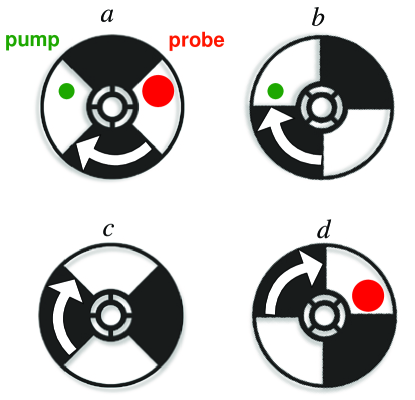
In our setup, the OPAs show typical relative irradiance variation between 2 RMS variation near = 1300 nm and of 7 in the worst case near the degeneracy point near = 1600 nm. If the signals are not corrected for, such variations in pump irradiance in a one-photon process would fundamentally limit the relative accuracy of the probe signal. To improve the signal-to-noise to better than the laser stability, it is important to probe individual pulse events so that pulse selection can be performed. Therefore, the irradiance of each pump and probe pulse is monitored by two InGaAs photodiodes and the reflectivity signal is measured by a third InGaAs photodiode, shown as black squares in Fig. 1. Three boxcar averagers are used to hold the short output pulses of each detector for 1 ms, allowing simultaneous acquisition of separate pulse events of all three detector channels by a data acquisition card. Both pump and probe beam pass through a chopper whose frequency is synchronized to the repetition rate of the laser ( = 1 kHz). The alignment of the two beams on the chopper blade is such that each millisecond, pump and probe beam are blocked or unblocked in a different permutation, shown in Fig. 2. In this flexible measurement scheme, detector signals for each pulse event are collected, allowing various data processing routines such as automatic background subtraction and the selection of pulses within a certain pump energy range after the experiment.
For a measurement on a reflecting sample, the linear (unpumped) reflectance is given by , where is the detector signal when the chopper is in position (d), while is the probe background signal measured at chopper position (c). To compensate for probe pulse fluctuations, is then ratioed by the background-corrected probe monitor signals , measured when the chopper is at position (d) and (c). As the background measurements are taken in between the reflectivity measurements, temporal fluctuations in the background signal originating from pump and from the surroundings are eliminated. In a similar manner, the non-linear (pumped) reflectance is equal to , where and are the signals measured on R at chopper positions (a) and (b), respectively. This signal is also ratioed to the corresponding probe monitor signals. This process obviously requires the three detectors to store all four signals during a time (). When this happens, the differential reflectivity corrected for background and fluctuations is thus determined by
| (4) |
The signal is offered to the DAC card by the boxcar measuring the sample reflectance. Neglecting electronic amplification factors, is equal to the magnitude of the time- and space integrated Poynting vector ,
| (5) | |||||
Here, the beam is collimated to a radius and is the integration time of the boxcar. and denote the permittivity and permeability of free space, respectively. The electric field reflected by a sample onto the detector can be separated in a Gaussian envelope of temporal width (see Eq. 1) and amplitude , multiplied by a sinusoidal component with a carrier frequency in rad/s.111This Slowly Varying Envelope Approximation (SVEA, see, e.g. Ref. Diels96, ) can be applied to pulses where , and where does not change over , i.e., for bandwidth limited pulses. The squared oscillating term can then be integrated separately and yields , and the time integration can be taken to infinity because . Since the integration time of the boxcar ( 150 ns) is much longer than any probe pulse duration, the dynamics of the sample is essentially integrated over.
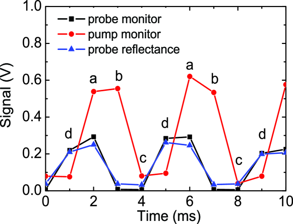
Figure 3 shows a typical time trace for probe monitor, pump monitor and reflected probe signal collected by the data acquisition card. Note that between 1 ms (pump off) and 2 ms (pump on) the probe reflectance signal goes up, suggesting an increase in reflectivity, while between 5 and 6 ms, the probe reflectance signal decreases. These artifacts are caused by the pulse-to-pulse variations in the laser output, and are easily eliminated in our method by referencing to the probe monitor signal. An additional advantage of our scheme is that excited and linear reflectivity signals can be simultaneously monitored on an oscilloscope, which greatly facilitates the alignment procedure.
III Experimental results
In this section we will demonstrate how our technique yields precise nonlinear reflection and transmission measurements, both on intricate photonic crystal samples as well as on bulk semiconductors.
III.1 Statistical analysis of measured data
In this section we describe the statistical analysis of the data collected in our experiments. At each time delay and for each wavelength setting for the probe OPA, all detector signals from 4x250 pulse events were collected and stored. The probe reflectance signal for 4x250 pulse events of a pump-probe experiment on a GaAs/AlAs multilayer structure is plotted versus probe monitor signal in Figure 4. Experimental details for this structure can be found in Ref. Euser07b, . Both signals show a variation as a result of the pulse-to-pulse variations of the laser. The datapoints constitute two separate lines whose slopes correspond to the unpumped and pumped reflectance of the sample. To exemplify the noise reduction of our method, we have chosen a data set during which the alignment of the pump laser was not optimized and pulse-to-pulse variations of the probe signal were larger than normal, amounting to a large relative standard deviation = 13.
The corresponding standard error in the mean detector signal is R/R=/= 13/= 0.8, which is relatively large compared to the effects that we wish to study. We therefore use an automated data processing routine to process the probe reflectance and probe monitor data to increase the signal-to-noise ratio. From the entire data set, the averages of the background levels (b) and (c) were determined, and subtracted from the pumped (a) and unpumped (d) reflectance data respectively (see Fig. 2). The resulting background-subtracted reflectance signal was divided by the corresponding monitor signal to compensate for intensity variations in the output of the laser. Through this procedure, the RMS variation in the unpumped reflectivity that was found from the data in Fig. 4 was strongly reduced to = 1.1. We attribute the remaining noise to uncorrelated electronic noise in the detection system. The resulting standard error in the probe reflectivity is thus tenfold improved to R/R= 0.07, even if the laser is not running optimally. Our scheme allows a sensitive measurement of the reflectivity and of small reflectivity changes, while maintaining an acceptable measurement time of about 1 second per frequency-delay setting.
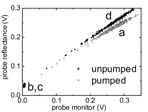
Pulse to pulse variations in the pump energy are a more subtle issue, since such fluctuations will often propagate in a nonlinear, and sometimes unpredictable, way in the reflectivity change R/R of the sample. The open circles in Fig. 4 correspond to the switched reflectance data. The slope of the line that is formed by these data points is reduced by about 10 compared to the unswitched data (closed squares). The corresponding reflectivity decrease is equal to R/R= 10. We also observe that the line is about twice as broad as the line corresponding to the unpumped data. We attribute the broadening to pulse to pulse variations of the pump beam.
In the example in Fig. 4 the standard deviation of the pump pulse energy = 12, from which we deduce a standard error in the pump irradiance = = 0.8. The error in the reflectivity change R/R due to the pulse-to-pulse irradiance fluctuations is equal to (R/R)= 2(R/R), where the factor 2 is due to the quadratic dependence of R/R on for a two-photon process. Using the reflectivity change in the data in Fig. 4 (R/R= 10) we obtain the pump contribution to the standard error in R/R to be (R/R)= 0.16. The error in reflectivity changes R/R also contains a contribution of the fluctuations in the probe pulse that were discussed before. The error due to the probe variation is equal to R/R)= 0.1, since the two independent errors in the pumped- and unpumped datasets are added. We calculate the total error by adding the contributions of both probe and pump variations. We obtain a standard error:
| (6) |
which is sufficiently sensitive for our switching experiments.
In some applications, an even higher sensitivity is required. Fortunately, pump-monitor detector signals for each individual pulse event are stored. It is thus possible to reduce the pump term in Eq. 6 by selecting pump pulses within a certain narrow energy range after the experiment, at the expense of longer integration times. Alternatively, in experiments where the relation between pump intensity and sample response is linear, the pump-monitor signal can be used to correct the measured signal. In our switching experiments on photonic nanostructures, however, such a correction cannot be made since the sample response is typically nonlinear with pump intensity. Therefore a pulse selection procedure was applied in z-scan measurements (see Section III.4), where pump stability is essential for the correct interpretation of the experimental data. Our strongly improved sensitivity has recently allowed us to identify two femtosecond contributions to the spectral properties of a switched Si woodpile photonic bandgap crystal: the optical Kerr effect, and nondegenerate two-photon absorption.Harding08
III.2 Ultrafast switching of bulk Si
An example of free carrier-induced change of refractive index in bulk silicon is given in Fig. 5 (upper panel). In this experiment, a powerful ultrashort pump pulse with wavelength = 800 nm was focused to a spot with radius wpump=7010 m, resulting in a peak irradiance at the sample interface of I0= 11540 GWcm-2. The reflectivity of a weaker probe pulse (= 1300 nm) with a smaller spot radius of wprobe= 205 m was measured in the center of the pumped spot at different time delays with respect to the pump pulse. The scan in Fig. 5 (upper panel) shows that the reflectivity of the sample changes from to . The rise time is 230 fs, clearly an ultrafast change in refractive index . From Fresnel’s formula we find the refractive index change to be more than . The lower panel shows the intensity autocorrelation function (ACF) of the pump pulses. The full width half maximum (FWHM) is 200 fs, we therefore conclude that the free carriers have been generated almost instantaneously.
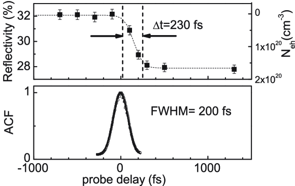
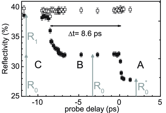
Fig. 6 shows reflectivity from an extended probe delay range of -12 to +5 ps. Quite remarkably, at a negative probe delay of 8.6 ps, we observe an additional large step in the reflectivity from 38 to 32. We can identify three distinct probe delay regimes A, B, and C, which are separated by two large steps in the reflectivity. The time difference between the first and second step is 8.60.5 ps, this value corresponds well to twice the optical thickness of the wafer = 8.30.1 ps, where = 3.5 is the refractive index of Si at = 1300 nm,Palik85 and = 3565 m is the measured thickness of the wafer.
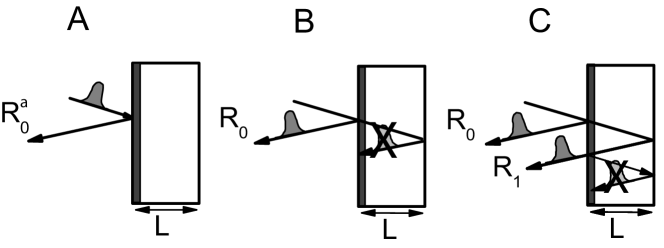
To interpret the observed unusual time dependence, we show in Fig. 7 snapshots of the reflected irradiance, taken at the moment that the pump pulse switches the front face of the wafer. The reflectivity of the wafer consists of multiply reflected pulses from front and back surface of the wafer, which are indicated by , , and . The magnitude of each successive reflection is given by . We neglect any reflections beyond in our analysis. It is important to note that each subsequent reflection is delayed with respect to by an even multiple (2m) of the optical thickness tm= 2m.
The pump conditions in the experiment in Fig. 6 result in an inhomogeneous, dense carrier plasma near the front face of the wafer.Euser05 Free-carrier absorption and diffraction from the dense plasma results in a strongly attenuated transmission. The plasma thus acts as an ultrafast shutter that blocks internally reflected pulses that arrive at the front face after the switching. At probe delay A, the pump arrives before reflection , and the measured signal corresponds to the reflection of the switched wafer, indicated by . At delay setting B, the pump pulse arrives in between reflection and , thus blocking and . This reflection corresponds to the front face refection of the unswitched wafer . In Fig. 6 we observe that the reflection in this time range is indeed comparable to the Fresnel reflection from a single air-Si interface (R= 31). At probe delay C, the pump pulse arrives in between reflection and , and only is blocked. The total reflection is thus equal to +. We note that the reflectivity changes in a switched double side polished wafer are very large, particularly when the back face reflection is blocked. Double side polished Si wafers are therefore ideal test samples to find- and optimize the spatial- and temporal overlap of our pump and probe pulses.
III.3 Ultrafast switching of 3D Si inverse opal photonic bandgap crystals
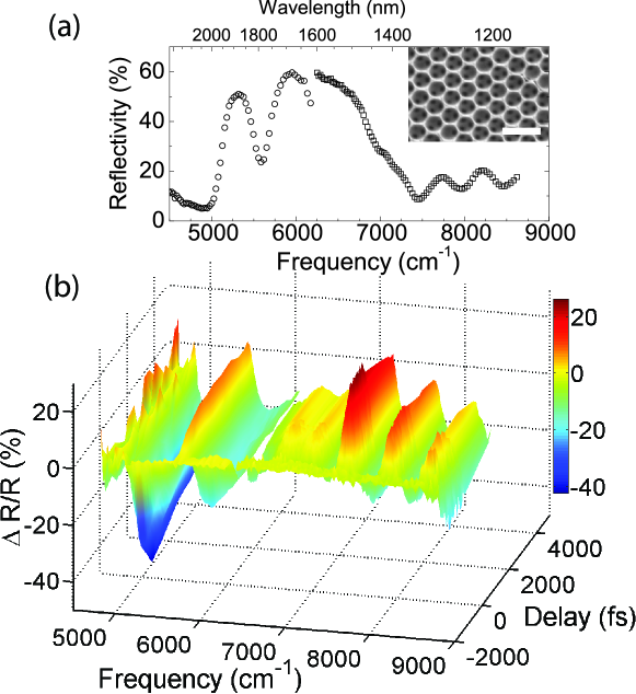
As a second example we demonstrate ultrafast switching experiments that were carried out on the Si inverse opal photonic crystal shown in Fig. 8(a) (inset). The broadband reflectivity data, shown in Fig. 8(a) covers the complete range of second order stop bands in our crystal where a 3D photonic band gap has been predicted.Vlasov01 A two-photon process was used to homogeneously excite carriers in the photonic crystal. The pump frequency was chosen in relation to the probe frequency range, to allow polarization based separation of pump and probe light. The time and frequency resolved differential reflectivity of the crystal R/R() at ultrafast time scales is represented as a three-dimensional surface plot in Fig. 8(b). The plot contains over 1500 datapoints, each obtained from 500 or 1000 single pulse measurements and represents nearly an octave on probe frequency. Such a large scanning range is typically required for strongly photonic crystals, since their photonic gaps have large bandwidths. The data collection was performed in as little as 40 minutes, much shorter than in conventional setups without automated scanning, -referencing and -background subtraction.Leonard02 ; Mazurenko03 ; Becker05 The data show clear dispersive shapes in the differential reflectivity, caused by a shift of the peaks towards higher frequency. We observe a large frequency shift of up to = 1.5 of all spectral features including the peak that corresponds to the photonic band gap. We deduce a corresponding large refractive index change of = 2.0, where is the refractive index of the silicon backbone of the crystal. Our broad probe scanning range allowed us to observe that both the low and high frequency edge of the stop bands have shifted. This indicates the absence of separate dielectric and air bands in the range of second order Bragg diffraction in inverse opals, which is consistent with predictions based on quasistatic band structure calculations. A detailed description of the ultrafast switching of Si inverse opal photonic bandgap crystals is presented in Ref. Euser07, .
III.4 Z-scan measurements on GaP at IR wavelengths.
As a final demonstration of our technique, we have obtained open aperture z-scan data for the semiconductors GaP, Si, and GaAs. A detailed description of these experiments is given in Appendix Appendix. In this section we present measurements of the three-photon absorption coefficient of GaP, a highly suitable material for photonic bandgap crystals because of its high refractive index and low absorption in the visible wavelength range. The pump wavelength was chosen in the range of three-photon absorption: . We therefore neglect both linear and two-photon absorption in our analysis (== 0). The resulting equation for the nonlinear transmission of the sample, normalized to the linear transmission is:
| (7) |
where is the three-photon absorption coefficient.
Fig. 9(a) shows typical z-scan data taken at a wavelength = 1600 nm, close to the three-photon absorption edge of GaP. We observe that the z-scan data in Fig. 9(a) is asymmetric; the transmission of the sample is slightly elevated at positive z-values, where the sample is located in between the beam waist and the detector. This asymmetry of less than 5 indicates that nonlinear refraction also plays a role in this experiment, and represents a slight deviation from a true open aperture z-scan. From the shape of the curve we conclude that the sign of the nonlinear refraction in GaP is positive in the wavelength range 1400-1600 nm. We therefore exclude that the asymmetry is caused by free-carriers generated by three-photon absorption, since this would result in a negative refractive index change.
To obtain the three-photon absorption coefficient for GaP, we disregard the relatively small nonlinear refraction. We compare our results to a numerically calculated transmission curve, shown in Fig. 9(a). We have varied until the depth of the minimum of the calculated scan matches the data. The calculated curve agrees well with the data. At = 1600 nm, we deduce = 1.00.310-3 cm3GW-2. Four additional scans were made at = 1400 nm, = 1450 nm, = 1500 nm, and at = 1550 nm. The resulting deduced three-photon absorption coefficients are plotted versus frequency in Fig. 9(b). We observe that tends to zero as the frequency approaches the , similar to what was observed in Ref. Pearl08, for Si. The frequency scaling confirms a three-photon absorption process. We propose that the observed opposite sign of the negative refractive index change by free-carrier effects and the positive change due to nonlinear refraction in GaP allows for intricate non-monotonic temporal switching of GaP photonic crystals.Tjerkstra08 This effect would allow ultrafast back-and-forth switching of photonic gaps.Harding08
(A). (B).
(B). 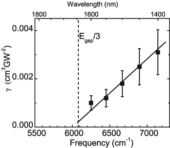
The results of the z-scan measurements that were performed on Si and GaAs in the frequency range close to half the electronic bandgap are summarized in Table 1. The Si data are in good agreement with Refs. Dinu03, ; Bristow07, . The GaAs data are in excellent agreement with Ref. Hurlbut07, . The experiments are described in detail in Appendix Appendix.
| Material | [nm] | [cmGW-1] |
|---|---|---|
| Si | 1630 | 0.6 0.3 |
| Si | 1720 | 0.20.1 |
| Si | 2000 | 0.20.05 |
| GaAs | 1630 | 3.51.0 |
| GaAs | 1720 | 1.50.5 |
IV Conclusions
We have built a two-color pump-probe setup that provides high energy, ultrashort laser pulses at optical frequencies in the range between 3850 and 21050 cm-1. Our versatile measurement scheme automatically subtracts the pump background from the probe signal and compensates for pulse-to-pulse variations in the output of our laser. We deduce a tenfold improvement of the precision of the setup, allowing a measurement accuracy of better than R= 0.07 in a 1 s measurement time, even if the laser is not running optimally. Demonstrations of the technique are presented for a bulk Si wafer, 3D Si inverse opal photonic bandgap crystal, GaAs/AlAs photonic structures, and z-scan measurements on bulk semiconductors.
ACKNOWLEDGMENTS
We thank Cock Harteveld, Frans Segerink, and Rindert Nauta for technical support, Soile Suomalainen and Mircea Guina for the Bragg stack sample, the group of David Norris for the Si inverse opal, and Mischa Bonn for useful remarks. This work is part of the research program of the ”Stichting voor Fundamenteel Onderzoek der Materie” (FOM), which is supported by the ”Nederlandse Organisatie voor Wetenschappelijk Onderzoek” (NWO). WLV thanks FOM for a ”Inrichting leerstoelpositie” grant, and support from NWO/VICI and STW/NanoNed.
References
- (1) ”Laser Spectroscopy: Basic Concepts and Instrumentation”, Ed. W. Demtröder (Springer-Verlag, Berlin, 3 edition, 2002).
- (2) ”Lasers”, A. E. Siegman (University Science Books, Mill Valley, USA, 1986).
- (3) ”Ultrashort laser pulse phenomena”, J- .C. Diels and W. Rudolph (Academic Press, USA, 1996).
- (4) O. D. Mücke, T. Tritschler, M. Wegener, U. Morgner, and F. X. Kärtner, Phys. Rev. Lett. 87, 057401 (2001).
- (5) B. D. Esry, A. M. Sayler, P. Q. Wang, K. D. Carnes, and I. Ben-Itzhak, Phys. Rev. Lett. 97, 013003 (2006).
- (6) S. Roke, J. Schins, M. Müller, and M. Bonn, Phys. Rev. Lett. 90, 128101 (2003).
- (7) S. W. Leonard, H. M. van Driel, J. Schilling, and R. B. Wehrspohn, Phys. Rev. B 66, 161102(R)(2002).
- (8) D. A. Mazurenko, R. Kerst, J. I. Dijkhuis, A. V. Akimov, V. G. Golubev, D. A. Kurdyukov, A. B. Pevtsov, and A. V. Sel kin, Phys. Rev. Lett. 91, 213903 (2003).
- (9) C. Becker, S. Linden, G. von Freymann, M. Wegener, N. Tétreault, E. Vekris, V. Kitaev, and G. A. Ozin, Appl. Phys. Lett. 87, 091111 (2005).
- (10) T. G. Euser, H. Wei, J. Kalkman, Y. Jun, A. Polman, D. J. Norris, and W. L. Vos, J. Appl. Phys. 102, 053111 (2007).
- (11) I. Fushman, E. Waks, D. Englund, N. Stoltz, P. Petroff, and J. Vuckovic, Appl. Phys. Lett. 90, 091118 (2007).
- (12) S. F. Preble, Q. Xu, and M. Lipson, Nat. Photonics 1, 293 (2007).
- (13) P. J. Harding, T. G. Euser, Y. Nowicki-Bringuier, J. M. Gérard, and W. L. Vos, Appl. Phys. Lett. 91, 111103 (2007).
- (14) T. G. Euser and W. L. Vos, J. Appl. Phys. 97, 043102 (2005).
- (15) T. G. Euser, H. Wei, J. Kalkman, Y. Jun, M. Guina, S. Suomalainen, A. Polman, D. J. Norris, and W. L. Vos, In ”Active Photonic Crystals”, Ed. S. M. Weiss, G. S. Subramania, F. Garcia-Santamaria, Proc. SPIE 6640, 66400G: 1-4 (2007)(Invited paper).
- (16) P. J. Harding, T. G. Euser, and W. L. Vos, J. Opt. Soc. Am. B (Accepted) http://arxiv.org/abs/0807.4459
- (17) ”Handbook of optical constants of solids”, E. D. Palik, (Academic press Inc., London 1985).
- (18) Y. A. Vlasov, X- Z. Bo, J. C. Sturm, and D. J. Norris, Nature 414, 289 (2001).
- (19) S. Pearl, N. Rotenberg, and H. M. van Driel, Appl. Phys. Lett. 93, 131102 (2008).
- (20) R. W. Tjerkstra, F. B. Segerink, J. J. Kelly, and W. L. Vos, J. Vac. Sci. Technol. B. 26, 973-977 (2008).
- (21) M. Dinu, F. Quochi, and H. Garcia, Appl. Phys. Lett. 82, 2954 (2003).
- (22) A. D. Bristow, N. Rotenberg, and H. M. van Driel, Appl. Phys. Lett. 90, 191104 (2007).
- (23) W. C. Hurlbut, Yun-Shik Lee, K. L. Vodopyanov, P. S. Kuo, and M. M. Fejer, Opt. Lett. 32, 668 (2007).
- (24) M. Sheik-Bahae, A. A. Said, and E. W. van Stryland, Opt. Lett. 14, 955 (1989).
- (25) M. Sheik-Bahae, D. J. Hagan, and E. W. Van Stryland, Phys. Rev. Lett. 65, 96 (1990).
- (26) M. Sheik-Bahae, A. A. Said, T. H. Wei, D. J. Hagan, and E. W. van Stryland, IEEE J. Quantum Electron. 26, 760 (1990).
- (27) M. Sheik-Bahae, A. A. Said, T. H. Wei, D. J. Hagan, and E. W. van Stryland, IEEE J. Quantum Electron. 27, 1296 (1991).
- (28) M. Balu, J. Hales, D. J. Hagan, and E. W. Van Stryland, Opt. Express 16, 3840 (2004).
Appendix
IV.1 Two-photon absorption in Si
An elegant method to measure the nonlinear refraction of semiconductors is the z-scan technique that was first demonstrated by Sheik-Bahae et al..Sheikbahae89 ; Sheikbahae90b A z-scan is a simple and robust measurement of the transmission of a single beam that is focused by a lens. The focal length of the lens is chosen such that the focal depth is much larger than the sample thickness. The transmitted power of a focused laser beam is measured while the sample is scanned in the z-direction, along the optical axes of the beam, see Fig. 10. The nonlinear refraction results in both Kerr-lensing due to the change in real part of the refractive index, as well as attenuation of the transmitted power due to nonlinear absorption. Both effects will attain a maximum if the sample is located in the beam waist (z=0).
To separate the refractive and absorptive effects, two scans must be made. The first experiment is a closed aperture z-scan, in which refraction and absorption are measured simultaneously. A diaphragm that is placed in front of the detector blocks part of the linearly transmitted light. For example, a positive will induce a positive Kerr lens in the sample, which will guide more light into the detectors if the sample is placed at a positive z-position in between the beam waist and detector (see Fig. 10). The transmitted intensity will be reduced if the sample is placed in between the lens band beam waist. The nonlinear refraction will cause an asymmetry in the z-scan data. The second experiment is a an open aperture z-scan, in which the aperture is removed, and all transmitted light is collected. The effect of nonlinear refraction is thus removed. The resulting curve only depends on the induced absorption, and is therefore symmetric around the beam waist (z=0). By subtracting the open aperture data from the closed aperture data, the refractive and absorptive effects can be separated.Sheikbahae90a ; Sheikbahae91 ; Dinu03 ; Balu04
In our switching experiments we are mostly interested in the nonlinear absorption coefficients near the two-photon absorption edge of Si and GaAs. Therefore this Appendix describes open aperture z-scan experiments that were done on Si and GaAs single crystalline wafers. To the best of our knowledge the results presented here are the first measurements of the two-photon absorption coefficient GaAs near the two photon absorption edge ().
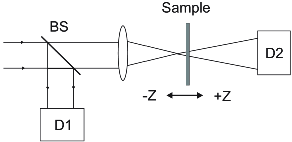
Fig. 10 shows a schematic drawing of our z-scan setup. The power of the incoming beam is monitored by detector D1. The beam is focused by a lens with focal length . The sample, typically a double-side polished wafer, is placed on a translation stage that scans the sample along the z-direction. The zero position is taken at the beam waist. The transmitted power is collected by a second lens (not shown) and measured by a InGaAs photodiode D2.
The shape of the transmission curve strongly depends on pump irradiance, and pump power stability is therefore essential for the correct interpretation of the experimental data. Each pulse was therefore measured individually using the detection scheme described in Section II.1. Both pump-monitor detector signals (D1) and transmission signals (D2) for each pulse event are stored. We minimize the effect of pulse-to-pulse variations in the laser output (which can be as high as 10) by selectively removing all pulses with energy beyond a certain threshold. In all experiments, the number of pulses collected and the threshold were chosen such that the standard deviation in pump energy remained below 3. Typically between 2500 and 10000 pulses were collected for each datapoint. The corresponding standard error in the transmission was typically better than T/T1, which is sufficiently sensitive for our z-scan measurements. The sensitivity can be further increased by narrowing the pulse energy range, at the price of longer integration times.
IV.2 Model
To interpret the z-scan data, we have numerically calculated the nonlinear transmission of a Gaussian beam through a thin slab. The beam radius of a diffraction limited Gaussian beam is
| (8) |
where is the wavelength, z is the sample position relative to the focus.Demtroder02 The diffraction limited radius of the beam waist is equal to:
| (9) |
where is the focal length of the lens and is the Gaussian radius of the unfocused beam at the position of the lens. At each wavelength, was determined by a knife edge scan.
In our calculation we have discretized the sample into 256256 independent transmission channels of 1010 m2. We have made sure that the lateral dimensions of each channel are smaller than the focus radius , to avoid discretization artifacts at z=0. We calculate the nonlinear transmission through each channel. Since our pump frequencies are in the two-photon absorption range where =0, therefore, the transmitted power through a sample with thickness L, normalized to the linear transmission is equal to:
| (10) |
where R is the Fresnel reflectance at the front- and back-face of the sample, is the two-photon absorption coefficient, and the irradiance at the sample interface after subtraction of the front-face reflection at position z. The added calculated transmission of all channels is plotted versus sample position z. The adjustable parameter in this calculation is .
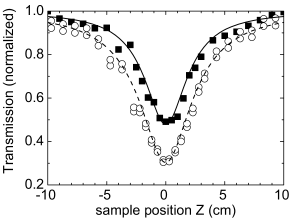
First we consider open aperture z-scan measurements on a double-side polished Si wafer with thickness L= 360 m. Normalized transmission is plotted in Fig. 11 as a function of sample position z. Data were taken at two wavelengths: = 1630 nm (open circles) and at = 1720 nm (closed squares). The measured data were normalized to the linear transmission away from the focus. We observe that in both scans, the transmission is strongly reduced as the sample scans through the focus. The curves are numerically calculated transmission data, where was used as fitting parameter. We find good agreement for = 0.60.3 cmGW-2 (= 1630 nm), and for = 0.20.1 cmGW-1 at = 1720 nm. Fig. 12 shows a z-scan of the same Si wafer at a pump wavelength = 2000 nm, close to the two-photon absorption edge of Si. The peak irradiance during this scan was = 800200 GWcm-2. We find good agreement for = 0.200.05 cmGW-1.

IV.3 Two-photon absorption in GaAs
We have performed open aperture z-scan experiments on a double-side polished GaAs wafer with a thickness of 189 m. Figure 13 shows z-scan data taken at = 1720 nm, just above the two-photon absorption edge of GaAs. The measured data were normalized to the linear transmission away from the focus. The peak irradiance was = 36660 GWcm-2 in Fig. 13. The strongly attenuated transmission near the waist of the beam indicates a strong nonlinear absorption. The curve is calculated using as an adjustable parameter. We find good agreement for = 1.50.5 cmGW-1. Fig. 14 shows z-scan data for GaAs at a shorter wavelength = 1630 nm. Here, we find good correspondance for = 3.51.0 cmGW-1. Our data are in excellent agreement with Ref. Hurlbut07, . We conclude that in GaAs, the two-photon absorption coefficient strongly decreases as the pump wavelength approaches half the band gap energy, allowing spatially more homogeneous switching.Euser05


We have measured the two-photon absorption coefficients of Si and GaAs near the two-photon absorption edge by an open-aperture z-scan technique. The experimental data was compared to a model that includes nonlinear absorption in the sample. For both Si and GaAs we find that the two-photon absorption coefficient tends to zero near half the gap energy .