=0.4cm
Transmission properties of optical adhesives and bonding layers
Abstract
We analyze the transparency of a thin film of low refractive index (an optical glue or a bonding layer) placed between higher-index media and forming an opto-pair. Examples include a semiconductor light-emitting diode with attached lens or a semiconductor scintillator bonded to a photodiode. The transparency of an opto-pair is highly sensitive to the film thickness due to the so-called frustrated total internal reflection. We show that high transparency in a wide range of the incidence angle can be achieved only with very thin layers, more than an order of magnitude thinner than the wavelength. The angular dependence of the transmission coefficient is shown to satisfy a simple and universal sum rule. Special attention is paid to the angular average of the optical power transmission, which can be cast in a universal form for two practically relevant classes of source layers.
Introduction
A number of semiconductor optoelectronic devices require optical matching of their component layers. Semiconductor light emitting diodes (LED) have low external emission efficiency limited to 2-4 % due to the high refractive index of the source crystal, resulting in a narrow escape angle of total internal reflection (TIR) Moss . To avoid the TIR, various techniques have been used including random surface texturing, pyramidal-shaped structures, as well as devices exploiting “wave optics” effects and optimizing interference in the resonant cavity (see Delbeke for the review). The most effective remedies for the TIR effects in LEDs are optically tight lenses, resulting in external emission efficiencies approaching unity LED1 ; LED2 . Another example when optical matching matters is a semiconductor scintillator used for the detection of high-energy particles with the scintillating radiation registered by a photodiode Serge . In both cases the optical components can be attached by using optical adhesives or optical glues in the form of a thin interlayer. The refractive index of the interlayer is considerably lower than that of both semiconductors. It is usually expected that films thinner than wavelength should not disturb the radiation transmission or waveguiding properties Bowers . This is indeed true for normal incidence. Moreover, for a fixed angle of incidence the transparency can be generally enhanced by choosing the thickness of the low-index layer so as to provide constructive interference for the transmitted wave. However, for an isotropic source of radiation (as in a LED or a scintillator) the angles of incidence are widely spread and a considerable part of incident radiation is in the TIR region for the interlayer interface. For this part of radiation, the transmission is provided by evanescent optical waves and is exponentially small. The residual transparency is known as the frustrated total internal reflection (FTIR) Zhu . In the FTIR region the transparency remains dependent on the layer index matching, but the requirements for the intermediate layers become much more restrictive.
In this paper, we first analyze the transparency coefficient of a thin low-index film for arbitrary incident angles and polarization. We then calculate the average optical power transmission of isotropic radiation and discuss the stringent requirements on the interlayer thickness.
Transparency of a thin film with frustrated total internal reflection
General analysis
First, we consider the reflection of light with wavelength incident on a layer of thickness from a material of dielectric constant for a fixed angle of incidence , as shown in Fig. 1.
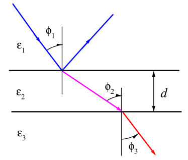
We assume that the permittivity of the intermediate layer is real (negligible absorption) and smaller than that of the surrounding media on both sides. The 3rd layer permittivity is . While we take and , no special relation between and is assumed. An exemplary structure we consider is a pair of semiconductor plates, optically coupled using an optical glue LED1 or a bonding oxide Bowers .
The solution for the amplitude reflectance, first obtained in Foester (see also e.g. BornWol , or L&L ), is of the form
| (1) |
Here and are the Fresnel reflection coefficients at the interfaces 1-2 and 2-3, respectively, and is the phase shift of the wave inside the film,
| (2) |
For a large one can define the total reflection angle by , which corresponds to the TIR for incident angles . When the phase shift is small, , the film is called optically thin; we note that close to the film is always optically thin.
The amplitude reflectance depends (through the reflection coefficients and ) on the polarization of light, which will be indicated below (when necessary) by an additional subscript. We shall use subscript for -polarized waves (electric field perpendicular to the plane of incidence) and for -polarization (electric field in the plane of incidence).
The Fresnel reflection coefficients for the two interfaces are given by
| (3) |
where and are interface indices: for the 1-2 interface and for the 2-3 interface, respectively. Note that ref .
Using Eqs. (1), (2), and (3), we calculate the reflection coefficient . The transmission coefficient for non-absorbing layer is then readily obtained as .
For small angles of incidence, , the phase shift and the interface reflection coefficients for both polarizations are real numbers (moreover, ), so that and we have
| (4) |
Equation (4) can be simplified using Fresnel’s equations and Snell’s refraction law, . After some algebra, the transmission coefficient can be brought into the form
| (5) |
where is the transmission coefficient of the interface 1-3. For a non-zero angle of incidence both and the coefficient are different for the two polarizations.
For -polarization we have:
| (6) |
and
| (7) |
Here and below we use the notation .
For -polarization we find:
| (8) |
and
| (9) |
Using some caution, one can apply Eq. (5) in the full range of variation of the angle of incidence, including the FTIR region (). In the FTIR region, the phase gain becomes imaginary, , where
| (10) |
while the reflection amplitudes become unimodular, . The reflection phase and other relevant phases can be readily written down using Fresnel’s equations. In the range of FTIR, the transmission coefficient is then given by CourtWil
| (11) |
where both and are given by the same Eqs. (6-9) but and become negative.
Note that the nature of reflection in the FTIR region, , is quite different, since the reflection coefficient from a single surface should be equal to unity. The complete single-surface reflection is frustrated by the interference with light reflected by the second surface, even though the field between the two surfaces has a totally evanescent character. For the optical field deeply penetrates into the interlayer. If , the transmission coefficient vanishes (and so does ) for , due to the TIR from layer 3.
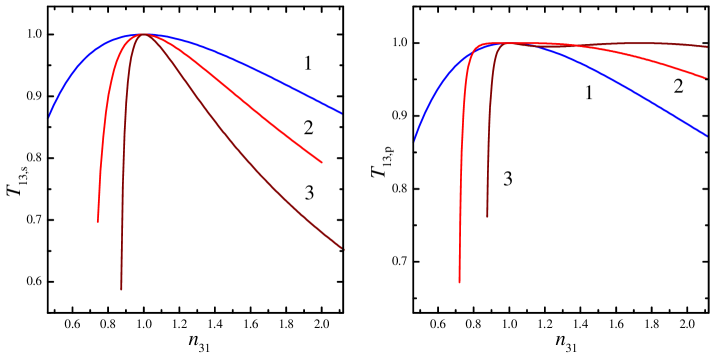
According to Eqs. (5) and (11), for a sufficiently thin film ( and ) the transmission coefficients approach , . These values in turn depend on and . The dependencies are presented in Fig. 2. For all incident angles the total transparency, , is reached only when . Away from the exact index matching the decrease of and is seen to be much steeper on the side . Since the exact matching of indices of the layers 1 and 3 is rarely possible, the structures with are preferable.
For small incidence angles, , one has a constructive interference between the waves in the middle layer, which results in the maximum of the transmission coefficient for both polarizations at , where is an integer, (for normal incidence this corresponds to ). Note that this anti-reflection effect arises for half-wave plates — rather than quarter-wave plates, which would be the case for an intermediate layer in structures with or . The almost total transparency of the film at is due to the phase shift in the reflection from the two film surfaces, which results in . The transmission coefficients in these interference maxima are given by and , Eqs. (7) and (9), respectively.
For normal incidence () one has , where
| (12) |
For most semiconductor pairs, the ratio is close to unity. For typical pairs with indices in the range of 3.5 to 4, the reflection losses at normal incidence are less than 0.5 %.
For an optically thin film, , one has
| (13) |
where and the reflection and transmission coefficients for the 1-2 and 2-3 interfaces are defined similar to , in Eq. (12). We see that the deviation .
For , the reflection coefficients go to unity, . This, however, does not imply , since one has at the same time. Therefore, one needs a more refined consideration of the reflection in the vicinity of . It is convenient to give expressions for the reciprocal transparencies in terms of the layer permittivities, viz.
| (14) |
and
| (15) |
For matching layers, , and -polarized waves, we have
| (16) |
Similarly, for matching layers and waves polarized in the plane of incidence
| (17) |
It follows from Eqs. (13), (16) and (17) that (i) for perpendicular () polarization, the reflection increases steadily as a function of the incidence angle, but it remains small up to the TIR angle; and (ii) the reflection for polarization is stronger than that for the parallel () polarization. The reflection of -polarized light is suppressed due to Brewster’s effect: for incidence at the Brewster angle, , one has (from Eq. 8) and the transmission (which equals unity for matching layers, ).
Note that for non-matching layers () there is a second Brewster angle, , corresponding to the wave in layer 2, propagating at the angle . One has when and the transmission increases again to . In terms of the incident wave angle this corresponds to . In the range of incidence angles (for ) or (in case ) one has and . Of course, the transmission does not exceed unity at any angle.
At the FTIR angle, , both and decrease at large as . Therefore, the widely used approximation, at and , works reasonably well for very thin interlayers (see Fig. 4 for and ) but it does not hold for thicker films [see Figs. 4 and 5, for and ].
Finally, for a thin interlayer with a finite absorption coefficient , transmission also decrease linearly with . However, for this is a negligible effect Abeles .
Higher-index overlayer
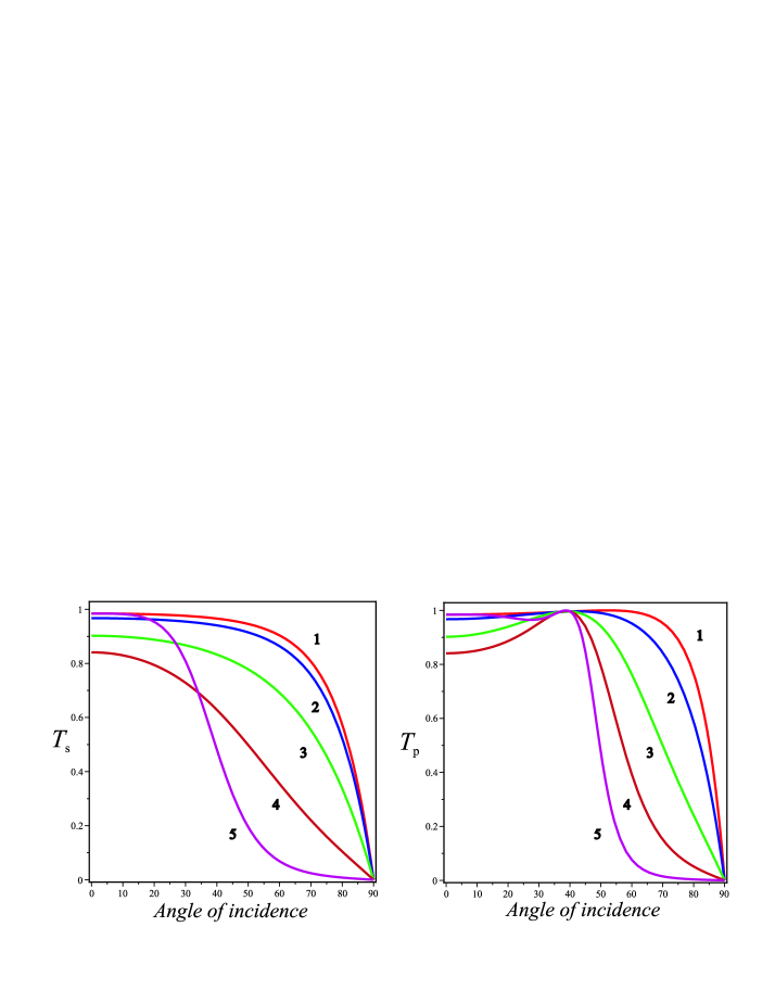
As the first example, we consider the transparency of a semiconductor structure consisting of two semiconductor layers (InAs and CdSb) having and , optically separated by a chalcogenide glass layer with . This example is close to parameters of mid-infrared LED opto-pairs comprising a light emitting diode and a lens attached to the diode by a layer of optical glue LED1 . Calculated dependencies of the transmission coefficient on the angle of incidence for two polarizations and four values of the layer thickness are shown in Figs. 3, in the angular range . For this example, the Brewster angles are =36.6∘ for the first surface and =40∘ for the second surface, so that the reflection of -polarized light is strongly suppressed even in the region close to the angle of TIR from the 1-2 surface, = 48∘.
For thicker interlayers, Figs. 3 show the growth of reflection for both polarizations in the region of total internal reflection. The reflection increases to unity at . For a half-wave plate the transparency is improved only in a range of angles of incidence smaller than the angle of TIR from the 1-2 interface.
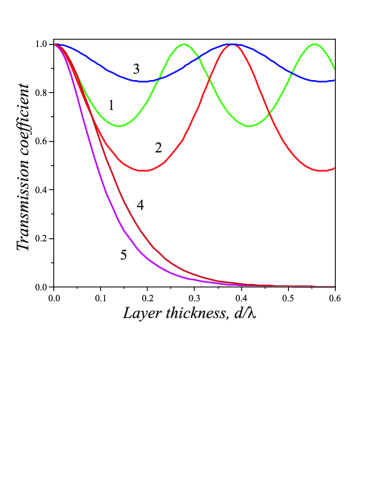
To ensure that the reflection losses at all angles of incidence are less than 10%, one needs to take . For example, in the mid-IR region ( 3 m) this gives 0.15 m, which is much more restrictive than usually expected.
Lower-index overlayer
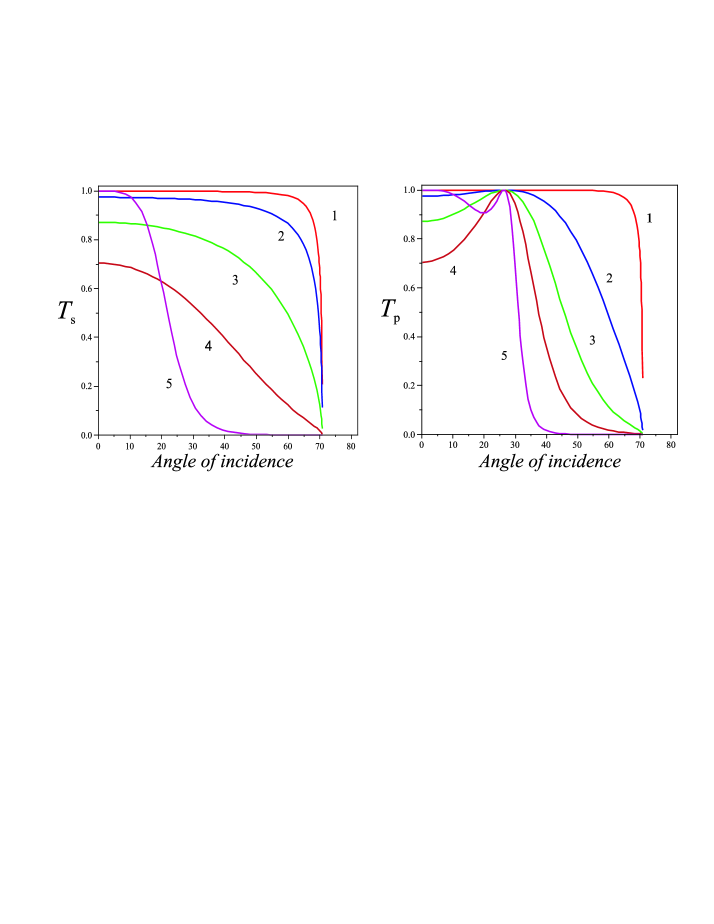
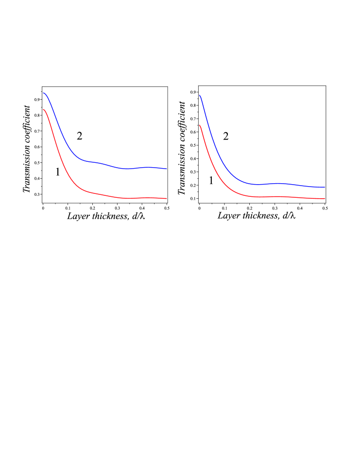
Another practical example is a bonded photodetector on top of a semiconductor scintillator slab with an optical-glue layer in between. We consider the interlayer transparency in a semiconductor structure consisting of GaAs layer 1 (emission 860 nm) with the index and InP photodiode layer 3 of index . The layers are optically separated by a layer with (which seems to be reasonable for the near-IR region). Figure 4 shows the transmission coefficients and , calculated as functions of the incidence angle for different interlayer thicknesses. Due to the high index contrast, the TIR angle from the interlayer is only . A smaller index of layer 3 () results in additional TIR and reduces the overall transparency region to . We note that the reflection losses are quite small for sufficiently thin films, as well as for -polarized waves at Brewster’s angle and for a “half-wavelength” thin film. The small reflection is, of course, owing to low index contrast between layers 1 and 3. Still, the requirements to the thickness of the interlayer in the near-infrared region are quite stringent. Even at small angles of incidence, one should use films with in order to reduce reflection losses below 10 %. For 860 nm, this corresponds to 50 nm, which is technologically challenging. Figure 5 shows the dependence of the transmission coefficients on the interlayer thickness in this structure for two polarizations and several angles of incidence, including the normal incidence and representative angles below and above . We clearly see the interference structure that is dependent on the angle of incidence and almost total transparency at the transmission maxima for .
A useful quantity to consider is the average transmission of optical power from an isotropic source, discussed in the next Section. As we shall see below, owing to the angular dependence of the transmission maxima positions, the average transmission is a monotonically decreasing function of the interlayer thickness.
Average transmitted power
The average optical power transmitted through the interlayer from a finite-size non-collimated source depends on the details of the geometry. Still, one can give meaningful definitions for the average in two limiting cases relevant to experimental applications (see Appendix). For radiation from a point-like source (isotropic non-polarized emission) the appropriate average transmission is of the form
| (18) |
Definition (18) corresponds to simple averaging of incident radiation over the solid angle and can be used to estimate the external efficiency of LED and scintillators when the emission layer is transparent, i.e. much thinner than the absorption length.
A different averaging procedure must be used for a distributed source whose linear dimensions (including the thickness) much exceed the absorption length. In this case, every small part of the surface is illuminated by an isotropic flux of radiation coming from the distance smaller than the absorption length. The common example of such a source is the quasi-equilibrium (homogeneous) interband luminescence of an optically excited semiconductor layer when the excitation region is much larger than the absorption length. The appropriate average in this case is of the form,
| (19) |
Definition (19) is implicitly used in the discussion of blackbody radiation (see e.g. L&L-StPh ). For non-equilibrium sources, an averaging procedure similar to (19) has been applied, e.g., to the situation when photon recycling dominates the source properties Yablon . In this case, owing to multiple photon absorption/re-emission processes, the radiation is widely distributed over the source layer.
We note that the average (19) is normalized (additional factor of 2 compared to Eq. 18) so that for a non-reflecting boundary one has . To compensate for this normalization factor, our expression for the average power transmission includes an additional factor of 0.5 (see Appendix). Since the transmission coefficients are decreasing functions of the incident angle , one can generally expect .
An interesting reciprocity relation can be proven for (but not for ), viz.
| (20) |
This “sum rule” follows from a thermodynamic equilibrium argument (see Appendix) and holds for any index and arbitrary thickness of the interlayer. In particular, the averaging in Eq. (20) includes the FTIR range of angles, where the interfaces 12 and 23 are totally reflective.
Figure 6 shows the average transmission coefficients and calculated for structures with both higher-index (left panel) and lower-index (right panel) overlayers. We see that for the decrease of the average transmission coefficients with is almost linear. The range of quadratic decrease that could be anticipated from Eq. (5) is extremely narrow. The origin of this can be traced back to analytical expressions. It is evident from Eqs. (18,19) that the contribution to the average of small angles of incidence is not decisive: the integrals for and receive little contribution from the angles where is much smaller than unity, and therefore the average transmission coefficients are very sensitive to the angular range where the transmission is high. With decreasing , the range of incidence angles where the film is highly transparent broadens as , see e.g. Fig. 4. As a result, for both polarizations, the decrease of with becomes linear rather than quadratic.
Summary and conclusions
We have analyzed the transparency of low-index intermediate layers between two higher-index semiconductor layers in the situation when the angular spread of incident radiation is important. The relevant applications we have in mind are semiconductor opto-pairs formed with an optical glue or adhesive.
Transmission of isotropic radiation by thin interlayers with low refractive index depends on the frustrated total internal reflection due to the constructive interference of evanescent waves reflected by the two surfaces of the interlayer. The main contribution to the average optical power transmission comes from fairly large angles of incidence. This implies a significant reflection loss even for thin films of thickness less than the wavelength. For the typical thicknesses (m) of the optical glue interlayers the losses are high even in the mid-infrared region.
In light of our results, even the best (thinnest) reported oxide layers used for optical wafer bonding may not be sufficiently thin for some intended applications. Consider the record-thin 60 nm oxide bonding layer, recently reported by Bowers . For the case of InP photodiode structure with SiO2 bonding layer of index 1.46 one has the parameter and the reflection is strong for all angles. To ensure reasonable power transmission across the bonding layer one must have its thickness well below , which may be quite challenging technologically.
Special attention has been paid to the angular average of the optical power transmission, which is shown to possess a universal form for two practically relevant classes of source layers. We have found a simple and universal sum rule that must be satisfied by the angular dependence of the transmission coefficient. The sum rule has the form of reciprocal relation (20) and holds for three-layer structures with non-absorbing interlayers of arbitrary thickness and refractive index. It also demonstrates that the average transmission coefficient of the three-layer structure is sensitive to the overlayer refractive index relative to that of the source layer and that structures with larger overlayer index are preferable.
Acknowledgements
We are grateful to Sergey Suchalkin for useful discussions. This work has been supported by the Domestic Nuclear Detection Office (DNDO) of the Department of Homeland Security, by the Defense Threat Reduction Agency (DTRA) through its basic research program, and by the New York State Office of Science, Technology and Academic Research (NYSTAR) through the Center for Advanced Sensor Technology (Sensor CAT) at Stony Brook.
APPENDIX. Equilibrium radiation and transmitted luminescence
In general, radiation transmitted through a multi-layered semiconductor structure may strongly depend on the details of geometry, especially in case when the linear dimensions of the emitting region are comparable to the wavelength or the absorption length. In this situation, one may need detailed modeling that takes into account the boundary effects. However, there are two limiting cases when boundary effects are not important. Fortunately, these limiting cases are precisely those that are most relevant for applications to semiconductor opto-electronic devices in the visible and near-infrared range.
The first case corresponds to a transparent emitting layer of large area and a finite thickness that is substantially smaller than the absorption length. The second case corresponds to the opposite limit of interband emission by thick absorbing layers of linear dimensions much larger than the absorption length. In both limits the transmission assumes a universal – albeit different – form.
Consider first a transparent layer 1 with a point-like isotropic source of power located at a distance from the layer surface. The normal component of the incident flux through a circular area at the surface (where ) is , where is the solid angle of illumination of the area . Therefore, in this case the average transmission coefficient for the power transmitted to material 3 (through an intermediate layer 2) should be defined as follows:
| (A.1) |
It is important to note that the transmitted power does not depend on and hence the same average transmission coefficient (A.1) determines the transparency of a unit area of the surface layer for the case when the source of radiation is distributed in a layer of large area and finite thickness.
The other limiting case is radiation escape from an absorbing layer. Consider as an example the total power of equilibrium radiation emitted at a temperature by a homogeneous and optically isotropic material 1. The rate of radiation emission obeys the detailed balance between the emission and absorption processes embodied in the van Roosbroeck-Shockley relation VRS and is proportional to the absorption coefficient . The photon density in the unit frequency interval at emitted in unit volume per unit time is given by Moss
| (A.2) |
On its way out the radiation may be absorbed and re-emitted many times, but this does not change the equilibrium photon density. The number of photons reaching the surface unit at distance from the emitting source in volume equals
| (A.3) |
At a given incidence angle , the distance to the surface . Therefore the total photon flux to the unit surface (at ) from the region in a unit solid angle about a fixed incidence angle can be obtained by integration over , which takes the form
| (A.4) |
where is the equilibrium photon density of thermal radiation and is the speed of light in the emitting material. Since the integral in the right-hand side of Eq. (A.4) equals unity, the Eq. (A.4) shows that the equilibrium flux to the surface is identical to blackbody radiation and depends neither on the incidence angle nor on the particular shape of (weak emission rate in frequency regions of small absorption is compensated by the high material transparency at these frequencies). The energy transmitted to material 3 is given by the integral over the normal component of the incident flux, multiplied by the transmission coefficient , i.e.
| (A.5) |
where we have suppressed the frequency index , since Eq. (A.5) is valid for each frequency individually. For it gives a well-known result . For we can define the average transmission coefficient from 1 to 3 by
| (A.6) |
so that .
Note that the shape of Eq. (A.5) derives from the fact that the integral in (A.4) is independent of , and therefore it remains valid for a layer of finite thickness, so long as it much exceeds the absorption length . Therefore, the average (A.6) can be used to quantify the surface transparency in the case of a quasi-equilibrium emission (e.g. optically excited luminescence) from an absorbing region, so long as than both its thickness and lateral extent are larger than the absorption length. For a non-reflective surface , while for an interlayer with finite reflection , since generally is a decreasing function of .
We remark that the two averaging procedures lead to tangible differences in power transmission only when the radiation goes through a large solid angle. The difference is therefore of the essence for opto-pairs we are interested in, where the refractive indices and are not vastly disparate. In contrast, for emission from a semiconductor to low-index media (such as air or vacuum) the transmission is restricted by the TIR to small angles and the difference in power transmission is minor simple .
Consider now the case of thermal equilibrium between material 1 and material 3. For the equilibrium to hold, one should have . This requires that
| (A.7) |
Suppose . Part of the equilibrium radiation incident on the interface gets reflected due to the TIR phenomenon. However, this is exactly compensated by the higher density of photon states in the higher-index material. This compensation is “moderated” by the slower velocity of the energy flux in the second material, so that the resultant compensating effect is of the second, and not the third power in . Obviously, for a non-equilibrium situation there is no compensation. But the sum rule expressed by Eq. (A.7) remains valid, so that the calculated transmission coefficient must obey Eq. (A.7).
The sum rule (A.7) holds for any planar interface including any intermediate layer of index , so long as there is no absorption in the intermediate layer. This can be verified by direct inspection of the integrals using explicit expressions (5) for both polarizations. To do this, we note that the transmission coefficients and can be written as functions of both the incidence angle and the refraction angle, subject to Snell’s law , that holds for both directions of transmission. As an example, we can write in the form
| (A.8) |
that makes symmetry between transmission coefficients 13 and 31 evident. Similarly, can be written as where
| (A.9) |
and the phase shift as . Then, one can replace integration in the left-hand side of Eq. (A.7) over by integration over so that or, with Snell’s law,
| (A.10) |
Finally, by changing the integration variable from to (with an appropriate change of the integration interval), we arrive at the direct proof of the sum rule (A.7).
References
- (1) T. S. Moss, G. J. Burrell, and B. Ellis, Semiconductor Opto-Electronics, Butterworth & Co, Ltd, (1973).
- (2) D. Delbeke, R. Bockstaele, P. Bienstman, R. Baets, and H. Benisty, “High-efficiency semiconductor resonant-cavity light-emitting diodes: A review,” IEEE J. Quantum Electron. 8, 189-206 (2002).
- (3) M. A. Remennyi, N.V. Zotova, A. A. Kardashev, B. A. Matveev, N. M. Stus’, and G. N. Talalakin, “Low voltage episide down bonded mid-IR diode optopairs for gas sensing in the 3.3-4.3 m spectral range,” Sensors and Actuators B 91, 256-261 (2003).
- (4) H. Gauck, T. H. Gfroerer, M. J. Rean, E. A. Cornell, and K. A. Bertness, “External radiative quantum efficiency of 96 % from a GaAs/GaInP heterostructure,” Appl. Phys. A, 143-147 (1997).
- (5) A. A. Kastalsky, S. Luryi, and B. Spivak, “Semiconductor high-energy radiation scintillator detector,” Nucl. Instr. and Meth. A 565, 650-656 (2006).
- (6) Di Liang, A. W. Fang, H. Park, T. E. Reynolds, K. Warner, D. C. Oakley, and J. E. Bowers, “Low temperature, Strong SiO2-SiO2 Covalent Wafer Bonding for III-V Compound Semiconductors-to-Silicon Photonic Integrated Circuits,” J. Electronic Materials 37, 1552-1559 (2008).
- (7) The review of the history and some applications of FTIR can be found in: S. Zhu, A. W. Yu, D. Hawley, and R. Roy, “Frustrated total internal reflection: A demonstration and review,” Am. J. Phys. 54, 601-607 (1986).
- (8) K. Foesterling, “Uber die Messung der Optishen Konstanten sehr dünner Metallschichten,” Ann. Phys. 30, 745 (1937).
- (9) M. Born and E. Wolf, Principles of Optics (Pergamon, Oxford, 1980), Sec 1.6.4.
- (10) L. D. Landau and E. M. Lifshitz, Electrodynamics of Continuous Media (Pergamon, Oxford, 1984).
- (11) We remark that Eqs. (3) evaluated at produce an opposite sign for the amplitude reflection coefficients of - and -polarized waves, even though at normal incidence these waves are identical. It should be noted that reflection coefficients for and polarizations are written down in (3) in terms of the electric and the magnetic fields, respectively. The negative sign for the -polarized wave originates from the phase difference in the reflected wave.
- (12) F. Abelès, “Optical Properties of Thin Absorbing Films,” J. Opt. Soc. Am. 47, 473-482 (1957).
- (13) I. N. Court and F. K. Willisen, “Frustrated Total Internal Reflection and Application of its Principle to Laser Cavity Design,” Appl. Opt. , 3, 719 - 726 (1964).
- (14) W. van Roosbroeck and W. Shockley, “Photon-radiative recombination of electrons and holes in Germanium,” Phys. Rev. 94, 1558-1560 (1954).
- (15) L. D. Landau and E. M. Lifshitz, Statistical Physics, 3rd Edition, Part 1 (Pergamon, Oxford, 1984).
- (16) I. Schnitzer, E. Yablonovitch, C. Caneau, and T.J. Gmitter, “Ultrahigh spontaneous quantum efficiency, 99.7 % internally and 72 % externally, from AlGaAs/GaAs/ AlGaAs double heterostructure,” Appl. Phys. Lett. 81, 131-133 (1993).
- (17) For emission into vacuum from a semiconductor with , the transmitted fraction of optical power (restricted only by the total internal reflection) can be estimated as for both averaging procedures.