NATURE 452, 970 (2008) [News & Views at NAT.PHYS. 4, 348 (2008)]
A topological Dirac insulator in a quantum spin Hall phase
When electrons are subject to a large external magnetic field, the conventional charge quantum Hall effect Klitzing ; Tsui dictates that an electronic excitation gap is generated in the sample bulk, but metallic conduction is permitted at the boundary. Recent theoretical models suggest that certain bulk insulators with large spin-orbit interactions may also naturally support conducting topological boundary states in the extreme quantum limit Kane(Graphene) ; Bernevig(QSHE) ; Sheng(QSHE) , which opens up the possibility for studying unusual quantum Hall-like phenomena in zero external magnetic fields Haldane(P-anomaly) . Bulk Bi1-xSbx single crystals are predicted to be prime candidates Fu:STI1 ; Murukami for one such unusual Hall phase of matter known as the topological insulator Fu:STI2 ; Moore:STI1 ; Roy . The hallmark of a topological insulator is the existence of metallic surface states that are higher dimensional analogues of the edge states that characterize a quantum spin Hall insulator Kane(Graphene) ; Bernevig(QSHE) ; Sheng(QSHE) ; Haldane(P-anomaly) ; Fu:STI1 ; Murukami ; Fu:STI2 ; Moore:STI1 ; Roy ; Bernevig:HgTe ; Konig . In addition to its interesting boundary states, the bulk of Bi1-xSbx is predicted to exhibit three-dimensional Dirac particles Wolff ; Fukuyama ; Buot ; Lenoir , another topic of heightened current interest following the new findings of two-dimensional graphene Zhang ; Novoselov ; Zhou and charge quantum Hall fractionalization observed in pure bismuth Behnia . However, despite numerous transport and magnetic measurements on the Bi1-xSbx family since the 1960s Lenoir , no direct evidence of either topological quantum Hall-like states or bulk Dirac particles has ever been found. Here, using incident-photon-energy-modulated angle-resolved photoemission spectroscopy (IPEM-ARPES), we report the direct observation of massive Dirac particles in the bulk of Bi0.9Sb0.1, locate the Kramers’ points at the sample’s boundary and provide a comprehensive mapping of the topological Dirac insulator’s gapless surface modes. These findings taken together suggest that the observed surface state on the boundary of the bulk insulator is a realization of the much sought exotic “topological metal” Fu:STI2 ; Moore:STI1 ; Roy . They also suggest that this material has potential application in developing next-generation quantum computing devices that may incorporate “light-like” bulk carriers and topologically protected spin-textured edge-surface currents.
Bismuth is a semimetal with strong spin-orbit interactions. Its band structure is believed to feature an indirect negative gap between the valence band maximum at the T point of the bulk Brillouin zone (BZ) and the conduction band minima at three equivalent L points Lenoir ; Liu (here we generally refer to these as a single point, L). The valence and conduction bands at L are derived from antisymmetric (La) and symmetric (Ls) -type orbitals, respectively, and the effective low-energy Hamiltonian at this point is described by the (3+1)-dimensional relativistic Dirac equation Wolff ; Fukuyama ; Buot . The resulting dispersion relation, , is highly linear owing to the combination of an unusually large band velocity and a small gap (such that Å-1) and has been used to explain various peculiar properties of bismuth Wolff ; Fukuyama ; Buot . Substituting bismuth with antimony is believed to change the critical energies of the band structure as follows (see Fig.1). At an Sb concentration of , the gap between La and Ls closes and a massless three-dimensional (3D) Dirac point is realized. As is further increased this gap re-opens with inverted symmetry ordering, which leads to a change in sign of at each of the three equivalent L points in the BZ. For concentrations greater than there is no overlap between the valence band at T and the conduction band at L, and the material becomes an inverted-band insulator. Once the band at T drops below the valence band at L, at , the system evolves into a direct-gap insulator whose low energy physics is dominated by the spin-orbit coupled Dirac particles at L Fu:STI1 ; Lenoir .
Recently, semiconductors with inverted band gaps have been proposed to manifest the two-dimensional (2D) quantum spin Hall phase, which is predicted to be characterized by the presence of metallic 1D edge states Kane(Graphene) ; Bernevig(QSHE) ; Sheng(QSHE) ; Bernevig:HgTe . Although a band-inversion mechanism and edge states have been invoked to interpret the transport results in 2D mercury telluride semiconductor quantum wells Konig , no 1D edge states are directly imaged, so their topological character is unknown. Recent theoretical treatments Fu:STI1 ; Murukami have focused on the strongly spin-orbit coupled, band-inverted Bi1-xSbx series as a possible 3D bulk realization of the quantum spin Hall phase in which the 1D edge states are expected to take the form of 2D surface states Fu:STI1 ; Murukami ; Fu:STI2 that may be directly imaged and spectroscopically studied, making it feasible to identify their topological order parameter character. Most importantly, the 3D phase is a new phase of matter in terms of its topological distinctions Moore:STI1 .
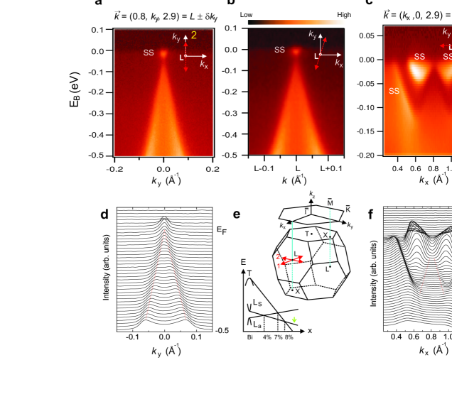
High-momentum-resolution angle-resolved photoemission spectroscopy performed with varying incident photon energy (IPEM-ARPES) allows for measurement of electronic band dispersion along various momentum space (-space) trajectories in the 3D bulk BZ. ARPES spectra taken along two orthogonal cuts through the L point of the bulk BZ of Bi0.9Sb0.1 are shown in Figs 1a and c. A -shaped dispersion whose tip lies less than 50 meV below the Fermi energy () can be seen along both directions. Additional features originating from surface states that do not disperse with incident photon energy are also seen. Owing to the finite intensity between the bulk and surface states, the exact binding energy () where the tip of the -shaped band dispersion lies is unresolved. The linearity of the bulk -shaped bands is observed by locating the peak positions at higher in the momentum distribution curves (MDCs), and the energy at which these peaks merge is obtained by extrapolating linear fits to the MDCs. Therefore 50 meV represents a lower bound on the energy gap between La and Ls. The magnitude of the extracted band velocities along the and directions are ms-1 and ms-1, respectively, which are similar to the tight binding values ms-1 and ms-1 calculated for the La band of bismuth Liu . Our data are consistent with the extremely small effective mass of (where is the electron mass) observed in magneto-reflection measurements on samples with Hebel . The Dirac point in graphene, co-incidentally, has a band velocity ( ms-1) Zhang comparable to what we observe for Bi0.9Sb0.1, but its spin-orbit coupling is several orders of magnitude weaker Kane(Graphene) , and the only known method of inducing a gap in the Dirac spectrum of graphene is by coupling to an external chemical substrate Zhou . The Bi1-xSbx series thus provides a rare opportunity to study relativistic Dirac Hamiltonian physics in a 3D condensed matter system where the intrinsic (rest) mass gap can be easily tuned.
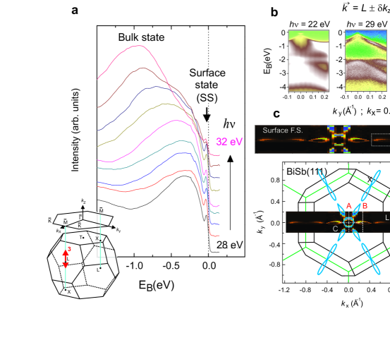
Studying the band dispersion perpendicular to the sample surface provides a way to differentiate bulk states from surface states in a 3D material. To visualize the near- dispersion along the 3D L-X cut (X is a point that is displaced from L by a distance of 3, where is the lattice constant), in Fig.2a we plot energy distribution curves (EDCs), taken such that electrons at have fixed in-plane momentum = (Lx, Ly) = (0.8 Å-1, 0.0 Å-1), as a function of photon energy (). There are three prominent features in the EDCs: a non-dispersing, independent, peak centered just below at about 0.02 eV; a broad non-dispersing hump centered near 0.3 eV; and a strongly dispersing hump that coincides with the latter near = 29 eV. To understand which bands these features originate from, we show ARPES intensity maps along an in-plane cut (parallel to the direction) taken using values of 22 eV, 29 eV and 35 eV, which correspond to approximate values of L 0.3 Å-1, Lz, and Lz + 0.3 Å-1 respectively (Fig.2b). At = 29 eV, the low energy ARPES spectral weight reveals a clear -shaped band close to . As the photon energy is either increased or decreased from 29 eV, this intensity shifts to higher binding energies as the spectral weight evolves from the -shaped into a -shaped band. Therefore the dispersive peak in Fig.2a comes from the bulk valence band, and for = 29 eV the high symmetry point L = (0.8, 0, 2.9) appears in the third bulk BZ. In the maps of Fig.2b with respective values of 22 eV and 35 eV, overall weak features near that vary in intensity remain even as the bulk valence band moves far below . The survival of these weak features over a large photon energy range (17 to 55 eV) supports their surface origin. The non-dispersing feature centered near eV in Fig.2a comes from the higher binding energy (valence band) part of the full spectrum of surface states, and the weak non-dispersing peak at eV reflects the low energy part of the surface states that cross away from the point and forms the surface Fermi surface (Fig.2c).
Having established the existence of an energy gap in the bulk state of Bi0.9Sb0.1 (Figs 1 and 2) and observed linearly dispersive bulk bands uniquely consistent with strong spin-orbit coupling model calculations Wolff ; Fukuyama ; Buot ; Liu (see Supplementary Information for full comparison with theoretical calculation), we now discuss the topological character of its surface states, which are found to be gapless (Fig.2c). In general, the states at the surface of spin-orbit coupled compounds are allowed to be spin split owing to the loss of space inversion symmetry . However, as required by Kramers’ theorem, this splitting must go to zero at the four time reversal invariant momenta (TRIM) in the 2D surface BZ. As discussed in Fu:STI1 ; Fu:STI2 , along a path connecting two TRIM in the same BZ, the Fermi energy inside the bulk gap will intersect these singly degenerate surface states either an even or odd number of times. When there are an even number of surface state crossings, the surface states are topologically trivial because weak disorder (as may arise through alloying) or correlations can remove pairs of such crossings by pushing the surface bands entirely above or below . When there are an odd number of crossings, however, at least one surface state must remain gapless, which makes it non-trivial Fu:STI1 ; Murukami ; Fu:STI2 . The existence of such topologically non-trivial surface states can be theoretically predicted on the basis of the bulk band structure only, using the invariant that is related to the quantum Hall Chern number Kane(QSHE-Z2) . Materials with band structures with are ordinary Bloch band insulators that are topologically equivalent to the filled shell atomic insulator, and are predicted to exhibit an even number (including zero) of surface state crossings. Materials with bulk band structures with on the other hand, which are expected to exist in rare systems with strong spin-orbit coupling acting as an internal quantizing magnetic field on the electron system Haldane(P-anomaly) , and inverted bands at an odd number of high symmetry points in their bulk 3D BZs, are predicted to exhibit an odd number of surface state crossings, precluding their adiabatic continuation to the atomic insulator Kane(Graphene) ; Fu:STI1 ; Murukami ; Fu:STI2 ; Moore:STI1 ; Roy ; Bernevig:HgTe ; Konig . Such “topological quantum Hall metals” Fu:STI2 ; Moore:STI1 ; Roy cannot be realized in a purely 2D electron gas system such as the one realized at the interface of GaAs/GaAlAs systems.
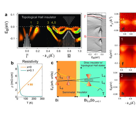
In our experimental case, namely the (111) surface of Bi0.9Sb0.1, the four TRIM are located at and three points that are rotated by relative to one another. Owing to the three-fold crystal symmetry (A7 bulk structure) and the observed mirror symmetry of the surface Fermi surface across (Fig.2), these three points are equivalent (and we henceforth refer to them as a single point, ). The mirror symmetry is also expected from time reversal invariance exhibited by the system. The complete details of the surface state dispersion observed in our experiments along a path connecting and are shown in Fig.3a; finding this information is made possible by our experimental separation of surface states from bulk states. As for bismuth (Bi), two surface bands emerge from the bulk band continuum near to form a central electron pocket and an adjacent hole lobe Ast:Bi1 ; Hochst ; Hofmann . It has been established that these two bands result from the spin-splitting of a surface state and are thus singly degenerate Hirahara ; Hofmann . On the other hand, the surface band that crosses at Å-1, and forms the narrow electron pocket around , is clearly doubly degenerate, as far as we can determine within our experimental resolution. This is indicated by its splitting below between Å-1 and , as well as the fact that this splitting goes to zero at in accordance with Kramers theorem. In semimetallic single crystal bismuth, only a single surface band is observed to form the electron pocket around Hengsberger ; Ast:Bi2 . Moreover, this surface state overlaps, hence becomes degenerate with, the bulk conduction band at L (L projects to the surface point) owing to the semimetallic character of Bi (Fig.3b). In Bi0.9Sb0.1 on the other hand, the states near fall completely inside the bulk energy gap preserving their purely surface character at (Fig.3a). The surface Kramers doublet point can thus be defined in the bulk insulator (unlike in Bi Hirahara ; Ast:Bi1 ; Hochst ; Hofmann ; Hengsberger ; Ast:Bi2 ) and is experimentally located in Bi0.9Sb0.1 samples to lie approximately 15 5 meV below at (Fig.3a). For the precise location of this Kramers point, it is important to demonstrate that our alignment is strictly along the line. To do so, we contrast high resolution ARPES measurements taken along the line with those that are slightly offset from it (Fig.3e). Figs 3f-i show that with offset from the Kramers point at by less than 0.02 Å-1, the degeneracy is lifted and only one band crosses to form part of the bow-shaped electron distribution (Fig.3d). Our finding of five surface state crossings (an odd rather than an even number) between and (Fig.3a), confirmed by our observation of the Kramers degenerate point at the TRIM, indicates that these gapless surface states are topologically non-trivial. This corroborates our bulk electronic structure result that Bi0.9Sb0.1 is in the insulating band-inverted () regime (Fig.3c), which contains an odd number of bulk (gapped) Dirac points, and is topologically analogous to an integer quantum spin Hall insulator.
Our experimental results taken collectively strongly suggest that Bi0.9Sb0.1 is quite distinct from graphene Zhang ; Novoselov and represents a novel state of quantum matter: a strongly spin-orbit coupled insulator with an odd number of Dirac points with a negative topological Hall phase, which realizes the “parity anomaly without Fermion doubling”. Our work further demonstrates a general methodology for possible future investigations of novel topological orders in exotic quantum matter.
Note Added : In a very recent work we have successfully imaged the spin-polarization of the topological edge modes using high-resolution spin-resolved-ARPES Science .
Acknowledgements We thank P. W. Anderson, B. A. Bernevig, F. D. M. Haldane, D. A. Huse, C. L. Kane, R. B. Laughlin, N. P. Ong, A. N. Pasupathy and D. C. Tsui for discussions. This work is supported by the DOE Office of Basic Energy Science and materials synthesis is supported by the NSF MRSEC.
Author information Correspondence and requests for materials should be addressed to M.Z.H (mzhasan@princeton.edu).
I Methods
High resolution IPEM-ARPES data have been taken at Beamlines 12.0.1 and 10.0.1 of the Advanced Light Source in Lawrence Berkeley National Laboratory, as well as at PGM Beamline of the Synchrotron Radiation Center in Wisconsin, with photon energies from 17 to 55 eV and energy resolution from 9 to 40 meV and momentum (k-)resolution better than of the surface Brillouin zone. Data were taken on high quality bulk single crystal Bi1-xSbx at a temperature of 15 K and chamber pressures better than torr. Throughout this paper, the bulk bands presented are from those measured in the third bulk Brillouin zone to ensure a high degree of signal-to-noise contrast, and the values are estimated using the standard free-electron final state approximation.
References
- (1) von Klitzing, K., Dorda, G. & Pepper, M. New method for high-accuracy determination of the fine-structure constant based on quantized Hall resistance. Phys. Rev. Lett. 45, 494-497 (1980).
- (2) Tsui, D.C., Stormer, H.L. & Gossard, A.C. Two-dimensional magnetotransport in the extreme quantum limit. Phys. Rev. Lett. 48, 1559-1562 (1982).
- (3) Kane, C.L. & Mele, E.J. Quantum spin Hall effect in graphene. Phys. Rev. Lett. 95, 226801 (2005).
- (4) Bernevig, B.A. & Zhang, S.-C. Quantum spin Hall effect. Phys. Rev. Lett. 96, 106802 (2006).
- (5) Sheng, D.N., Weng, Z.Y., Sheng, L. & Haldane, F.D.M. Quantum spin Hall effect and topological Chern numbers. Phys. Rev. Lett. 97, 036808 (2006).
- (6) Haldane, F.D.M. Model for a quantum Hall effect without Landau levels: Condensed-matter realization of the “parity anomaly”. Phys. Rev. Lett. 61, 2015-2018 (1988).
- (7) Fu, L. & Kane, C.L. Topological insulators with inversion symmetry. Phys. Rev. B76, 045302 (2007).
- (8) Murakami, S. Phase transition between the quantum spin Hall and insulator phases in 3D: emergence of a topological gapless phase. New. J. Phys. 9, 356 (2007).
- (9) Fu, L., Kane, C.L. & Mele, E.J. Topological insulators in three dimensions. Phys. Rev. Lett. 98, 106803 (2007).
- (10) Moore, J.E. & Balents, L. Topological invariants of time-reversal-invariant band structures. Phys. Rev. B75, 121306(R) (2007).
- (11) Roy, R. Three dimensional topological invariants for time reversal invariant Hamiltonians and the three dimensional quantum spin Hall effect. Preprint at http://arxiv.org/abs/cond-mat/0607531 (2006).
- (12) Bernevig, B.A., Hughes, T.L. & Zhang, S.-C. Quantum spin Hall effect and topological phase transition in HgTe quantum wells. Science 314, 1757-1761 (2006).
- (13) König, M. et al. Quantum spin Hall insulator state in HgTe quantum wells. Science 318, 766-770 (2007).
- (14) Wolff, P.A. Matrix elements and selection rules for the two-band model of bismuth. J. Phys. Chem. Solids 25, 1057-1068 (1964).
- (15) Fukuyama, H. & Kubo, R. Interband effects of magnetic susceptibility. II. Diamagnetism of bismuth. J. Phys. Soc. Jpn. 28, 570-581 (1970).
- (16) Buot, F.A. Weyl transformation and the magnetic susceptibility of a relativistic Dirac electron gas. Phys. Rev. A8, 1570-1581 (1973).
- (17) Lenoir, B. et al. Bi-Sb alloys: an update. Fifteenth International Conference on Thermoelectrics, 1-13 (1996).
- (18) Zhang, Y. et.al. Experimental observation of the quantum Hall effect and Berry’s phase in graphene. Nature 438, 201-204 (2005).
- (19) Novoselov, K.S. et al. Room temperature quantum Hall effect in graphene. Science 315, 1379 (2007).
- (20) Zhou, S.Y. et al. Substrate-induced bandgap opening in epitaxial graphene. Nature Mat. 6, 770-775 (2007).
- (21) Behnia, K., Balicas, L. & Kopelevich, Y. Signatures of electron fractionalization in ultraquantum bismuth. Science 317, 1729-1731 (2007).
- (22) Liu, Y. & Allen, E. Electronic structure of semimetals Bi and Sb. Phys. Rev. B52, 1566-1577 (1995).
- (23) Hebel, L.C. & Smith, G.E. Interband transitions and band structure of a BiSb alloy. Phys. Lett. 10, 273-275 (1964).
- (24) Kane, C.L. & Mele, E.J. topological order and the quantum spin Hall effect. Phys. Rev. Lett. 95, 246802 (2005).
- (25) Ast, C.R. & Hochst, H. Fermi Surface of Bi(111) Measured by Photoemission Spectroscopy. Phys. Rev. Lett. 87, 177602 (2001).
- (26) Hochst, H. & Gorovikov, S. Lack of electron-phonon coupling along two-dimensional bands in Bi1-xSbx single crystal alloys. J. Elect. Spectrosc. Relat. Phenom. 351, 144-147 (2005).
- (27) Hofmann, P. The surfaces of bismuth: Structural and electronic properties. Prog. Surf. Sci. 81, 191-245 (2006).
- (28) Hirahara, T. et al. Direct observation of spin splitting in bismuth surface states. Phys. Rev. B76, 153305 (2007).
- (29) Hengsberger, M. et al. Photoemission study of the carrier bands in Bi(111). Eur. Phys. J. 17, 603-608 (2000).
- (30) Ast, C.R. & Hochst, H. Electronic structure of a bismuth bilayer. Phys. Rev. B67, 113102 (2003).
- (31) Hsieh, D., Hasan, M.Z. et al. Probing the spin degrees of freedom of a quantum spin Hall insulator. Science (accepted, in-press) (2009).
Figure 1. Dirac-like dispersion near the L point in the bulk Brillouin zone. Selected ARPES intensity maps of Bi0.9Sb0.1 are shown along three -space cuts through the L point of the bulk 3D Brillouin zone (BZ). The presented data are taken in the third BZ with Lz = 2.9 Å-1 with a photon energy of 29 eV. The cuts are along a, the direction, b, a direction rotated by approximately from the direction, and c, the direction. Each cut shows a -shaped bulk band whose tip lies below the Fermi level signalling a bulk gap. The surface states are denoted SS and are all identified in Fig.2 (for further identification via theoretical calculations see Supplementary Information). d, Momentum distribution curves (MDCs) corresponding to the intensity map in a. f, Log scale plot of the MDCs corresponding to the intensity map in c. The red lines are guides to the eye for the bulk features in the MDCs. e, Schematic of the bulk 3D BZ of Bi1-xSbx and the 2D BZ of the projected (111) surface. The high symmetry points , and of the surface BZ are labeled. Schematic evolution of bulk band energies as a function of is shown. The L band inversion transition occurs at , where a 3D gapless Dirac point is realized, and the composition we study here (for which ) is indicated by the green arrow. A more detailed phase diagram based on our experiments is shown in Fig.3c.
Figure 2. Dispersion along the cut in the -direction. Surface states are experimentally identified by studying their out-of-plane momentum dispersion through the systematic variation of incident photon energy. a, Energy distribution curves (EDCs) of Bi0.9Sb0.1 with electrons at the Fermi level () maintained at a fixed in-plane momentum of (=0.8 Å-1, =0.0 Å-1) are obtained as a function of incident photon energy to identify states that exhibit no dispersion perpendicular to the (111)-plane along the direction shown by the double-headed arrow labeled “3” in the inset (see Methods for detailed procedure). Selected EDC data sets with photon energies of 28 eV to 32 eV in steps of 0.5 eV are shown for clarity. The non-energy dispersive ( independent) peaks near are the surface states (SS). b, ARPES intensity maps along cuts parallel to taken with electrons at fixed at = 0.8 Å-1 with respective photon energies of = 22 eV, 29 eV and 35 eV (for a conversion map from photon energy to see Supplementary Information). The faint -shaped band at = 22 eV and = 35 eV shows some overlap with the bulk valence band at L ( = 29 eV), suggesting that it is a resonant surface state degenerate with the bulk state in some limited k-range near . The flat band of intensity centered about 2 eV in the = 22 eV scan originates from Bi 5d core level emission from second order light. c, Projection of the bulk BZ (black lines) onto the (111) surface BZ (green lines). Overlay (enlarged in inset) shows the high resolution Fermi surface (FS) of the metallic SS mode, which was obtained by integrating the ARPES intensity (taken with = 20 eV) from 15 meV to 10 meV relative to . The six tear-drop shaped lobes of the surface FS close to (center of BZ) show some intensity variation between them that is due to the relative orientation between the axes of the lobes and the axis of the detector slit. The six-fold symmetry was however confirmed by rotating the sample in the plane. EDCs corresponding to the cuts A, B and C are also shown; these confirm the gapless character of the surface states in bulk insulating Bi0.9Sb0.1.
Figure 3. The topological gapless surface states in bulk insulating Bi0.9Sb0.1. a, The surface band dispersion second derivative image (SDI) of Bi0.9Sb0.1 along . The shaded white area shows the projection of the bulk bands based on ARPES data, as well as a rigid shift of the tight binding bands to sketch the unoccupied bands above the Fermi level. To maintain high momentum resolution, data were collected in two segments of momentum space, then the intensities were normalized using background level above the Fermi level. A non-intrinsic flat band of intensity near generated by the SDI analysis was rejected to isolate the intrinsic dispersion. The Fermi crossings of the surface state are denoted by yellow circles, with the band near Å-1 counted twice owing to double degeneracy. The red lines are guides to the eye. An in-plane rotation of the sample by produced the same surface state dispersion. The EDCs along are shown to the right. There are a total of five crossings from which indicates that these surface states are topologically non-trivial. The number of surface state crossings in a material (with an odd number of Dirac points) is related to the topological invariant (see text). b, The resistivity curves of Bi and Bi0.9Sb0.1 reflect the contrasting transport behaviours. The presented resistivity curve for pure bismuth has been multiplied by a factor of 80 for clarity. c, Schematic variation of bulk band energies of Bi1-xSbx as a function of (based on band calculations and on Fu:STI1 ; Lenoir ). Bi0.9Sb0.1 is a direct gap bulk Dirac point insulator well inside the inverted-band regime, and its surface forms a “topological metal” - the 2D analogue of the 1D edge states in quantum spin Hall systems. d, ARPES intensity integrated within meV of originating solely from the surface state crossings. The image was plotted by stacking along the negative direction a series of scans taken parallel to the direction. e, Outline of Bi0.9Sb0.1 surface state ARPES intensity near measured in d. White lines show scan directions “1” and “2”. f, Surface band dispersion along direction “1” taken with = 28 eV and the corresponding EDCs (g). The surface Kramers degenerate point, critical in determining the topological class of a band insulator, is clearly seen at , approximately meV below . (We note that the scans are taken along the negative direction, away from the bulk L point.) h, Surface band dispersion along direction “2” taken with = 28 eV and the corresponding EDCs (i). This scan no longer passes through the -point, and the observation of two well separated bands indicates the absence of Kramers degeneracy as expected, which cross-checks the result in (a).