Diffusion-free ultrafast carrier dynamics in silicon nano-pillars
Abstract
We have investigated ultrafast carriers dynamics in crystalline silicon nano-pillars structure using a pump-probe reflectivity method with 800 nm, 150 fs laser pulses and fluence in the range of mJ/cm2. Dimensions of the structure allow us to eliminate contribution from the diffusion process to the relaxation dynamics of the excited carriers. Strong intensity-dependent time-resolved reflectivity change, , was monitored in the submelting regime. At strong pumping can reach up to 8%, a several times higher than for a bulk silicon. From the measurements we deduced recombination time of up to 10 ns at carriers density of cm-3, while electron-phonon interaction occurs during 350–400 fs and it is independent of the concentration.
pacs:
71.35.Ee, 72.20.Jv, 73.63.-b, 78.47.J-, 78.67.-nSince the femtosecond laser technology became available to a wide range of research areas, the subpicosecond carriers dynamics in semiconductors has been subjected to intensive theoretical Sernelius and experimental Shank ; Sokolowski ; Othonos research in bulk materials. In recent years considerable attention has been devoted to the development of applications based on Si nanostructures (NS). For example, Si field emitters based on nano-wires Frederick , numerous applications of NS in photonics: electroluminescence diode, microcavity and waveguide; electronics: single-electron device and nonvolatile memory Koshida . An understanding of carriers dynamics is crucial for the research and development of such devices.
Transient measurements of reflectivity and transmissivity, provided by the pump-probe technique, allow temporal monitoring of changes in the optical properties of materials contributed by excited electrons (and holes) dynamics. The main parameters governing carriers dynamics are: carrier-carrier scattering, occurring on a few femtoseconds time scale Buhleier ; carrier-phonon thermalization lasting a few hundred femtoseconds Doany ; and electron-hole (e-h) surface Sabbah2000 and bulk Esser recombinations typically characterized by much longer time scales Woerdman ; Tanaka .
The drawback estimating of these parameters from the optical measurements is a carrier diffusion from the excited area or ’probing spot’, especially for high density e-h plasma, cm-3 Li ; Tanaka . This complicates interpretation of results owing to a convolution between diffusion and various carrier-carrier and carrier-phonon interactions Othonos . With the development of nanotechnology it has become possible to construct a structure where spatial confinement suppresses the diffusion process though optical properties remain similar to those of the bulk. Such a structure has to be smaller than the diffusion length (estimated as , with the diffusion coefficient Tanaka ) but larger than electron wavelength to avoid effects of the quantum confinement. Thus structures with dimensions of about 100 nm are suitable for the purpose.
We present ultrafast transient reflectivity measurements of a crystalline Si nano-pillars (NP) structure where individual Si NP are sufficiently separated from the bulk substrate and each other. Thus, pump-probe measurements of an ensemble of NP represent individual properties of a single pillar free of contributions from its surrounding. In this Letter, we show: (i) carrier dynamics below and at the melting threshold (ii) dependence of the decay constants on the carriers concentration (iii) linear response to the excitation and consequently (iv) utilization of the Drude model. We also observed that the absolute change in the reflectivity is up to one order of magnitude larger than similar changes observed in bulk Si, and the carriers recombination time is concentration-dependent occurring on a timescale of a few nanoseconds while thermalization time is about a few hundred femtoseconds independent of the carriers concentration.
The femtosecond pump-probe reflectivity measurements were performed by use of Ti:sapphire laser oscillator amplified up to 1 mJ per pulse at 800 nm and rep rate of 1 kHz. Second harmonic generation of BBO crystal was used to determine the pulse duration of fs of nearly Gaussian shape. The pump and probe beams were p- and s-polarized respectively. Both beams had been nearly normal incident on to the sample (with a small skew angle with respect to each other) focused to a round spot with a diameter of 70 m. Careful overlap of the pump and probe was confirmed prior to each measurement by a CCD camera equipped with magnifying objective. Probe fluence was 200 J/cm2 while the pump fluence varied in the region of mJ/cm2. The reflected probe pulse passed through linear s-polarizer, in order to reduce scattered p-polarized pump background, and was detected by Si detector. Another Si detector was used to monitor pulses intensity reflected from a glass wedge located before the sample. Signals of both detectors were averaged by a two-channel digital oscilloscope, the signal reflected from the sample was normalised to the monitored laser intensity signal. The remaining experimental details can be found elsewhere Kaplan . Using this technique we are able to resolve the reflectivity changes of (defined as , where is the absolute reflectivity and is the delay time between the pump and probe).
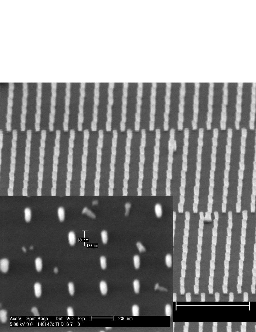
A nano-imprint assistant dry-etching procedure has been employed to fabricate Si NP on Silicon-on-Insulator (SOI) structure by Lamontagne et al sample . The pillars are separated by nm thick layer from the bulk Si substrate. The density of the NP in the nano-mask is cm-2. Fig. 1 shows Scanning Electron Microscope (SEM) pictures of the sample with various resolutions. The highly-ordered structure of the NP is well resolved. The following average dimensions of the NP have been observed: diameter of nm and height of nm. The inset in Fig. 3 shows the absolute reflection, , measurement in the vicinity of nm. According to this result, at nm, roughly four times lower than of a crystalline Si. Similar value, of decreased , was observed by G. R. Lin et al. Lin at an even broader spectrum on similar structures.
In the scope of the Drude model with neglected damping, the free carriers plasma refractive index is . Here and are the refractive indices of the bulk at the ground state and modified by the contribution from e-h plasma respectively. is the probing frequency while the plasma frequency denoted as . represents e-h plasma density, is the reduced effective mass of the e-h pair, and carry their usual meanings. Neglecting non-linear response, the relation between the change in the reflectivity and in the refractive index () at normal incidence can be expressed as: . Thus, allowing extraction of from the experimental data.
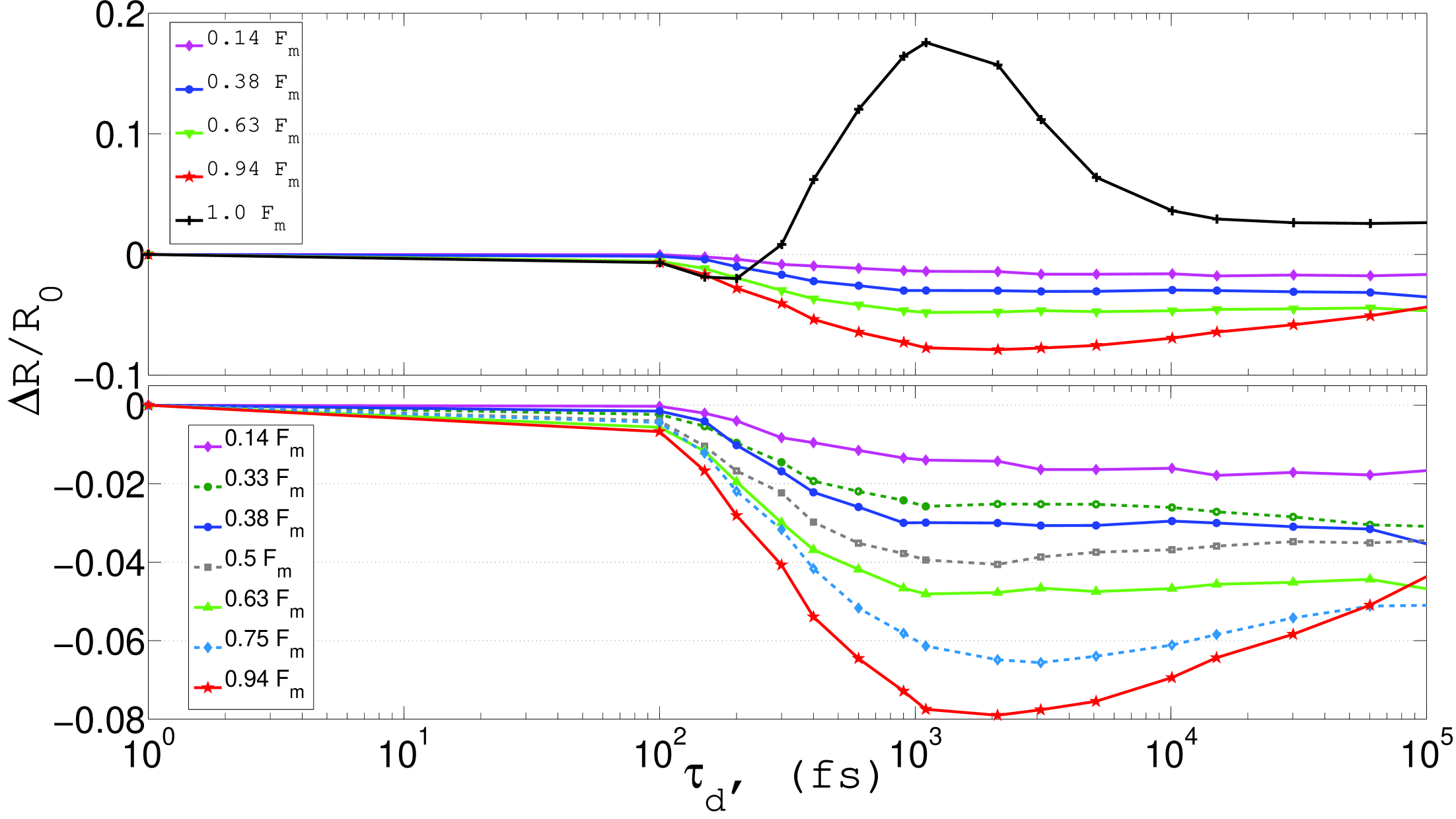
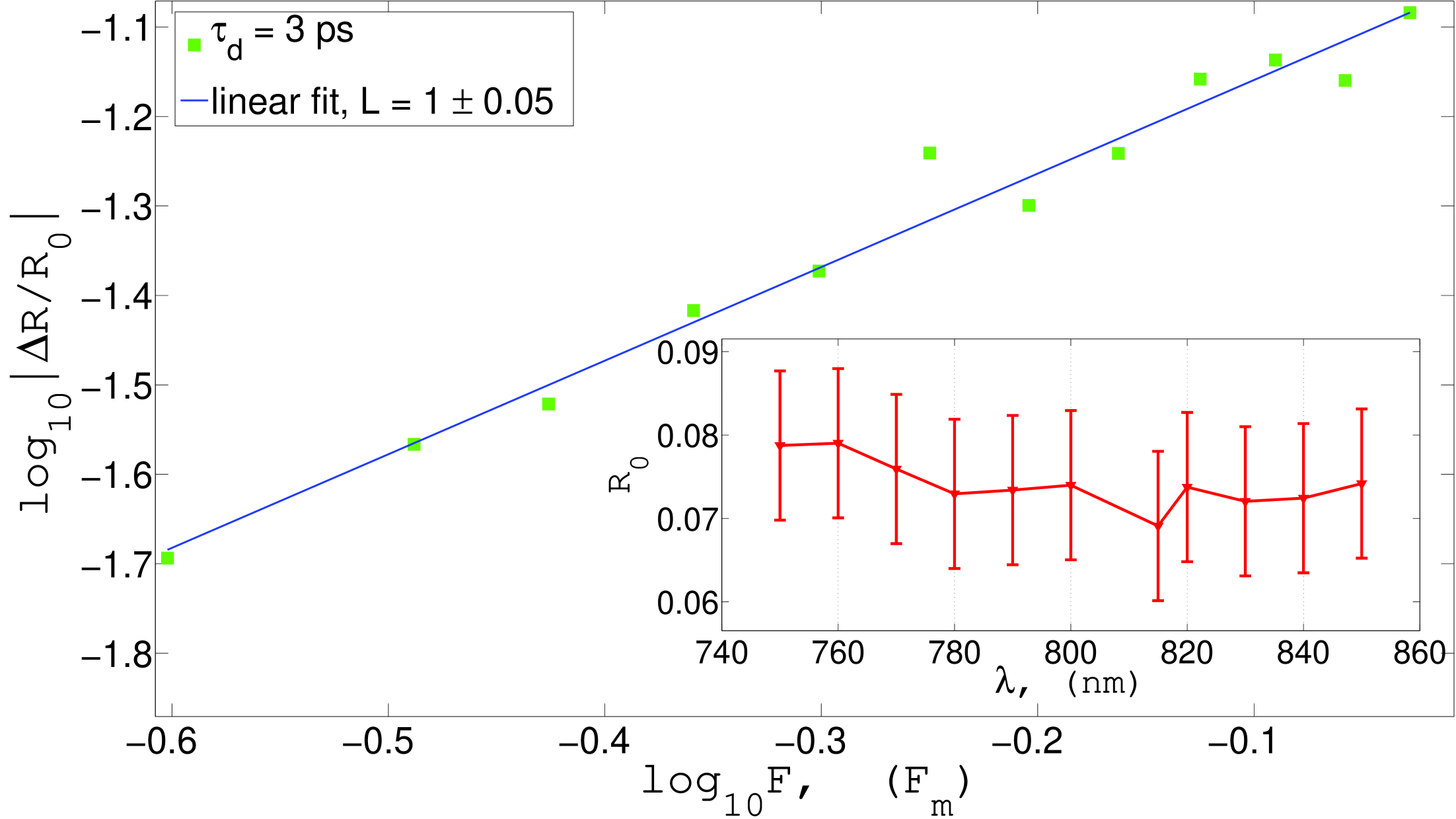
The time resolved versus the delay time, , recorded on the Si NP at different fluences in the range of (where mJ/cm2, is the threshold melting fluence of Si surface Sokolowski ) is shown in Fig. 2. The upper panel shows that at the melting fluence, , is predominantly positive. The initial reflectivity increase is attributed to the metal-like optical response contributed mainly by high-density e-h plasma which determines to be purely imaginary. After 1 ps decreases owing to carriers’ collision-enhanced e-h recombination process. The rest of the curves, recorded at the fluences below the melting point, present negative . Below the melting fluence a minimum of is reached after delay time of 1-2 ps. The largest change in the reflectivity, , is observed at . For comparison, similar measurements near the threshold fluence on a crystalline Si wafer provided negative of (not shown). Fig. 3 shows a supralinear plot of versus at ps. From the plot, the coefficient of non-linearity, , has been estimated as , demonstrating primary linear response of the pillars to the excitation.
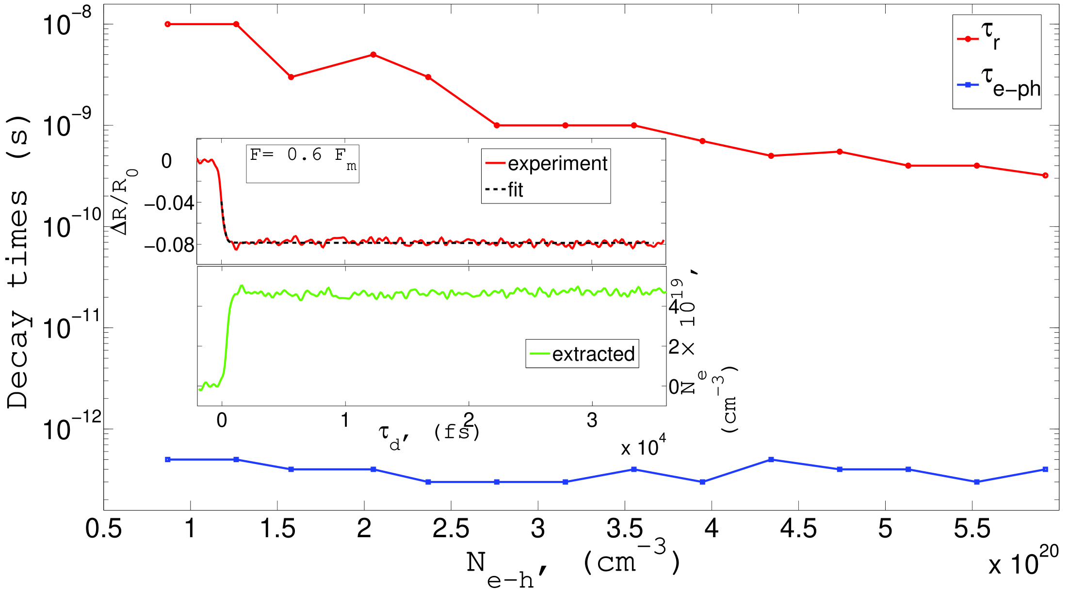
In order to analyze the fast and the slow electron dynamics, we have adopted the two-exponential model presented by Sabbah et al. Sabbah2002 (see Eq’s 6-8), here we note that for fitting we used , where is a fitting parameter. According to the model the fast component describes electron-phonon interaction and the slow represents e-h recombination. On the experimental curves, below the melting fluence, the fast component is responsible for the initial decrease in the reflectivity, , while the slow reflects its long recovery. The upper inset of Fig. 4 shows representative fitting of the model to the experimental at . This experimental data was taken with higher resolution than that presented in Fig. 2. Similar analysis has been done for the decay curves measured at different fluences and the decay constants have been extracted. Fig. 4 presents these constants as a function of the initial which has been estimated assuming linear absorption with the coefficient cm-1 and is taken from the inset of Fig. 3: , where is the photon excitation energy. The long decay time, , describes the e-h recombination time. It is found to depend strongly on the plasma density, decreasing from 10 ns down to 300 ps, at the density range of cm-3. The lower inset of Fig. 4 shows stability of the carriers population (after initial change) on the timescale of tens of picoseconds at a fluence of ( cm-3). The short decay, , is found to be independent of and estimated to be fs.
In conclusion, we have studied carriers dynamics in the excited crystalline Si NP. It is clearly shown that under strong diffusion suppression and at near submelting regime, the recombination time of the e-h plasma is much longer than reported for a bulk material: by UV excitation Tanaka and diffusion dominated behavior Shank . The thermalization time, however, remains unaffected. The initial drop of the reflectivity is up to 8% which is a few times higher than for the bulk silicon.
The authors appreciate the help of D C Sirica Ltd with the samples provided and thank E. Baskin for fruitful discussions during this work. We thank M. Y. Song for the SEM analysis. We acknowledge the financial support of AWM ”Science City” network and UK EPSRC.
References
- (1) B. E. Sernelius, Phys. Rev. B 40; S. Jallepalli, M. Rashed, W. K. Shih, C. M. Maziar, and A. F. Tasch, J. Appl. Phys. 81, 2250 (1997).
- (2) C. V. Shank, R. Yen and C. Hirlimann, Phys. Rev. Lett. 50, 454 (1983).
- (3) K. Sokolowski-Tinten and D. von der Linde, Phys. Rev. B 61, 2643 (2000).
- (4) A. Othonos J. Appl. Phys. 83, 1789 (1998).
- (5) Frederick C. K. Au, K. W. Wong, Y. H. Tang, Y. F. Zhang, I. Bello, and S. T. Lee, Appl. Phys. Lett. 75, 1700 (1999).
- (6) N. Koshida, ”Device Applications of Silicon Nanocrystals and Nanostructures”, Series: Nanostructure Science and Technology, Springer, 2009.
- (7) R. Buhleier, G. Lupke, G. Marowsky, Z. Gogolak, and J. Kuhl, Phys. Rev. B 50, 2425 (1994).
- (8) F. E. Doany and D. E. Grischkowsky, Appl. Phys. Lett. 52, 36 (1988); W. Kutt, A. Esser, K. Seibert, U. Lemmer, and H. Kurz, Proc. SPIE 1268, 154 (1990).
- (9) A. J. Sabbah and D. M. Riffe, J. Appl. Phys. 88, 6954 (2000).
- (10) A. Esser, W. Kutt, M. Strahnen, G. Maidhorn, and H. Kurz, Appl. Surf. Sci. 46, 446 (1990); F. E. Doany, D. E. Grischkowsky, and C. C. Chi, Appl. Phys. Lett. 50, 460 (1987).
- (11) T. Tanaka, A. Harata and T. Sawada, Appl. Phys. Lett. 82, 4033 (1997).
- (12) J. P. Woerdman Philips Res. Rep. 7, 12 (1971).
- (13) C. M. Li, T. Sjodin, and H. L. Dai, Phys. Rev. B 56, 15252 (1997).
- (14) A. Kaplan, M. Lenner, and R. E. Palmer, Phys. Rev. B 76, 073401 (2007).
- (15) B. Lamontagne et al, Department of Engineering Physics, Ecole Polytechnique, Montréal, QC H3T 1J4, Canada.
- (16) G. R. Lin, Y. C. Chang, E. S. Liu, H. C. Kuo and H. S. Lin, Appl. Phys. Lett. 90, 1819231 (2007).
- (17) A. J. Sabbah and D. M. Riffe, Phys. Rev. B 66, 165217 (2002).