Current-perpendicular-to-plane magnetoresistance of a domain wall confined in a nano-oxide-layer
Abstract
We theoretically study the current-perpendicular-to-plane magnetoresistance of a domain wall confined in a current-confined-path (CCP) structure made of a nano-oxide-layer (NOL). In order to calculate the MR ratio of the system, the continuity equations for charge and spin currents are numerically solved with the three-dimensional CCP geometry by use of finite element method. It is confirmed that the MR ratio is enhanced by the CCP structure, which is consistent with the experimental results.
pacs:
75.10.Jm, 75.50.Ee, 02.30.IkCurrent-perpendicular-to-plane giant magnetoresistance (CPP-GMR) has attracted much attention for its potential application as a read sensor for high-density magnetic recording. In order to realize a high-density magnetic recording, we need MR devices with high MR ratio and low resistance area product (RA). Although the RA value of a CPP-GMR system is much smaller than that of a tunneling magnetoresistance (TMR) system, the MR ratio of a conventional CPP-GMR system still remains a small value of a few %. Much effort has been devoted to increasing the MR ratio of the CPP-GMR system. One of the candidates for such a device is the CPP-GMR spin-valve with current-confined-paths made of a nano-oxide-layer (NOL) with a lot of small metallic channels fukuzawa04 ; fukuzawa05 . The MR ratio of 10.2% is obtained by the CPP spin-valve with non-magnetic Cu nanocontacts. This MR enhancement by the CCP structure was theoretically studied in detail in Refs. imamura07 ; smi08 .
Recently, Fuke et al. showed that such MR enhancement appears even in the system with ferromagnetic nanocontacts. They obtained the MR ratio of 7-10% by the CoFe nanocontacts in NOL with CCP structure fuke07 . It seems that this MR effect originates from the spin accumulation around the domain wall confined in the NOL.
In order to analyze this experimental result, we calculate the MR ratio of the CCP system with a domain wall. The MR ratio is determined from the distribution of the spin accumulation around the domain wall, which is obtained by solving the spin diffusion equation valet93 ; zlf with the use of finite element method ram-mohan ; ichimura07 .
Let us begin with a brief introduction to the theory of the spin diffusion equation zlf , which we solve to determine the MR ratio of the system. According to the Ref. zlf , the electric current and the spin current can be written as
| (1) | ||||
| (2) |
where we choose the unit such as the charge of an electron and the Bohr magneton are set to be 1: . Here we omit the term proportional to the derivative of the charge accumulation. The vectors denoted by the arrow represent those in real space and the bold font represent those in the spin space. is the electric field and is the spin accumulation. The conductivity and the diffusion constant are written in the spinor form as , , where the are the Pauli matrices. and are proportional to the spin polarization parameters and as and , where is the unit vector in the direction of the local magnetization.
In order to derive the equation to determine the spin accumulation , we eliminate the electric field from the equations (1) and (2) and obtain
| (3) |
For convenience we introduce an operator acting on the spin space as
| (4) |
where we write the components of the local magnetization as . With the use of this matrix , the expression of the spin current is simplified into
| (5) |
The continuity equation for the spin accumulation takes the form zlf
| (6) |
where is the coupling constant of the interaction between the spin accumulation and the local moment, and is the spin-flip relaxation time of the conduction electron. In order to obtain the solution for the stationary state, we set the left hand side of Eq. (6) to zero,
| (7) |
Introducing the matrix on the spin space as
| (8) |
we obtain the equation for the spin accumulation to be solved
| (9) |
The determination of the MR ratio of the system consists of the following three steps. First we determine the charge current density from the continuity equation . Next we solve the Eq. (9) for a given local magnetization in the domain wall and determine the spin accumulation . Finally we determine the voltage drop of the system by integrating the electric field . Since we apply the constant electric current density, the voltage drop is proportional to the total resistance, from which we obtain the MR ratio of the system.

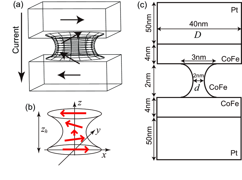
Now we move onto the analysis of the MR ratio of the CCP spin-valve with a domain wall. The system we consider is schematically shown in Fig. 1 (a). A domain wall is confined in a nanocontact, which is sandwiched between pinned layer and free layer. We adopt Bloch domain wall as a magnetic structure in the nanocontact. The local magnetization is given by , where is the thickness of the nanocontact (=2nm) and is the height from the bottom of the nanocontact as is shown in Fig. 1 (b).
The cross-sectional view of the system is shown in Fig. 1 (c). The curve of the contact region is modeled by the half ellipse, which is tangent to the ferromagnetic layer. The length of the major axis of the ellipse, which is the same as the thickness of the contact, is taken to be 2 nm. The length of the semi-minor axis of the ellipse is 1 nm. The pinned and free layers are assumed to be 40nm40nm4nm rectangles. We also consider the Pt capping layer with the thickness 50nm. We set the value of the resistivity of Pt layer as large as so that the total RA without CCP structure is which is the value reported in the experiments fukuzawa04 ; fukuzawa05 .
The spin accumulation is determined by numerically solving Eq. (9) by use of the finite element method ram-mohan , ichimura07 . The system is divided into hexahedral elements and the total number of elements is of the order of 104. We assume that the free and pinned layers and the nanocontact are all made of CoFe. We use material parameters for the conventional CPP-GMR spin-valve system; , , , , , where denotes the spin diffusion length. Especially we adopt the value of resistivity of CoFe in the contact region as 1m, which is the value reported in the experiments fukuzawa04 ; fukuzawa05 . This enhancement of the resistivity in the contact region is due to the decrease of the purity of CoFe in the oxidation process. The diffusion constant and the relaxation time are determined by the relation and , where we set the density of states at the Fermi level as .
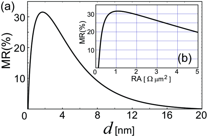
In order to examine the MR enhancement effect by the CCP structure, we first vary the contact diameter with the fixed size of the electrode . The dependence of MR on is shown in Fig. 2 (a). The MR enhancement effect by the CCP structure is confirmed by the simulation as is shown in the figure, where the MR ratio increases with decreasing the contact diameter from nm to nm. If we completely confine the contact region , no electric current can flow and MR ratio becomes zero. This implies the existence of the contact diameter which maximize the MR ratio. Actually we observe sharp peak around 2 nm in Fig. 2 (a). In practice, in the region where the contact diameter is less than the order of 1 nm, the diffusion equation loses its validity and the quantum mechanical approach is necessary. In Fig. 2 (b) we replot the MR ratio against the resistance area product RA. The value of RA without CCP structure is set at . It is observed that if we decrease the contact diameter, the MR increases with increasing RA and takes its maximum value around RA.

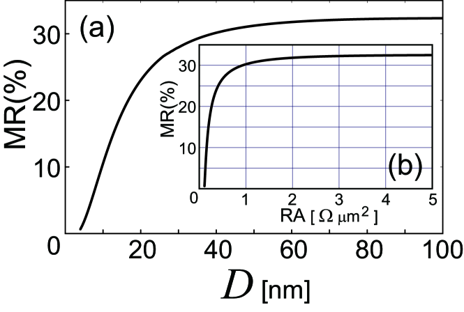
Next we vary the size of the electrode with the fixed contact diameter =2nm. Since enlarging the size of the electrode corresponds to increasing the distance between nanocontacts in the NOL, the effect of changing the density of nanocontacts can be realized in our simulation by varying the size of the electrode. The dependence of MR on is shown in Fig. 3 (a). The MR is a monotonic increase function of and is saturated around 50nm as is shown in the figure. This means that the MR monotonically increases with decreasing the density of nanocontacts and is saturated at a certain value of density. In Fig. 3 (b) we replot the MR ratio against the resistance area product RA. Since RA increases with decreasing the density of nanocontacts, we observe a monotonic increasing dependence of MR on RA unlike the case with varying the contact radius in Fig. 2 (b) where MR has maximum value at RA. Although the MR shows monotonic increasment with RA, it is saturated around RA.

In summary, we studied the current-perpendicular-to-plane magnetoresistance of a domain wall confined in a CCP structure made of an NOL. We solved the continuity equations for charge and spin currents with the three-dimensional CCP geometry by use of finite element method. We have confirmed that the MR enhancement effect by the CCP structure from the calculation of MR with varying the contact radius and the electrode size . We observed that the MR is maximized at 2nm. In our simulation with varying the electrode size , it is observed that the MR increases with decreasing the density of nanocontact and is saturated at a certain value of density.
Acknowledgement
The authors thank M. Sahashi, M. Doi, H. Iwasaki, M. Takagishi, Y. Rikitake and K. Seki for valuable discussions. The work has been supported by The New Energy and Industrial Technology Development Organization (NEDO).
References
- (1) H. Fukuzawa, H. Yuasa, S. Hashimoto, K. Koi, H. Iwasaki, M. Takagishi, Y. Tanaka, and M. Sahashi, IEEE Trans. Magn. Mater. 40, 2236 (2004).
- (2) H. Fukuzawa, H. Yuasa, S. Hashimoto, H. Iwasaki, Y. Tanaka, Appl. Phys. Lett. 87, 082507 (2005).
- (3) H. Imamura, PHYSICA STATUS SOLIDI B-BASIC SOLID STATE PHYSICS 244, 4394 (2007).
- (4) J. Sato, K. Matsushita and H. Imamura, preprint: arXiv:0806.3314
- (5) H. N. Fuke and S. Hashimoto, M. Takagishi, H. Iwasaki, S. Kawasaki, K. Miyake, and M. Sahashi, IEEE Trans. Magn. 43, 2848 (2007).
- (6) T. Valet and A. Fert, Phys. Rev. B 48, 7099 (1993).
- (7) S. Zhang, P.M.Levy and A. Fert, Phys. Rev. Lett. 88, 236601 (2002).
- (8) L. Ramdas Ram-Mohan, “Finite element and Boundary Element Applications in Quantum Mechanics”, Oxfort University Press(2002)
- (9) M. Ichimura, J. Ieda, H. Imamura, S. Takahashi and S. Maekawa, Journal of Magnetism and Magnetic Materials, Volume 310, Issue 2, Part 3, March 2007, Pages 2055-2057