Correlations between the morphology and the electronic structure at the surface of thin film manganites, investigated with STM.
Abstract
Thin-film colossal magnetoresistance manganites such as La0.67Ca0.33MnO3 (LCMO) have now been intensely studied for more than a decade, but the issue of possible nanoscale electronic phase separation is not fully solved. Scanning Tunneling Microscopy / Spectroscopy (STS) has been pivotal in studying phase separation, but is hindered by being surface- rather than bulk-sensitive. For our sputtered LCMO films the data indicates a strong correlation between surface morphology and signatures of phase separation; rough films show phase separation while atomically flat films are electronically homogeneous but have a more or less inactive surface layer. Regardless of surface morphology, the film bulk is electronically and magnetically active. Many of the reported conclusions about electronic inhomogeneities measured by STS have been confused by this issue. We study both strained and unstrained films and find no correlation between substrate-induced strain and either electronic phase separation or dead layers.
pacs:
75.47.Lx,73.25.+i,73.50.-hI Introduction
Hole-doped manganites, such as La0.67Ca0.33MnO3, have been widely studied, not only because they exhibit colossal magnetoresistance (CMR), but also because of interest in the coupled metal-insulator (-) and ferromagnetic-paramagnetic transition they demonstrate. One unanswered question is how electronic phase separation (PS) occurs, that is its spatial structure as function of temperature and magnetic field, and how that connects to the CMR effect observed in transport measurements. Local-probe techniques, such as scanning tunneling microscopy (STM) and magnetic force microscopy, would seem to be ideal tools to explore this, and a number of groups have studied thin-film manganites using these methods.Fäth et al. (1999); Becker et al. (2002); Chen et al. (2003); Seiro et al. (2008); Biswas et al. (2001); Zhang et al. (2002) Some reports find PS on the scale of many nanometers up to micrometers. Because of the electrostatic energy cost of domains on the order of micrometers, phase separation should be limited to nanometers, unless large disorder is present,Moreo et al. (2000); Dagotto et al. (2008) suggesting that disorder must play a role in such large-scale PS. However, extensive investigations, both experimentally and theoretically, also indicate that manganite surface properties can differ from bulk properties.Borges et al. (2001); Abad et al. (2005); Yao et al. (2006); Valencia et al. (2007); Choi et al. (1999); Simon et al. (2004); Estradé et al. (2007); Calderón et al. (1999); Filippetti and Pickett (2000); Zenia et al. (2005) This is of obvious relevance, since techniques such as scanning tunneling microscopy (STM) and spectroscopy (STS) are inherently surface-sensitive. Nevertheless, from STM and STS measurements of thin-film manganites, evidence of half-metallicity,Wei et al. (1997) polarons,Wei et al. (1997); Seiro et al. (2008) and pseudo-gaps,Mitra et al. (2005) have all been claimed, while spatial electronic phase separation has been mapped as a function of both applied magnetic field, Fäth et al. (1999); Chen et al. (2003) and temperature.Becker et al. (2002) These surface measurements are purported to represent bulk properties, but we want to reconsider this issue, which has been further clouded because STM/STS measurements have been made on a variety of systems. It should be realized that spatial inhomogeneities can be significantly different for wide bandwidth systems such as La1-xSrxMnO or narrow bandwidth systems such as La1-xCaxMnO3; or for differing strain states such as fully strained versus (partially) relaxed. We present an STM/STS study confined to thin-film La0.67Ca0.33MnO3 (LCMO), that is, at optimal doping and therefore far from the regime where the material might become intrinsically insulating. We vary thickness, strain, and surface morphology. Strained films are grown on SrTiO3 and unstrained films are grown on NdGaO3. Film thicknesses range from 10 to 180 nm. We expect the thinner films, on the order of 10 to 25 nm, to be coherently strained and thicker films, of 100 nm and more, to be strain-relaxed. We found that film surface morphology varied with film thickness. Then we compare our surface-sensitive STM and STS measurements to bulk-sensitive measurements of these same films.
II Experiment
II.1 Growth and Characterization
Thin films of LCMO with thicknesses between 10 nm and 180 nm were grown on single crystal substrates of SrTiO3(001) and NdGaO3(001). All films were grown using dc sputtering from stoichiometric targets in 3 mbar of pure oxygen. Film thickness was determined by sputtering time and verified with X-ray reflectivity measurements of selected films (see below for details). Various substrate temperatures were used during film growth, all between 780 ∘C and 840 ∘C. Some films were annealed in-situ, immediately after sputtering. Others were annealed ex-situ in flowing pure oxygen at atmospheric pressure.
Surface morphology was verified with tapping-mode atomic force microscopy.
Resistances versus temperature (-) transport measurements were made using four in-line probes attached to the film with either silver paste or indium or using structured bridges. For unstructured measurements, as the probes were of variable size and with variable distance, only resistance and not resistivity was obtained. Nevertheless, normalized - curves are sufficient to observe the - transition and CMR and to characterize film quality. X-ray diffraction (XRD) measurements were made with a Siemens D5005 using a Cu K source. Film thicknesses were determined using low-angle XRD, while film quality was verified with Laue oscillation measurements. X-ray photoemission spectroscopy (XPS) measurements were made using a Mg anode (1253.6eV) and hemispherical analyzer in a UHV measurement chamber with base pressure on the order of mbar. Samples were either baked overnight in a load-lock at approximately 100∘ C to desorb surface contaminants, or brought into the measurement chamber rapidly to retain any contamination present on the sample surface. Some films were plasma etched using both O2 and Ar at a calibrated etch rate of 1 nm/minute. This combination has been shown to etch STO without depleting its oxygen and rendering it metallic.Beekman et al. (2007)
II.2 STM
STM measurements were made under various conditions, ultra high vacuum (UHV), flowing helium gas, and ambient. All of our STM heads were built in-house and use a course approach based upon the Pan design.Wittneven et al. (1997) Both mechanically cut PtIr (90%:10%) and electrochemically etched Pt wires were used as STM tips. The UHV STM chamber has a base pressure of mbar, with the capability to vary the sample temperature between 300 mK and 180K and the possibility to apply magnetic fields up to 8 T. Samples were brought into the UHV chamber after being pumped overnight in a load-lock.
Other STM measurements were conducted in helium boil-off gas within a variable temperature insert (VTI) mounted through the bore of a 12 T magnet. Using resistance heating, the sample temperature can be varied between 4.2 and 340 K. Once inserted into the cryostat, samples were held between 300 K and 340 K while being flushed with dry helium gas to effect desorption of contaminants. To minimize the sample cryopumping while at low temperatures, samples were kept warmer than the surrounding VTI. Ambient STM measurements were made using the same STM as used for helium gas measurements, but without inserting the STM into the VTI.
Conductivity maps were measured using a digital lock-in amplifier. While scanning topography, the STM bias voltage () was modulated with an ac voltage () from an oscillator built into the lock-in amplifier. The ac modulation was limited in amplitude to a few percent of the bias voltage, and at a frequency higher than the feedback bandwidth (on the order of 1 kHz). Conductivity was computed by the lock-in using output from the STM current-to-voltage amplifier.
Current-voltage curves (-) were measured using a fixed tunneling gap method. This begins with the STM in tunneling at particular bias () and current () set-points and with the feedback engaged. The STM feedback is then disengaged, freezing the tip-sample distance while the bias voltage is swept through the desired voltage range. Simultaneously, both the applied bias voltage and the measured tunneling current were recorded. Up to 500 curves were taken and averaged for each - curve. Measured - curves were numerically differentiated after averaging. Resulting d/d spectra were used as a proxy for sample density of states (DOS).
III Results
III.1 Growth and Characterization
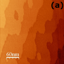
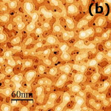
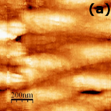
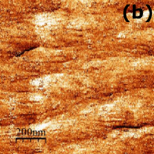
With increasing film thickness, we observe that, for films grown on both NGO and STO, the surface changes from flat terraces with a unit-cell step height, 0.4 nm, to a rougher morphology, 10 to 20 nm peak-to-peak, with no indication of terraces. We also observe that terraced films can be further divided into those with long narrow terraces and those exhibiting 2-D island growth. Typical examples of terraced and 2-D island growth morphology are shown in Figure 1. Both of these films are 10 nm thick, were grown on STO substrates, and measured with an STM in ambient conditions. Although for films grown on STO with thicknesses between 10 and 50 nm both morphologies were found, the predominant morphology was terraced. Since growth conditions were nominally the same, we attribute the occasional appearance of island growth to the varying quality of the commercial substrates. However, other researchers have noted a change from terrace growth to 2-D island growth for LCMO grown on low miscut angle STO as films thickness is increased above 30 nm.Sanchez et al. (2006) For our thicker films on STO, those about 100 nm and thicker, the surface morphology becomes rough. Terraced and 2-D island growth was also seen for films grown on NGO and are similar in appearance to the STO films shown in Figure 1. However, for films grown on NGO, a correlation between film thickness and surface morphology is apparent. The thinnest films, around 10 nm thick, were almost exclusively terraced. Medium thickness films, around 25 nm thick, generally exhibited 2-D island growth. Thicker films, those thicker than 50 nm, were usually rough.
Transport measurements were made on some of our films. Shown in Figure 2 are example - measurements for flat LCMO films grown on STO and NGO. From such curves we can extract the peak temperature (). These curves were normalized to the zero-field peak resistance. The peak temperatures are typical for strained films grown on STO ( K) and unstrained films grown on NGO ( K), though does vary a little with film thickness. Also shown for the STO film is an - measurement in magnetic field that confirms this film to be magnetoresistive. Similar measurements were made of other films, both flat and rough. We can conclude that the film bulk of both our flat and rough films have an - transition and are magnetoresistive.
 |
 |

XPS measurements were made of a subset of films to confirm the presence of lanthanum, calcium, manganese, and oxygen and to verify the absence of other, contaminating elements at the film surface. Except for carbon, no evidence of contamination was observed. Since carbon contamination is ubiquitous, and as sample cleaning was limited to moderate in-situ heating, the presence of carbon is not unexpected, and does not necessarily indicate a poor quality film.Beyreuther et al. (2006)
III.2 STM
STM and STS measurements were taken of LCMO films with various thicknesses grown on STO and NGO substrates. Both flat films, those with terraced or 2-D island growth, and rough films, those with rounded morphology and no discernable unit-cell steps, were measured.
III.2.1 Rough Morphology
 |
 |
 |
 |
 |
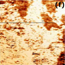 |
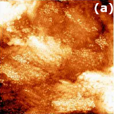
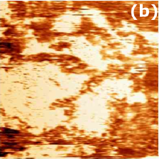
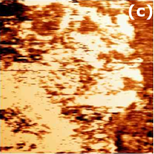
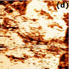
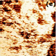
Thicker LCMO films grown on either STO or NGO were rough and show evidence of phase separation and an electronically and magnetically active surface layer. Figure 3 (a) displays topography for a 100 nm thick film grown on Nb-doped STO. The film surface is rough, with peak-to-peak height variations of 20 nm. Also seen in Figure 3 is a sequence of conductivity maps covering the same area as shown in Figure 3 (a), but for different applied magnetic fields. As the applied field is increased, the metallic (dark) area increases and the insulating (light) area decreases. Note that some insulating regions do increase in size at higher fields. Nevertheless, the predominant trend is an overall increase in metallic regions. There is some correlation between surface morphology and conductivity, though not as significantly as seen in other films (see below). Although these conductivity maps were measured at 50 K, well below the - transition temperature, electronic inhomogeneities are still present, even with a 7 Tesla applied magnetic field. Similar results were obtained by Fäth et al,Fäth et al. (1999) on a similarly rough LCMO film, although their film was grown with a YBa2Cu3O7 layer between the LCMO film and the STO substrate.
 |
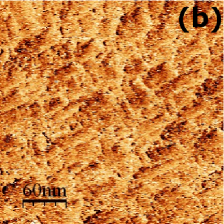 |

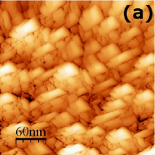
Rough films grown on NGO were also inhomogeneous. This is confirmed by both conductivity maps and d/d spectra. An example of topography and conductivity map of a rough LCMO film on NGO is shown in Figure 4. This film is 50 nm thick, with rough topography (10 nm peak-to-peak), and, as with rough samples on STO, with an inhomogeneous conductivity map (darker regions are more metallic, lighter regions are more insulating). Note that there is significant correlation between the conductivity map and topography. This is not because of feedback-error since the forward and reverse scans of the conductivity map are very similar, but rather reflect properties of the surface. This particular measurement was made at 280 K, just above , where phase separation would be expected. However, other conductivity maps of this film recorded above and below are similarly inhomogeneous. Unfortunately, due to the difficulty of calibrating conductivity maps measured with a lock-in amplifier, only qualitative information can be gleaned from such measurements. To provide quantitative information, d/d spectra were also taken of this film. Spectra taken at different locations indicate the presence of both metallic and insulating regions, confirming the electronic inhomogeneity seen in conductivity maps. Examples of d/d spectra are shown in Figure 5. Both curves were measured on the same film as shown in Figure 4 but at 299 K, significantly above . The zero bias conductivity at this temperature varies by an order of magnitude, from to siemens. These curves demonstrate that even well above , rough films are inhomogeneous. Other d/d spectra measured in and well below the - transition indicate electronic inhomogeneity. Measurements of other rough films confirm these results.
III.2.2 Smooth Morphology
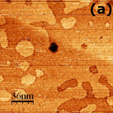
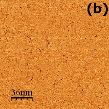
Thinner films grown on either NGO or STO were atomically smooth and electronically homogeneous with electronically and magnetically inactive surface layers. A typical example of topography and conductivity for a 10 nm thick terraced STO film is shown in Figure 6. This measurement was made in zero magnetic field at 150 K, close to the film’s . For a first-order phase transition, we expect to see inhomogeneities at temperatures close to . However, we saw no evidence of phase separation at this temperature or at any other. What detail there is in this conductivity map is at terrace edges and defects. We attribute this to feedback error, the increased or decreased conductivity resulting from the tip coming closer to or going further away from the surface. Varying the STM bias voltage, current set point, or ac-modulation voltage did not change this result. Conductivity maps taken at temperatures above and below the - transition were similarly featureless. Conductivity maps were also made of other flat LCMO films on STO. All were similarly homogeneous, regardless of the temperature. Similar results were seen for smooth films grown on NGO.
 |
 |

/ spectra were taken of flat films grown on STO and NGO. These spectra show small variations with temperature, but no consistent trend in zero-bias conductivity. They also indicate that our flat films were spatially homogeneous. An example of d/d spectra measured on a terraced STO film is shown in the left-hand column of Figure 7. For this film, 52 nm thick LCMO on STO, 155 K. Shown in the figure are spectra from above, below, and at . At each temperature are plotted the spectra calculated from two (or three) - measurements at bias set-points 0.25 (green), 0.5 (red), and 1.0 V (black), but all with =0.5 nA. In these - measurements, the bias was swept from the to . The spectra measured at and were linearly scaled by a procedure explained in the Appendix. The need to measure at different set-points is made clear by looking at the data for . Between 0.3 V, the spectra are very noisy because between these voltages the resulting current is below the system noise floor. Reducing while maintaining fixed increases the set-point conductance linearly, but, because of the non-linear nature of the tunneling gap, the conductance at low voltages has increased much more. This point is expanded upon in the Appendix. Because of this increase in conductance, and as can be seen at all three temperatures, more of the narrow spectra are above the noise floor. From this it must be concluded that there is not a gap, but only a depletion of the DOS at zero bias. At other temperatures, varying between 170 K and 80 K, d/d spectra of this film also show no significant variation. Other smooth LCMO films grown on STO and NGO were measured and also demonstrate no consistent variation in d/d spectra with temperature.
Shown in the right-hand column of Figure 7 are the d/d spectra from the left-hand column at =0.5 V , but normalized by dividing by . Normalizing in this way attempts to extract the DOS from the d/d spectra, by canceling the effect of the tunneling gap.Stroscio and Feenstra (1993) With this normalization procedure, earlier studies claimed to observe both polaron peaksWei et al. (1997); Seiro et al. (2008) and half-metallicityWei et al. (1997) in manganite films. We measured d/d spectra from many flat films grown on both STO and NGO and normalized these spectra with this method. Some of our data did suggest polaron peaks, but these polaron peaks do not appear on all films measured, even if grown under identical process conditions. When polaron peaks were evident, the peak-to-peak gap varied little with temperature, and no trend, such as seen in Ref. Seiro et al. (2008) was apparent. We applied this normalization procedure to d/d spectra taken at larger voltage setpoints ( volt), but found that, in the range of bias voltages where we would expect to see polaron peaks, the signal-to-noise ratio was too low.

We also measured atomically smooth films in an applied magnetic field. Shown in Figure 8 are d/d spectra measured on a smooth 26 nm thick film grown on NGO in zero field and in a 5 Tesla field. This data was taken at T=265 K, close to the - transition of this film (=260 K). These spectra are very similar to each other and to other spectra taken on other parts of the film, and also to spectra taken at other temperatures. Any differences are attributable to experimental error and show no correlation with either temperature or magnetic field. As we expect a large negative magnetoresistance in the vicinity of the - transition, this result suggests that the film surface is magnetically inactive. Transport measurements (shown in Figure 2) verify that the bulk of this film does go through a - transition. Again, this suggests the film surface is inactive. Other smooth films on NGO and STO were similarly unresponsive to magnetic fields.
III.2.3 Annealing and Etching
We attempted to remove the electronically inactive layer observed on flat films using a plasma etcher. Similarly to Hudson et al,Hudson et al. (2001) we found that once etched, the film surface became electronically active, but that the results were inconsistent from sample to sample. Etching 1 or 2 nm did modify the d/d spectra, but did not result in the appearance of metallic spectra (meaning a significant increase in zero-bias conductivity). After etching about 3 nm, we were able to measured some metallic d/d spectra. On these films we typically measured a number of metallic d/d spectra at temperatures somewhat below . The typical temperature window for this metallic phase was between 5 and 15 K wide. However, upon cooling to lower temperatures, the metallic phase was no longer evident, and instead of staying metallic, the d/d spectra became insulating and similar to those seen above the transition. Atomic force microscopy images of etched films show that etching initially followed the existing topography, leaving terraces with an appearance similar to as-grown. Further etching (3 nm or more) rounded off terrace edges, roughening the film, and giving it the appearance of an as-grown rough film. Etching did not produce spectra consistent with the - transition seen in transport measurements of these films, and it is unlikely that our STS data are representative of film-bulk behavior. The results also indicate that etching does something else than simply removing an inactive surface layer from the active bulk material.
One possible explanation for the inactive surface layer is oxygen depletion. We attempted to reoxidize films by annealing them in an oxygen-rich atmosphere. One sample was annealed in-situ in 1000 mbar of oxygen at 650∘C for 30 minutes. This sample proved to be electronically inactive. We also tried to eliminate possible causes of oxygen depletion. Although our films were typically grown in 3 mbar of oxygen, our usual process recipe called for evacuating the process chamber immediately after sputtering was complete. Thus while cooling, the film would be exposed a vacuum on the order of mbar. Beyreuther et al found below-stoichiometry oxygen in manganite films exposed to UHV at elevated temperatures (470-670∘C),Beyreuther et al. (2006) and so we attempted to minimize film deoxidization by maintaining 3 mbar of oxygen during cooling. The resulting film was still electronically inactive. Following their recipe for film reoxidization, we annealed a sample at 470∘C in flowing oxygen for 3 hours. The resulting film was electronically active, but inhomogeneous. Ambient STM topography and conductivity map shown in Figure 9. The film was roughened by the annealing. In contrast, before annealing, the film exhibited 2-D island growth with a homogeneous conductivity map.
 |
 |
IV Discussion
We were able measure electronically active surface layers on rough films. Other researchers have found similar results using STM/STS on rough films. The surface of our flat, smooth films are electronically and magnetically inactive. However, using methods other than STM/STS, researchers have also observed inactive surface layers on manganites, and a number of explanations for the origin of this layer have been put forth. Measurements have detected both oxygen depletion and dopant enrichment at the surface, both of which would change its electronic structure. Others have proposed surface electronic reconstruction driven by symmetry breaking at the crystal surface. We now discuss these various points in some detail.
IV.1 Other STM Results
IV.1.1 Rough Films
In agreement with our data, other researchers have measured inhomogeneities on rough films. Becker et al measured an LCMO film grown on MgO and found it to be electronically inhomogeneous.Becker et al. (2002) Their film was 200 nm thick, with a rough, grain-like surface morphology. Fäth et al detected inhomogeneities on a rough (maximum 20nm peak-to-peak roughness) LCMO film on STO, and measured an increase in metallicity with increased magnetic field, as would be expected of a CMR material.Fäth et al. (1999) Chen et al also detected electronic inhomogeneities on an LCMO film grown on STO.Chen et al. (2003) Their film was 300 nm thick with peak-to-peak height variation of 7 nm over 50 nm lateral distance, with no evidence of terraces or unit-cell steps.
IV.1.2 Atomically Flat Films
Although a number of researchers reported electronically active surface layers on flat LCMO films using STM/STS, taken collectively, no clear picture emerges. Seiro et al published STS measurements of an LCMO film on STO.Seiro et al. (2008) STM topography indicated a terraced surface, and STS measurements showed the film to be spatially electronically homogeneous. They observe conductance peaks in their normalized d/d spectra, and claim these peaks to be the signature of polarons, with half the peak-to-peak distance representing the polaron binding energy. They found this binding energy varied with temperature, but narrowed in the region of , exactly where their transport measurements show the film to have its highest resistivity. Other groups also measured flat, but electronically active films. Both Biswas et alBiswas et al. (1999) and Mitra et alMitra et al. (2005) measured atomically flat LCMO films and observe that, in the vicinity of , a gap in the d/d spectra opens, corresponding to the peak resistivity of transport measurements. Conductivity maps measured by Mitra et al show their film to be electronically homogeneous, and they attribute this to their film being grown on NGO and therefore being unstrained. However, Biswas et al measured strained LCMO grown on LAO and make no mention of electronic inhomogenities. Both Seiro et alSeiro et al. (2008) and Mitra et alMitra et al. (2005); Paranjape et al. (2003) appear to present data taken from only one sample. We found inconsistencies between our films grown under nominally identical process conditions, and found our conclusions to be more robust when drawn from a number of samples. Furthermore, both groups present example - curves that appear to be measured at different voltage set points. Considering the difficulty of separating sample DOS from the tunneling barrier,Ukraintsev (1995); Koslowski et al. (2007) we would not want to draw conclusions from such a procedure and prefer to compare data taken at a single set-point, eliminating one source of uncertainty.
Other than our results presented here, only one other group has presented STM/STS data showing conductivity maps of both flat and rough films. Moshnyaga et al measured LCMO films on MgO at 115 K, significantly below the film - transition temperature.Moshnyaga et al. (2006) They found their flat film to be electronically homogeneous, while their rough film was inhomogeneous. Magnetization measurements indicate the flat film’s saturation magnetization was slightly lower than that of the rough film. For a fairly thick film (80 nm), a slightly reduced saturation magnetization would be consistent with a thin, magnetically-dead surface layer. Unfortunately, these researchers only measured conductivity maps at one temperature and without an applied magnetic field.
IV.2 Causes of the Inactive Layer
Because the STM tunneling current decreases exponentially with tunneling distance, Stroscio and Feenstra (1993) only the topmost conducting unit cell of the manganite will directly contribute to the d/d spectra. If the surface unit cell is electronically representative of the film bulk electronic structure, then the d/d spectra will be a measure of film bulk properties. However, if the surface unit-cell is not electronically representative of the film bulk but still conducting, then the d/d spectra will only represent surface layer properties. The film surface may differ electronically form the film bulk because it is chemically different : depleted or enriched in oxygen or dopants, or because the film crystal structure is necessarily truncated by the film surface.
IV.2.1 Dopant Enrichment and Depletion
Some studies have found evidence that LCMO films are not chemically homogeneous. Simon et al measured the chemical profile of a LCMO/STO/LCMO trilayer grown on an STO substrate. Simon et al. (2004) Using energy-loss spectroscopic profiling, they detected enhanced Ca doping at the surface of the first LCMO layer. They attributed this to a La-rich layer that forms adjacent to the STO substrate as film growth initiates. As there is lattice mismatch between LCMO and STO, at the film-substrate interface the film will be under tensile strain, favoring substitution of La2+, the slightly larger ion (1.36Å), for Ca3+, the slightly smaller ion (1.34Å). Because a fixed ratio of LCMO precursors is sputtered onto the substrate, a Ca-rich layer must form on top of the La-rich layer. Once formed, the Ca-rich layer floats on the surface while the film grows beneath it. However, this explanation may not hold; Choi et al Choi et al. (1999) measured a Ca-enriched surface layer on an LCMO film on LAO (where no tensile strain occurs) using angle-resolved XPS. They found a best-fit model of their data to be a single Ca-enriched layer at the film surface (60% Ca doping), significantly above the nominal 35% film doping. They hypothesize that this enriched layer was caused by a large heat of segregation driving Ca towards the surface. Estradé et al measured the chemical composition of LCMO films grown on both (001) and (110) oriented STO substrates with electron energy-loss spectroscopy. Estradé et al. (2008)They found differences between the surface and bulk concentrations only for the (001) orientation, although both orientations yield the same strain. Important for our purpose is that the segregation they found is only small. Although we have not studied our film’s surface chemistry, we find the same inactive layer on both strained flat films on STO and unstrained flat films on NGO, suggesting that, if there is any chemical stratification, substrate-induced strain is not the cause.
IV.2.2 Oxygen Depletion
Oxygen depletion can also shift the Mn valence. In some studies the surface Mn valence was measured directly and conclusions were drawn on surface oxygen depletion. Using XPS, Beyreuther et al measured exchange splitting of the Mn 3s core-level peak in LCMO on STO.Beyreuther et al. (2006) From this data they could infer the Mn valence in the top 3 nm of the film. For as-grown films, the Mn valence was +3.3, the expected bulk film value, but for films subsequently exposed to UHV at elevated temperatures, the Mn valence shifted towards +2. However, they found that the surface Mn valence could be restored to bulk value by reoxidizing the film in oxygen at elevated temperatures (470∘C). From this they conclude that the shifts in Mn valence were driven by oxygen depletion and enrichment. Other research has demonstrated that exposure to only moderate temperatures (80∘C) in air is required to reoxidize LCMO films,Dörr et al. (2000) and this suggests that an oxygen-poor atmosphere—such as helium gas—at similar temperatures could lead to oxygen depletion. However, many of our flat and rough films were measured in ambient before exposure to an oxygen-poor environment, and we could detect no difference between these measurements and subsequent measurements made in helium gas or UHV. Because we do not measure our films in-situ, it is possible that exposure to ambient conditions could degrade the surface in some way. This possibility has been investigated by other researchers. Valencia et al measured LCMO films grown on LAO using x-ray absorption spectroscopy (XAS). Valencia et al. (2006) For as-grown films, they measured spectra congruent with the expected Mn3+/Mn4+ ratio, but once the film had been exposed to air, they also detected the signature of Mn2+ ions. They propose the CO present in air as a reducing agent that attacks the unstable Mn3+ and Mn4+ ions. However, as they note, on films exposed to air for less than 2 days, they could not detect Mn2+ ions. Some of our films were measured after less than an hour of exposure to air, and we saw no difference between these films and those exposed to air for significantly longer. If the surface of our as-grown films is oxygen depleted, then this oxygen depletion seems likely to occur during growth or while cooling from the film-growth temperature.
IV.2.3 Symmetry Breaking
Theoretical modeling of doped manganites has indicated non bulk-like properties at the surface. Calculations by Calderon et al for the MnO2-terminated surface of La1-xAxMnO3 with , suggest that truncation of the crystal by the surface leads to charge transfer from the bulk to the surface Mn layer.Calderón et al. (1999) This charge transfer will create a Mn3+ ion-only layer, suppressing the double exchange interaction, and leading to an anti-ferromagnetic (AFM) coupling within this layer. These calculations also demonstrate that transport perpendicular to the surface layer is significantly reduced for an AFM-coupled surface when compared to a ferromagnetically-coupled surface. Filippetti et al considered ferromagnetic (FM) versus AFM coupling between the surface and immediate subsurface layer of MnO2-terminated La1xCaxMnO3.Filippetti and Pickett (1999, 2000) They found the lowest energy configuration to be FM coupling, regardless of the underlying magnetic order. However, all of the theoretical modeling of manganite surfaces to date has considered only planar, singly-terminated surfaces. Our flat samples are planar and, if singly terminated, most likely terminated by an MnO2 layer.Choi et al. (1999); Akhtar et al. (2006) For a flat film terminated with such an MnO2 layer, the modeling by Calderon et alCalderón et al. (1999) would explain why our flat films are inactive. These results are less relevant for rough LCMO films which are certainly not planar, and likely not singly-terminated.
IV.2.4 Further Remarks
The effect of oxygen depletion or dopant enrichment of the surface layer would change its properties. Oxygen depletion has been shown to reduce the number of Mn4+ ions in bulk crystal, Ca-doped manganites,Malavasi et al. (2002) and thus, if the surface were oxygen-depleted, the surface layer would have the properties of a manganite with lower hole doping, possibly with a ferromagnetic-insulating ground state.Schiffer et al. (1995) Similarly, surface enrichment to 60% Ca doping (as found by Choi et al Choi et al. (1999)) would render the film surface layer ground state an antiferromagnetic insulator.Schiffer et al. (1995) Whether the surface layer is a ferromagnetic insulator or an antiferromagnetic insulator below the transition, measured d/d spectra at temperatures above and below the transition would probably only differ slightly—both having the characteristic of insulators, with a gap or pseudo-gap at zero bias. Distinguishing between a transition of this nature and a completely inactive surface layer with STS could be difficult. For our as-grown flat films, either an oxygen-depleted or dopant-enriched surface could produce the inactive behavior, apparent or real, we observed with STS on atomically flat films. However, we have grown rough films under identical process conditions to flat films (changing only the growth time), and found the rough films to be active. We would expect similar oxygen depletion or dopant enrichment to occur in both rough and flat films (or even larger in the rough films), and, as such, neither can explain the behavior of both active and inactive films.
As our rough, thicker films are grown under nominally identical process conditions to our flat, thinner films, it seems that the change of growth mode underlying the rough morphology or the rough morphology itself must explain the electronic inhomogeneities seen on rough films. If a change in the growth mode were to introduce chemical inhomogeneities into the film, then thick films would consist of two layers: a chemically homogeneous layer adjacent to the substrate, with a chemically inhomogeneous layer extending from that layer to the film surface. The chemically homogeneous layer could be A-site ordered, with the inhomogeneous layer being A-site disordered. Moshnyaga et al compared two LCMO films, one flat and one rough, and found that whereas the flat film was both electronically homogeneous and A-site ordered, the rough film was neither electronically homogeneous, nor A-site ordered.Moshnyaga et al. (2006) A-site disorder could provide a mechanism to disrupt the poorly conducting and apparently magnetically inactive AFM surface layer proposed by Calderon et al.Calderón et al. (1999) However, the rough morphology could itself explain the active surface of rough films. Our rough samples, even if epitaxial, would most likely not be singly terminated, and would also have greater crystal symmetry breaking because of the non-planar character of the surface. Perhaps a combination of greater symmetry breaking and a multiply-terminated surface explains why rough films are active. Flat films could be inactive because the surface layer is locked into AFM coupling, regardless of applied field or temperature.
IV.3 Attempts to Eliminate the Inactive Layer
Our attempts to eliminate the inactive surface layer either by annealing or etching failed to recover the expected bulk film behavior. Oxygen annealing resulted in modifying the surface topography, rendering a direct comparison to our as-grown films suspect. Further, exposing samples to elevated temperatures is likely to have resulted in film relaxation, and introduced defects, especially for strained films on STO. Thus even the film bulk would no longer be as-grown. Plasma etching necessarily modified the surface topography, and possibly changed the surface chemistry by preferential sputtering. Our data from etched films, with metallic - curves measured in a narrow temperature window just below , do agree with - measurements made on oxygen-depleted LCMO films by Dörr et al.Dörr et al. (2000) On their most oxygen-depleted film, the - curve reaches a peak at the ferromagnetic ordering temperature before decreasing as the temperature is reduced—as expected for a paramagnetic-insulator to ferromagnetic-metal transition. But as the temperature is reduced further, the film resistance again increases, becoming semiconductor-like, with thermally activated behavior. They argue that oxygen depletion reduces the proportion of Mn4+ ions, reducing the effective doping. As they note, at this doping level, theoretical modeling by Yunoki et alYunoki et al. (1998) predicted phase separation of FM and AFM phases at low temperatures, with conduction depending upon percolation between FM regions. For our etched samples, if the etching had preferentially removed calcium or oxygen from the surface, the effective hole-doping would also be reduced. Thus the surface—as measured by STS—could follow a similar pattern. At high temperatures the film would be paramagnetic and semiconductor-like. As the temperature is lowered, a transition to a metallic FM phase would take place. Upon further temperature reduction, the film would enter a phase-separated FM-AFM phase. This could explain the temperature window of metallic - curves measured on our etched films.
V Conclusion
We have used d/d spectra calculated from STS - measurements as a proxy for the sample DOS. With this method, we measured strained and unstrained LCMO films, and LCMO films with both flat and rough morphology. We detected inactive surface layers on all of our flat films. Transport measurements confirm that, although the surface layer of these films are inactive, the film bulk is active—having a - transition and being magnetoresistive. On thicker films, whether grown on STO or NGO, the surface morphology roughens during growth, and is subsequently electronically inhomogeneous. We find that the surface of these as-grown rough films responds to an externally applied magnetic field by becoming more metallic, as would be expected if percolation of metallic regions were to underlie CMR. On flat samples, we attempted to remove the inactive layer using ion etching. However, the post-etch d/d spectra were not as expected and became more insulator-like at low temperatures. Transport measurements indicate that for a stochiometric film the resistance should decrease at low temperatures. Etching is likely to have changed the stochiometry by preferentially etching one or more of the film’s chemical species. We oxygen-annealed other flat films to rule out oxygen deficiency as causing of the inactive layer. Unfortunately, annealing roughened the surface, rendering a direct comparison with pre-annealing flat samples questionable. STS and conductivity maps of these roughened films showed them to be electronically inhomogeneous. Strain does not seem to play a direct role in the formation of the inactive surface layer as results from LCMO films grown on NGO and STO were very similar.
Summarizing our quite large set of data, we do find that surface morphology is critical to our results. Rough films, whether as-grown or roughened by annealing, were active and electronically inhomogeneous, basically confirming a number of earlier results. Flat films were inactive and homogeneous. Taking data from different samples together, we did not find conclusive evidence for the presence of polaron peaks, nor for a formation of a pseudogap in the - transition. Instead, we come to the conclusion that the surface layer of flat films is insulating, not from chemical causes, but due to the symmetry breaking at the surface. In line with this we put forward that the film roughness itself, regardless of its origin, removes this homogeneous symmetry breaking and creates a multiply-terminated surface that is not locked into an inert magnetic order.
Acknowledgements.
We acknowledge C. Beekman, R. Hendikx and M. Hesselbert for discussions and technical support. This research is in part supported by NanoNed, a national nanotechnology program coordinated by the Dutch Ministry of Economic Affairs and in part by a research program of the Stichting F.O.M., which is financially supported by the Dutch national science foundation NWO.*
Appendix A
Consider tunneling between two metals electrodes separated by a vacuum gap. Ignoring any image potential, and assuming a flat DOS in the vicinity of the Fermi Energy, Ef, for both materials, a number of researchersUkraintsev (1995); Simmons (1963) have shown that the tunneling current is given by
| (1) |
where is the average of the two electrode’s work functions, is the bias voltage applied between the electrodes, is the distance between the electrodes, is electrode area, and . Applying the same assumptions as used in Equation A, tunneling conductance can be written as
| (2) |
This model can also be used to approximate STS, though the value of is difficult to measure or calculate for an STM tip. However, if does not change significantly for different bias and current set-points, normalizing will eliminate the need to know specifically.

Using Equation A and using the average of the work function of LCMO () and Pt (),Shang et al. (2006) the current for - curves can be calculated. This is shown in Figure 10, panel (A). Three curves show at , , and volts, and one curve shows show at volts (curves 1,2,3, and 4 respectively). Curves 1, 2, and 4 were generated by solving numerically for the value of tunneling gap distance that generated the desired tunneling current. Those values were , , and nm respectively. All curves are normalized to the tunneling current at volt and nm.
Although Equation A is non-linear, calculated - curves can be approximately scaled to each other. Curves 1, 2, and 4 were scaled so as to match their tunneling current at to the tunneling current of curve 3 at the same voltage. Shown in panel (B) of Figure 10 is the percentage error for the three scaled curves when compared to curve 3. For bias values less than their own , the maximum error is 5.2% at for curve 2. Calculations were also performed at higher (or equivalently, smaller ), and the maximum error was found to be reduced.
| Curve | 1 | 2 | 3 | 4 |
|---|---|---|---|---|
| 1.1 | 0.96 | 1.0 | 2.0 | |
| 86.5 | 19.9 | 1.0 | 2.1 |
To understand the value of scaling low - curves, consider the tunneling conductance at low bias values. The tunneling conductance at is just the slope of the - curve at that bias. Evident from the - curves plotted in panel (A) of Figure 10, the tunneling conductance for low curves is much higher. Tunneling conductance can be calculated using Equation 2, and the result of such calculations are shown in table 1. Both conductance at and are shown. All data are normalized to the corresponding conductance of curve 3. Note that curve 4, where is double that of curve 3, the zero-bias conductance is also only double that of curve 3. In contrast, whereas is identical for curves 1, 2, and 3, the zero-bias conductance of curve 1 and 2 are, respectively, 86.5 and 19.9 times larger. This difference could be critical for materials with a depleted DOS around Ef.
To measure the DOS across a broad energy range, either must be increased, or the bias must be swept over a larger voltage range. As has been demonstrated, increasing will reduce the low-bias conductance, to perhaps below the STM noise level. The alternative, increasing the sweep range, also faces problems. Most current-voltage amplifiers have limited dynamic range, and increasing the sweep range could result in saturating the amplifier. To illustrate this, consider setting volts, but sweeping volt. Using Equation A and the tunneling gap used for curve 1, we find the conductivity at to be approximately 70 times larger than at . Other solutions include variable-gap STS or fixed-gap STS with a non-linear current-voltage amplifier. Variable-gap STS requires very accurate calibration of the STM tip actuator (usually a piezo tube) due to the exponential dependence of tunneling current on tip-sample distance.
In the above numerical examples, a flat DOS was assumed. Nevertheless, though we do not expect our samples to have a flat DOS, particularly at Ef, we were able to successfully scale our data using this method. Panel (C) of Figure 10 shows unprocessed - curves for the 155K data shown in Figure 7. These unprocessed - curves were scaled as described above, and then numerically differentiated. No further adjustment was made after differentiation. As can be seen in Figure 7, the adjusted curves align well with each other, demonstrating the effectiveness of this method, even for samples with a depleted DOS at zero bias. Note that the d/d spectra in Figure 7 is very noisy between whereas both the and d/d spectra are much less noisy over much of this range. Panel (D) of Figure 10 shows data from panel (C) with an enlarged scale to illustrate the greatly increased zero-bias conductance for smaller - measurements. The differences between these three curves are almost entirely due to changes in the tunneling barrier caused by changing .
References
- Fäth et al. (1999) M. Fäth, S. Freisem, A. A. Menovsky, Y. Tomioka, J. Aarts, and J. A. Mydosh, Science 285, 1540 (1999).
- Becker et al. (2002) T. Becker, C. Streng, Y. Luo, V. Moshnyaga, B. Damaschke, N. Shannon, and K. Samwer, Phys. Rev. Lett. 89, 237203 (2002).
- Chen et al. (2003) S. F. Chen, P. I. Lin, J. Y. Juang, T. M. Uen, K. H. Wu, Y. S. Gou, and J. Y. Lin, Appl. Phys. Lett. 82, 1242 (2003).
- Seiro et al. (2008) S. Seiro, Y. Fasano, I. Maggio-Aprile, E. Koller, O. Kuffer, and . Fischer, Phys. Rev. B 77, 020407(R) (2008).
- Biswas et al. (2001) A. Biswas, M. Rajeswari, R. C. Srivastava, T. Venkatesan, R. L. Greene, Q. Lu, A. L. de Lozanne, and A. J. Millis, Phys. Rev. B 63, 184424 (2001).
- Zhang et al. (2002) L. Zhang, C. Israel, A. Biswas, R. L. Greene, and A. de Lozanne, Science 298, 805 (2002).
- Moreo et al. (2000) A. Moreo, M. Mayr, A. Feiguin, S. Yunoki, and E. Dagotto, Phys. Rev. Lett. 84, 5568 (2000).
- Dagotto et al. (2008) E. Dagotto, S. Yunoki, C. Sen, G. Alvarez, and A. Moreo, J. Phys.: Condens. Matter 20, 434224 (2008).
- Borges et al. (2001) R. P. Borges, W. Guichard, J. G. Lunney, J. M. D. Coey, and F. Ott, J. Appl. Phys. 89, 3868 (2001).
- Abad et al. (2005) L. Abad, B. Mart nez, and L. Balcellsa, Appl. Phys. Lett. 87, 212502 (2005).
- Yao et al. (2006) Z. Yao, L. Zhang, Y. Cui, C. Wang, and Z. Shen, Solid State Communications 139, 465 (2006).
- Valencia et al. (2007) S. Valencia, A. Gaupp, W. Gudat, L. Abad, L. Balcells, and B. Mart nez, Appl. Phys. Lett. 90, 252509 (2007).
- Choi et al. (1999) J. Choi, J. Zhang, S.-H. Liou, P. A. Dowben, and E. W. Plummer, Phys. Rev. B 59, 13453 (1999).
- Simon et al. (2004) J. Simon, T. Walther, W. Mader, J. Klein, D. Reisinger, L. Alff, and R. Gross), Appl. Phys. Lett. 84, 3882 (2004).
- Estradé et al. (2007) S. Estradé, J. Arbiol, F. Peiró, L. Abad, V. Laukhin, L. Balcells, and B. Martínez, Appl. Phys. Lett. 91, 252503 (2007).
- Calderón et al. (1999) M. J. Calderón, L. Brey, and F. Guinea, Phys. Rev. B 60, 6698 (1999).
- Filippetti and Pickett (2000) A. Filippetti and W. E. Pickett, Phys. Rev. B 62, 11571 (2000).
- Zenia et al. (2005) H. Zenia, G. A. Gehring, G. Banach, and W. M. Temmerman, Phys. Rev. B 71, 024416 (2005).
- Wei et al. (1997) J. Y. T. Wei, N.-C. Yeh, and R. P. Vasquez, Phys. Rev. Lett. 79, 5150 (1997).
- Mitra et al. (2005) J. Mitra, M. Paranjape, A. K. Raychaudhuri, N. D. Mathur, and M. G. Blamire, Phys. Rev. B 71, 94426 (2005).
- Beekman et al. (2007) C. Beekman, I. Komissarov, M. Hesselberth, and J. Aarts, Appl. Phys. Lett. 91, 62101 (2007).
- Wittneven et al. (1997) C. Wittneven, R. Dombrowski, S. Pan, and R. Wiesendanger, Rev. Sci. Instrum. 68, 3806 (1997).
- Sanchez et al. (2006) F. Sanchez, I. Infante, U. Luders, L. Abad, and J. Fontcuberta, Surface Science 600, 1231 (2006).
- Beyreuther et al. (2006) E. Beyreuther, S. Grafstr m, L. M. Eng, C. Thiele, and K. Dörr, Phys. Rev. B 73, 155425 (2006).
- Stroscio and Feenstra (1993) J. A. Stroscio and R. Feenstra, in Scanning Tunneling Microscopy, edited by J. Stroscio and W. Kaiser (Academic Press Inc., 1993), vol. 27 of Methods of Experimental Physics, chap. 4, p. 95.
- Hudson et al. (2001) P. Hudson, L. Cohen, K. Yates, F. Damay, J. MacManus-Driscoll, N. Mathur, M. Blamire, C. Pakes, and P. Josephs-Franks, J. Magn. Magn. Mater. 226-230, 2007 (2001).
- Biswas et al. (1999) A. Biswas, S. Elizabeth, A. K. Raychaudhuri, and H. L. Bhat, Phys. Rev. B 59, 5368 (1999).
- Paranjape et al. (2003) M. Paranjape, A. K. Raychaudhuri, N. D. Mathur, and M. G. Blamire, Phys. Rev. B 67, 214415 (2003).
- Ukraintsev (1995) V. Ukraintsev, Phys. Rev. B 53, 11176 (1995).
- Koslowski et al. (2007) B. Koslowski, C. Dietrich, A. Tschetschetkin, and P. Ziemann, Phys. Rev. B 75, 035421 (2007).
- Moshnyaga et al. (2006) V. Moshnyaga, L. Sudheendra, O. I. Lebedev, S. A. Koster, K. Gehrke, O. Shapoval, A. Belenchuk, B. Damaschke, G. van Tendeloo, and K. Samwer, Phys. Rev. Lett. 97, 107205 (2006).
- Estradé et al. (2008) S. Estradé, J. Arbiol, F. Peiró, I. C. Infante, F. Sánchez, J. Fontcuberta, F. de la Peña M. Walls, and C. Colliex, Appl. Phys. Lett. 93, 112505 (2008).
- Dörr et al. (2000) K. Dörr, J. M. D. Teresa, K.-H. Müller, D. Eckert, T. Walter, E. Vlakhov, K. Nenkov, and L. Schultz, J. Phys.: Condens. Matter 12, 7099 (2000).
- Valencia et al. (2006) S. Valencia, A. Gaupp, W. Gudat, L. Abad, L. Balcells, A. Cavallaro, B. Mart nez, and F. J. Palomares, Phys. Rev. B 73, 104402 (2006).
- Filippetti and Pickett (1999) A. Filippetti and W. E. Pickett, Phys. Rev. Lett. 83, 4184 (1999).
- Akhtar et al. (2006) M. Akhtar, C. Catlow, B. Slater, A. Walker, and S. Woodley, Chem. Mat. 18, 1552 (2006).
- Malavasi et al. (2002) L. Malavasi, M. C. Mozzati, C. B. Azzoni, G. Chiodelli, and G. Flor, Solid State Communications 123, 321 (2002).
- Schiffer et al. (1995) P. Schiffer, A. Ramirez, W. Bao, and S.-W. Cheong, Phys. Rev. Lett. 75, 3336 (1995).
- Yunoki et al. (1998) S. Yunoki, J. Hu, A. L. Malvezzi, A. Moreo, N. Furukawa, and E. Dagotto, Phys. Rev. Lett. 80, 845 (1998).
- Simmons (1963) J. Simmons, J. Appl. Phys. 34, 1793 (1963).
- Shang et al. (2006) D. Shang, Q. Wang, L. Chen, R. Dong, X. Li, and W. Zhang, Phys. Rev. B 73, 245427 (2006).