Impedance model for the polarization-dependent optical absorption of superconducting single-photon detectors
Abstract
We measured the single-photon detection efficiency of NbN superconducting single photon detectors as a function of the polarization state of the incident light for different wavelengths in the range from 488 nm to 1550 nm. The polarization contrast varies from 5% at 488 nm to 30% at 1550 nm, in good agreement with numerical calculations. We use an optical-impedance model to describe the absorption for polarization parallel to the wires of the detector. For lossy NbN films, the absorption can be kept constant by keeping the product of layer thickness and filling factor constant. As a consequence, we find that the maximum possible absorption is independent of filling factor. By illuminating the detector through the substrate, an absorption efficiency of can be reached for a detector on Si or GaAs, without the need for an optical cavity.
I Introduction
Superconducting single-photon detectors (SSPDs) Gol’tsman et al. (2001), that consist of a meandering NbN wire, are an interesting new class of detectors that may outperform single-photon counting avalanche photodiodes. SSPDs feature a relatively high quantum efficiency at infrared wavelengths, combined with low time jitter, low dark counts, and high counting rates Gol’tsman et al. (2007). This makes these detectors promising for quantum optical studies and long-distance quantum cryptography applications Takesue et al. (2007).
A lot of attention has been given to the electronic operation of these detectors Semenov et al. (2003); Kerman et al. (2006); Ejrnaes et al. (2007), leaving the optical design of the detectors less explored. In fact, due to the highly anisotropic nature of the wires, the detection efficiency shows a strong polarization dependence Anant et al. (2008). This is important, since a common way to encode quantum information is to use the polarization state of the photons Bouwmeester et al. (2000). Detection of a photon thus comprises a simultaneous measurement of the polarization, which may be undesirable for some applications. At the same time, knowledge of the polarization dependence may simplify experimental schemes that require a polarization measurement, or can be used to optimize the detection efficiency.
The efficiency to detect a single photon can be decomposed in an electronic and an optical contribution and can be expressed as
| (1) |
where is the optical absorption efficiency of the detector, and is the electronic efficiency of the detector, i.e. the probability that an absorbed photon leads to a measurable voltage pulse across the detector.
The microscopic working principle of the detectors, which is essential to understand , is still under active investigation Engel et al. (2006); Bell et al. (2007). On a macroscopic level, a photon that is absorbed by the superconducting wire triggers a temporary loss of superconductivity, which gives rise to a finite voltage pulse across the detector. The optical absorption efficiency is determined by the geometry of the detector and the dielectric constants of the substrate and the NbN layer. Since the energy of the incident photons is much larger than the superconducting gap of the NbN, the complex dielectric constant of the NbN layer at room temperature can be used.
The polarization dependence of NbN SSPDs has been investigated at a single wavelength and compared to finite-difference time domain calculations Anant et al. (2008). In section III, we experimentally investigate the wavelength dependence of the polarization contrast, in the range between 488 and 1550 nm, and report a strong dependence of the polarization contrast on the wavelength. We introduce an analytical optical impedance model in section IV to describe the optical absorption in thin lossy films and describe different ways to increase the detection efficiency by changing the parameters of the detector. We find that the optimum thickness is a strong function of the fill fraction, while the maximum achievable absorption is independent of the NbN fill fraction.
The optical impedance model also provides more insight into the cavity enhancement reported for a NbN detector inside a Fabry-Perot type cavity Rosfjord et al. (2006); Anant et al. (2008). We show, in section IV.3, that the absorption of the detector is enhanced by a factor , with the refractive index of the substrate, when the detector is illuminated from the substrate. This factor was not accounted for in earlier work and thus leads to an overestimate of the resonant enhancement. For a high index Si or GaAs substrate this factor becomes dominant and an absorption efficiencie of can be reached without the need of an optical cavity.
II Experimental setup
In our experiments, we used a commercial NbN SSPD Gol’tsman et al. (2007), with an area of 1010 m2. The detector consists of a 4 nm thick NbN meander on a R-plane sapphire substrate. It has a nominal line width of 100 nm and a filling factor of . Fig. 1(a) shows a scanning electron microscope (SEM) image of a detector similar to the one used in the measurements.
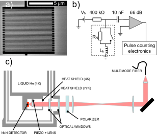
We mounted the SSPD in a 4He-cryostat and cooled it to a temperature of 5 K. The temperature remained constant within 10 mK during each measurement run. Figure 1(b) shows a schematic overview of the electronic circuit used to operate the detector. The detector was biased at 90% of the critical current through a bias-T with a 400 k resistor. The equivalent circuit of the detector (dashed box) contains a switch that is closed in the superconducting state. When a photon is absorbed, the switch opens temporarily Kerman et al. (2006). The resulting voltage pulse across the detector is amplified (66 dB) and detected by pulse counting electronics.
Unpolarized light from an incandescent tungsten lamp was wavelength-filtered and sent through a 50 m core size multimode optical fiber. The output of the fiber was imaged onto the detector using a telescope and a lens mounted on a piezo stage inside the cryostat, as shown in Fig. 1(c). To probe the polarization dependence of the detection efficiency, a linear polarizer with an extinction ratio better than for the wavelength range of interest was placed in the parallel part of the beam. To probe the wavelength dependence, we used different narrow bandpass filters (10 nm FWHM) in combination with several edge filters to ensure that the light on the detector was monochromatic.
III Polarization dependence
Figure 2 shows the count rate of the detector as a function of linear polarization for a wavelength of 1550 nm (black squares) and 532 nm (red triangles). Note that the absolute count rates at different wavelengths cannot be compared directly, due to a difference in incident power. The insets show the orientation of the -field relative to the detector. The measured count rates follow a sinusoidal dependence as a function of polarization and are minimal when the -field is perpendicular to the lines of the detector.
We define the polarization contrast as
| (2) |
where and are the count rates of the detector when the light is polarized parallel and perpendicular to the wires, respectively. This definition of the contrast is a direct measure for the polarization effects, independent of the electronic quantum efficiency (), and the incident power. We extract the contrast from the sinusoidal fits to the data (solid curves in Fig. 2). It varies with the wavelength of the incident light and is independent of the bias current and temperature of the detector in our experiment.
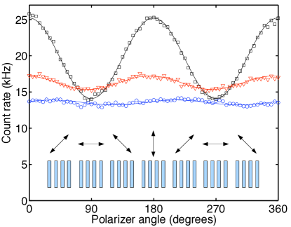
The blue circles in Fig. 2 show the count rate as a function of polarizer angle, at a wavelength of 1550 nm, when two wedge depolarizers under a relative angle of 45∘ were placed after the polarizer. These wedge depolarizers effectively depolarize the incident light by imposing a position-dependent rotation of the polarization. Indeed, the polarization contrast in this case is reduced to below . The lower average count rate can be attributed to the extra four air-glass interfaces in the optical setup, leading to an increased reflection of the incident light.
The polarization effect can be understood by comparing the periodic structure of the detector to that of a wire grid polarizer Bird and Parrish (1960) that consists of a grid of parallel, highly conductive metal wires with a subwavelength spacing. For a perfect conductor the -field should be perpendicular to the metal surface. As a consequence, only light with a polarization perpendicular to the wires is efficiently transmitted. A similar argument holds for lossy metals, albeit that in this case the field penetrates into the metal, leading to absorption. This absorption is largest when the -field is parallel to the wires, since in this case the field penetrates more into the metal.
For the typical dimensions and spacing of the NbN wires, an effective medium approach that is accurate for both polarizations is difficult Aspnes (1982); Pitarke and Garcia-Vidal (1998). Instead, we calculated the absorption at normal incidence for an infinitely-sized detector, using the rigorous coupled-wave analysis (RCWA) developed in Ref. 14. This method finds an exact solution of Maxwell’s equations by expressing the electromagnetic fields in the different materials as a summation over all diffraction orders. The Fourier components of the periodic dielectric constant couple the diffraction orders in the patterned region. The continuity of the parallel component of the wavevector, together with the boundary conditions for the and fields fully determine the field in all regions. From this the intensity in all reflected and transmitted diffraction orders can be calculated. The absorption in the grating is then simply given by , where and are the reflected and transmitted intensity.
The effects of focusing of the incident beam can be taken into account by decomposing the beam into plane waves with wave vector . Each of these plane waves will experience a different absorption . The effect of finite detector size can be incorporated in a similar way, by multiplying the beam profile in the near field by an aperture function which is 1 at the location of the detector, and 0 elsewhere. Taking both into account, the total absorption is given by the convolution integral
| (3) |
where is the Fourier transform of the beam profile, and is the Fourier transform of the aperture function .
The -spread of the incident waves is determined by the detector size [determining the spread in ] and the numerical aperture of the last lens in the illuminating system, determining the spread in . The latter is the most important factor in our experiment, since we used a large-NA lens to focus the incoming light onto the detector. Calculations of the absorption of the grating as a function of angle of incidence (i.e., as a function of ) show however, that the absorption only varies appreciably from the absorption at normal incidence for angles of incidence corresponding to . Therefore, the total absorption given by Eq. (3) can be approximated by a product of the absorption coefficient at normal incidence and the total intensity impinging on the (finite-sized) detector. This justifies the use of a plane wave calculation in the rest of this Paper.
To calculate the absorption efficiency, we used the nominal structure parameters of the detector, and tabulated values of the dielectric constant of the sapphire substrate ( at 1550 nm) Palik (1998). For the wavelength-dependent dielectric constant of NbN, a Drude model Tanabe et al. (1988) was used, giving a refractive index at a wavelength of 1550 nm. This value is close to the value reported in Ref. 7, for a thicker NbN film.
Figure 3(a) shows the calculated absorption for polarization parallel (blue line) and perpendicular (red line) to the wires, as a function of wavelength. The absorption for parallel-polarized light monotonously increases with wavelength, whereas the absorption for perpendicular polarization goes through a maximum and decreases for wavelengths above nm. This leads to a higher polarization contrast for longer wavelengths.
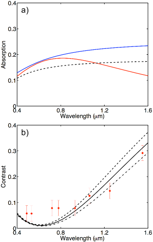
For comparison, the dashed line in Fig. 3(a) shows the absorption of an unpatterned film, multiplied by the filling factor of NbN, as was suggested in Ref. 1. This estimate deviates over the entire wavelength range from the polarization-averaged result obtained by RCWA, which shows that for structures with features smaller than the wavelength of light, a more refined model is needed. We will discuss this refined model in Sec. IV. The fact that the absorption decreases for both the parallel polarization and for the closed film is mostly due to dispersion of the dielectric constant of the NbN material, .
In Fig. 3(b) we compare the measured polarization contrast (red dots) to the results of the calculations (black solid curve), as a function of wavelength. For comparison, the calculated contrast is shown for filling factors of 52% (dashed curve) and 58% (dash-dotted curve) as well. The experimentally observed contrast varies between 5% and 30% and increases with wavelength. The error bars on the experimental points represent slight variations in the measured polarization contrast during different measurement runs, as well as a slight polarization in the illuminating light source, of . We attribute the fact that the calculation and the measurements differ for lower wavelengths to the fact that we used literature values for the dielectric constant of NbN. It is known that the dielectric constant of NbN varies as a function of the deposition parameters Tanabe et al. (1988) and may depend on the film thickness as well Lee et al. (2008). Additional calculations (not shown) reveal, that for lower wavelengths, the polarization contrast is increasingly sensitive to small variations in the dielectric constant of NbN.
It has been shown that the linear-polarization dependence can be removed by changing the design of the detector Dorenbos et al. (2008). A spiraling detector breaks the translational symmetry that causes the strong polarization contrast. The optical absorption in such a detector, however, will be lower than the maximum obtainable for parallel-polarized light, due to the fact that in these detectors, partial screening of the electric field is always possible.
IV Discussion
IV.1 An optical impedance model for the absorption of a metal film
In order to gain some physical insight into the absorption in the detector, we start out by describing the absorption of a film of thickness with a complex dielectric constant , embedded between two dielectrics with refractive index and , respectively. The film is illuminated from the medium with index .
We can define the optical impedance of a medium with refractive index as
| (4) |
where is the impedance of the vacuum. The reflection and transmission of the layered system are given by Ramo and Whinnery (1953)
| (5) | |||||
| (6) |
where is the combined load impedance of the film and the backing substrate. The absorption of the film is again given by .
If we assume that the film is thin enough to neglect interference effects (), the load impedance is given by Kornelsen et al. (1991)
| (7) |
where is the square resistance for a highly absorbing () film, and is the wave vector of the light in vacuo. With these assumptions, we can write the absorption in the film as
| (8) |
The absorption of the film reaches a maximum value for a square resistance given by
| (9) |
Note that the maximum possible absorption is a function of the refractive indices of the surrounding media only. The optimal value of to reach this maximum can be obtained by tuning the film thickness .
IV.2 The effect of film thickness
Figure 4 shows the absorption and the polarization contrast of a film of NbN, embedded between air () and sapphire (), as a function of the film thickness. The solid curves show the calculated absorption using the rigorous coupled-wave analysis described before, while the dotted curves are obtained from the impedance model.
For a closed film (black curves), there is a distinct maximum of absorption, that occurs at a thickness
| (10) |
For thinner films, the transmission through the film is too high to get maximal absorption, whereas for thicker films, reflection dominates.
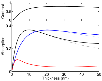
The blue and red curves in Fig. 4 show the absorption for a detector with filling factor 0.5 and lattice period 200 nm, for polarization parallel and perpendicular to the wires, respectively. The thickness for which the absorption in the patterned film is maximum, is higher than the optimal thickness for the closed film. The dotted line is calculated using the impedance model of section IV.1, taking an effective dielectric constant for the absorbing film, given by Aspnes (1982)
| (11) |
where is the filling factor of the metal, and is the dielectric constant of the material in the slits, typically air. Since only the imaginary part of determines the absorption in the film, the absorption of the detector can simply be calculated by multiplying the thickness of the film by the filling factor. For the polarization perpendicular to the wires of the detector, it is not so straightforward to define an effective dielectric constant for the patterned film Aspnes (1982); Pitarke and Garcia-Vidal (1998). For this polarization the light is concentrated in the air slits and the effective dielectric constant is closer to that of air. Therefore the condition used to define the impedance model, breaks down for this polarization.
Surprisingly, the calculation also shows that it is easily possible to construct a detector where the absorption for parallel polarization is larger than the absorption of an unpatterned film of the same thickness. Since the electronic efficiency of the detector, , strongly depends on the thickness of the metal Verevkin et al. (2004); Jukna et al. (2008), it is important to realize that the absorption for parallel-polarized light is a function of . A reduction in thickness of the detector, to increase the electronic efficiency, can thus be countered by increasing the filling factor accordingly.
IV.3 Illuminating through sub- or superstrate
Commonly, NbN SSPDs are deposited on a substrate of sapphire and illuminated from air. An inspection of Eq. (8) shows that for a certain choice of sub- and superstrate, a factor of in absorption can be gained by illuminating the detector from the medium with the higher refractive index. Figure 5 shows the calculated absorption for a detector, with a superstrate of air , as a function of the refractive index of the substrate. The thickness of the detector is set such that maximal absorption in the detector is achieved. This thickness is indicated with the black line. The solid curves give the absorption for illumination from the air, whereas the dash-dotted curves give the absorption for illumination from the substrate. The blue and red curves are for polarization parallel and perpendicular to the wires, respectively. We stress that this effect is caused by a lower impedance mismatch and should be separated from the cavity enhancement of the absorption, previously reported in Refs. Rosfjord et al. (2006); Anant et al. (2008).
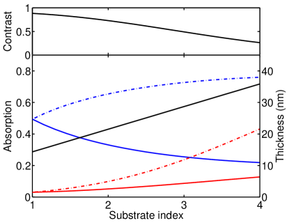
When the substrate index is increased, the absorption rises for illumination from the substrate side. For illumination from the air side, the absorption for parallel polarization decreases. Note however that in both cases, the polarization contrast decreases, from at to at , and is independent on the direction of illumination, as shown in the top graph of Fig. 5. The absorption is a factor of higher, when the detector is illuminated from the substrate, as expected from the impedance model. It is interesting to note that, for parallel-polarized light, the absorptions from super- and substrate add up to give . It is therefore possible to construct a detector with higher absorption, up to 70%, and lower polarization contrast, by using a high refractive index substrate (e.g. Si or GaAs) and illuminating the detector from the substrate. Unfortunately, increasing the refractive index of the substrate also increases the wavelength for which diffraction orders in the substrate appear. The first diffraction order at normal incidence appears at , with the periodicity of the structure, and the wavelength of the light. In general, these diffraction orders lower the absorption efficiency. For a typical lattice period of 200 nm, and a substrate index of , the first diffraction order appears at a wavelength of 700 nm, making detectors on a high-refractive-index substrate less effective for detecting visible light. The problem of diffraction could also be circumvented by designing a detector that has a variable line spacing.
V Conclusion
In conclusion, we have measured a polarization dependence in the detection efficiency of NbN superconducting single photon detectors and find a wavelength dependent polarization contrast between 5% and 30%. This effect can be explained by the geometry of the detector. Calculations of the optical absorption efficiency give good agreement with the measured data. We have demonstrated that the polarization dependence can be removed by the use of wedge depolarizers.
Furthermore, we have shown that the parameters of the detector can be tuned to achieve an absorption for a polarization parallel to the detector wires, that exceeds the absorption of an unpatterned film of the same thickness. We have given a simple optical impedance model, that allows for a quick estimate of the parameters needed to optimize the detector. For parallel-polarized light, the maximum absorption achievable is not determined by the thickness or the dielectric constant of the metal film, nor by the filling factor, but only by the refractive indices of the surrounding media. We have shown that by illuminating the detector from the substrate it is possible to increase the detection efficiency of the detector even further, by a factor equal to the refractive index of the substrate. Such highly absorbing, highly polarization-dependent detectors can be employed to efficiently detect photons with a well-defined polarization.
Acknowledgments
We thank Jos Disselhorst, Jennifer Kitaygorsky, Teun Klapwijk, Hans Mooij, and Raymond Schouten for technical assistance and discussions. This research was financed by the Dutch Foundation for Scientific Research (NWO) and the Foundation for Fundamental Research of Matter (FOM).
References
- Gol’tsman et al. (2001) G. N. Gol’tsman, O. Okunev, G. Chulkova, A. Lipatov, A. Semenov, K. Smirnov, B. M. Voronov, A. Dzardanov, C. Williams, and R. R. Sobolewski, Appl. Phys. Lett. 79, 705 (2001).
- Gol’tsman et al. (2007) G. N. Gol’tsman, O. Minaeva, A. Korneev, M. Tarkhov, I. Rubtsova, A. Divochiy, I. Milostnaya, G. Chulkova, N. Kaurova, B. M. Voronov, et al., IEEE Trans. Appl. Supercond. 17, 246 (2007).
- Takesue et al. (2007) H. Takesue, S. W. Nam, Q. Zhang, R. H. Hadfield, T. Honjo, K. Tamaki, and Y. Yamamoto, Nat. Photon. 1, 343 (2007).
- Semenov et al. (2003) A. Semenov, A. Engel, K. Il’in, G. N. Gol’tsman, M. Siegel, and H.-W. Hübers, Eur. Phys. J.-Appl. Phys. 21, 171 (2003).
- Kerman et al. (2006) A. J. Kerman, E. A. Dauler, W. E. Keicher, J. K. W. Yang, K. K. Berggren, G. N. Gol’tsman, and B. M. Voronov, Appl. Phys. Lett. 88, 111116 (2006).
- Ejrnaes et al. (2007) M. Ejrnaes, R. Cristiano, O. Quaranta, S. Pagano, A. Gaggero, F. Mattioli, R. Leoni, B. Voronov, and G. N. Gol’tsman, Appl. Phys. Lett. 91, 262509 (2007).
- Anant et al. (2008) V. Anant, A. J. Kerman, E. A. Dauler, J. K. W. Yang, K. M. Rosfjord, and K. K. Berggren, Opt. Express 16, 10750 (2008).
- Bouwmeester et al. (2000) D. Bouwmeester, A. K. Ekert, and A. Zeilinger, The Physics of Quantum Information (Springer, 2000).
- Engel et al. (2006) A. Engel, A. Semenov, H.-W. Hübers, K. Il’in, and M. Siegel, Physica C 444, 12 (2006).
- Bell et al. (2007) M. Bell, N. Kaurova, A. Divochiy, G. N. Gol’tsman, J. Bird, A. Sergeev, and A. A. Verevkin, IEEE Trans. Appl. Supercond. 17, 267 (2007).
- Rosfjord et al. (2006) K. M. Rosfjord, J. K. W. Yang, E. A. Dauler, A. J. Kerman, V. Anant, B. M. Voronov, G. N. Gol’tsman, and K. K. Berggren, Opt. Express 14, 527 (2006).
- Bird and Parrish (1960) G. R. Bird and M. Parrish, J. Opt. Soc. Am. 50, 886 (1960).
- Aspnes (1982) D. E. Aspnes, Am. J. Phys. 50, 704 (1982).
- Pitarke and Garcia-Vidal (1998) J. M. Pitarke and F. J. Garcia-Vidal, Phys. Rev. B 57, 15261 (1998).
- Moharam et al. (1995) M. G. Moharam, E. B. Grann, D. A. Pommet, and T. K. Gaylord, J. Opt. Soc. Am. A 12, 1068 (1995).
- Palik (1998) E. D. Palik, Handbook of Optical Constants of Solids, vol. III (Academic Press, 1998).
- Tanabe et al. (1988) K. Tanabe, H. Asano, Y. Katoh, and O. Michikami, J. Appl. Phys. 63, 1733 (1988).
- Lee et al. (2008) W.-J. Lee, J.-E. Kim, H. Y. Park, S. Park, M.-S. Kim, J. T. Kim, and J. J. Ju, J. Appl. Phys. 103, 073713 (2008).
- Dorenbos et al. (2008) S. N. Dorenbos, E. Reiger, N. Akopian, U. Perinetti, V. Zwiller, T. Zijlstra, and T. M. Klapwijk, Appl. Phys. Lett. 93, 161102 (2008).
- Ramo and Whinnery (1953) S. Ramo and J. R. Whinnery, Fields and Waves in Modern Radio (John Wiley & Sons, 1953), 2nd ed.
- Kornelsen et al. (1991) K. E. Kornelsen, M. Dressel, J. E. Eldridge, M. J. Brett, and K. L. Westra, Phys. Rev. B 44, 11882 (1991).
- Verevkin et al. (2004) A. Verevkin, A. Pearlman, W. Slysz, J. Zhang, M. Currie, A. Korneev, G. Chulkova, O. Okunev, P. Kouminov, K. Smirnov, et al., J. Mod. Optics 51, 1447 (2004).
- Jukna et al. (2008) A. Jukna, J. Kitaygorsky, D. Pan, A. S. Cross, A. J. Pearlman, I. Komissarov, O. Okunev, K. Smirnov, A. Korneev, G. Chulkova, et al., Acta Phys. Pol. A 113, 955 (2008).