Tunable Band Gap in Graphene with a Non-Centrosymmetric Superlattice Potential.
Abstract
We show that, if graphene is subjected to the potential from an external superlattice, a band gap develops at the Dirac point provided the superlattice potential has broken inversion symmetry. As numerical example, we calculate the band structure of graphene in the presence of an external potential due to periodically patterned gates arranged in a triangular or a square graphene superlattice (TGS or SGS) with broken inversion symmetry, and find that a band gap is created at the original and, in the case of a TGS, the “second generation” Dirac point. This gap, which extends throughout the superlattice Brillouin zone, can be controlled, in principle, by changing the external potential and the lattice constant of the superlattice. For a square superlattice of lattice constant 10 nm, we have obtained a gap as large as 65 meV, for gate voltages no larger than 1.5 V.
I Introduction
Ever since the synthesis of high-quality graphenenovoselov , there has been tremendous interest in the properties of this single-layer form of carbon. Graphene has a honeycomb lattice structure, with two atoms per primitive cell and a hexagonal Brillouin zone (BZ). The Fermi energy of homogeneous, neutral graphene lies at the so-called Dirac point, which occurs at high symmetry points in the BZ. In fact, there are two inequivalent Dirac points and with two distinct valleys of excitations. Near the Dirac point, the density of states is linear in and the spectrum of quasiparticle states is well described by the Dirac equation for massless fermions. Partly as a result of this electronic structurenovoselov ; zhang ; berger ; geim , graphene has many unusual electronic properties, such as a unique type of quantum Hall effectnovoselev1 ; purewal , ballistic conduction by massless Dirac fermionsnovoselev1 ; purewal , size-dependent band gaphan , large magnetoresistancehill ; geim ; cho , and gate-tuneable optical transitionswang .
A number of workers have investigated the possibility of building graphene electronic circuits without physically cutting or etching the graphene monolayer. A natural way to accomplish this is by subjecting graphene to an external potential with a suitable superlattice periodicity, e. g., by applying appropriate gate voltages. Such superlattices have proven to be extremely successful in controlling the electronic structure of more conventional semiconducting materials (see, e. g., Ref. tsu ). In these materials, the presence of the additional periodic potential gives rise to superlattice electronic band structure, which has extra band gaps at high symmetry points in the superlattice Brillouin zone (SBZ).
There have been several predictions of electronic effects in graphene due to an external superlattice potential. For example, with one-dimensional (1D) and two-dimensional (2D) superlattices, the group velocity of the low-energy charge carriers is anisotropically renormalized ar , while a corrugated graphene sheet is expected to show charge inhomogeneity and localized states guinea . Superlattices in graphene can be realized experimentally by using periodically patterned gates. Using an electron-beam, adatoms with a superlattice patterns of periodicity as small as 5 nm have been achieved on freestanding graphene membranes meyer . Superlattice patterns have also been observed for graphene on metal surfaces marchini ; vazquez ; pan . In a recent theoretical study, a triangular graphene superlattice (TGS) was considered, and a new class of massless Dirac fermions was predicted to occur at the M point in the SBZpark .
In the studies so far, the external periodic potential giving rise to the superlattice has had spatial inversion symmetry. As a result of this symmetry, the degeneracy of the conduction and valence band at the original Dirac point (ODP) is preserved. In the present work, by contrast, we consider the potentials of an external TGS and a square graphene superlattice (SGS) without inversion symmetry. We show that, because of the absence of inversion symmetry, an energy gap opens up at both the original and the new Dirac points in the TGS and at the Dirac point in the SGS. The magnitude of these gaps can, in principle, be controlled by modifying the externally applied voltages. Thus far, we have been able to achieve a band gap as large as 65 meV extending throughout the SBZ. Because of the controllability of the band gap, this type of graphene superlattice represents a system in which the band gap can be chosen with considerable freedom by modifying the applied external potential. Such a system, and particularly the control at the ODP, might be quite useful in realizing future graphene electronic circuits.
II Formalism
We first describe the formalism we use to calculate the superlattice band structure for a non-centrosymmetric superlattice potential, mostly following the approach of Ref. park . If the periodicity of the superlattice is much larger than the intercarbon distance 1.42 , which is the case considered here, the intervalley scattering (between K0 and K) can be neglected ando . We limit our discussion to the spectrum near one of the two inequivalent Dirac points, which we denote , in the presence of a periodic external potential . In pure graphene, we use a pseudospin basis and , where and are Bloch sums of orbitals with wave vector on the sublattices A and B, respectively, and is the wave vector relative to the point. The single valley Hamiltonian for the quasiparticles of pure graphene iswallace
| (1) |
where is the (isotropic) group velocity at the Dirac point and the ’s are Pauli matrices. The eigenstates and energy eigenvalues are
| (2) |
and
| (3) |
where is the band index and is the polar angle of the wavevector . Eq. (2) indicates that the pseudospin vector is parallel and antiparallel to in the upper () and lower () bands, respectively.
We wish to consider the spectrum of elementary excitations near one of the Dirac points in the presence of . The total Hamiltonian then takes the form , where
| (4) |
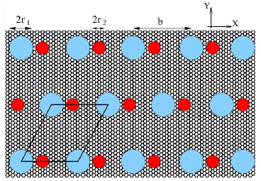
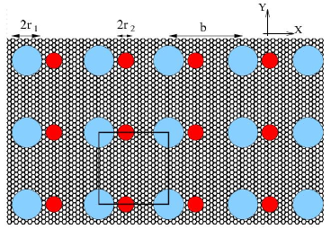
being the identity matrix. We consider a periodic external potential having either a triangular Bravais lattice with basis vectors , , or a square Bravais lattice with , . We also assume that varies slowly on the scale of a lattice constant (). Then the band structure of the elementary excitations near the K0 point can readily be obtained by diagonalizing in a plane wave spinor basispark . The basis states are of the form , where or and is a reciprocal lattice vector corresponding to the periodic external potential . If we include plane waves, we must thus diagonalize a matrix to obtain the band structure of elementary excitations non-perturbatively near the point in the presence of the external periodic potential. We use for both the triangular and the square graphene superlattice. In our actual calculations, we have considered an external potential produced by a periodic array of circular regions, within each of which the potential is a constant. These are easy to treat by the above approach, because the Fourier transform of the constant potential is available analytically. To break the inversion symmetry, we have added a second, smaller circular region within each primitive cell, as illustrated in Figs. 1 and 2. If the second region is not equidistant from the two adjacent larger circular regions, inversion symmetry is broken.
III Results
We first review the case of a triangular array of large circles, with a constant external potential within each circle. Elsewhere in the superlattice, the external potential is zero. The resulting band structure has been computed in Ref. park . In the presence of the superlattice, there are several Dirac points: the ODP, which is at of the SBZ, and “next generation” Dirac points, at and of the SBZ. Of these new Dirac points, only the ODP (with energy set to 0 eV) and the new Dirac point (NDP) at M with energy 0.196 eV) have vanishing density of statespark . Near both of these points, the density of states goes linearly to zero with energy. However, the group velocity near the NDP is highly anisotropic.
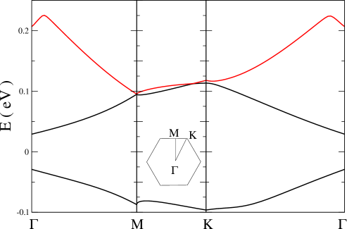
We now consider the superlattice band structure (SBS) for graphene subject to the non-centrosymmetric potential shown in Fig. 1. We choose the lattice constant of the external potential to be nm, and the radius of the large circles to be nm, so that the filling fraction of large circles is 0.226725. We take the smaller circular gates to have radius nm, and to be centered at , where is a Bravais vector of the superlattice. The resulting band structure is shown in Fig. 3 for the case V, V, where and are the voltages on the larger and smaller circles. Once again in the rest of the lattice. A substantial direct gap opens up at the ODP of magnitude meV for these parameters (between the bands above and below the ODP). Although not obvious from Fig. 3, there is also a gap which opens up at the NDP, of magnitude meV. For these parameters, we have checked that there is, in fact, a full band gap at ODP extending through the entire SBZ. The small gap also at does not extend throughout the SBZ, as is evident from the Figure (the gap at does extend throughout the SBZ for positive). The inset of Fig. 3 shows the SBZ, with the symmetry points , , and indicated.
In Fig. 4, we show the corresponding SBS for graphene subjected to the periodic potential with square symmetry shown in Fig. 2. Once again, we choose the superlattice constant nm, nm, and nm, so that the filling fraction of circles in this case is 0.227765. We choose V and V, and each small circle is located at relative to the center of each large circle. There is a gap of magnitude meV, at the ODP at which extends throughout the SBZ.
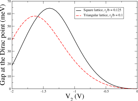
In Fig. 5, we show show how the direct gaps at the Dirac point depend on the voltage on the smaller circles in the triangular and square superlattices. For the square superlattice, we take nm, , at V, and the small circles are located at . For the triangular superlattice, nm, , , V, and the small circles are located at . In both cases, these gaps show clear maxima as functions of . We have carried out similar calculations using positive values of in both cases and also obtain nonzero gaps extending throughout the SBZ. In the case of positive , they are generally smaller than for negative voltages.
In Fig. 6, we show the dependence of the gaps at the Dirac point on the radius in both the triangular and square superlattices. For the square superlattice, we take nm, V, V, and the small circles are located at . For the triangular case, nm, V, V, , and we locate the small circular contacts at . The direct band gaps can reach as large as 65 meV for the square superlattice.
Because of the special form of the Hamiltonian of eqs. (1) and (4), the superlattice band structure, and hence the band gap at the ODP, exhibits a simple scaling relation: under the transformation and , where is a dimensionless scaling factor, the eigenvalues of satisfy . Thus, in particular, is multiplied by . For example, if is halved (and all other lengths are also halved), and the potentials on all the contacts are doubled, then the band gap is also doubled. We have confirmed numerically that this scaling relation is satisfied for our bands.
Besides these calculations, we have tried some other geometries in an effort to obtain the largest possible band gap. For example, we have calculated the SBS for triangular and square superlattices with two off-center circular contacts, one along each edge of the primitive cell. This geometry does not lead to band gaps larger than we have obtained with one off-center circle.
IV Discussion
The present results show that the band gap of graphene at the Dirac point can be manipulated by subjecting it to a superlattice potential which lacks inversion symmetry. The magnitude of the band gap can be controlled by modifying the contact potentials. Thus, if such an arrangement of contacts can be created, the resulting material has a band gap which can be controlled via the applied voltages without modifying the structure.
There are several obvious challenges before this scheme could be used in practice. First, the band gaps are rather small (of order 65 meV). These can be made larger by reducing , while simultaneously increasing and as implied by the above scaling relation, but this could be challenging experimentally. The gaps can also be increased by increasing the voltages at fixed geometry. Perhaps the most promising scheme might be to increase while simultaneously increasing the bias voltages. The larger would be easier to achieve experimentally, while the large voltage offsets would increase the gap. These ideas certainly do not exhaust the possibilities offered by periodic arrangements of contacts. Any 2D superlattice of gates lacking inversion symmetry would lead to a band gap at the ODP, and some which we have not tried may lead to a larger band gap than those we have found to date. A 1D superlattice potential lacking inversion symmetry will not suffice to produce a complete band gap. But such a 1D potential, when combined with a suitable non-time-reversal-invariant perturbation such as a magnetic field, might also lead to a complete band gap.
There are, of course, many other ways to create a band gap in graphene besides the method described here. For example, one could create a non-centrosymmetric lattice of nanoscale holes in graphene. It would be difficult to use this method, however, to create a tunable band gap. In graphene nanoribbons with armchair edges, the band structure becomes insulating if the width of the sample, in units of the lattice constant , is not of the form , with an integerbreyfertig ; son ; ezawa ; barone ; chen . But creating such a ribbon requires cutting graphene samples with very high precision, and again, once the ribbon has been created, the band gap cannot be easily tuned. Other possibilities are to induce a gap by using a substrate which lacks inversion symmetrygiovannetti , or to use graphene antidot latticespedersen Again in this case, the gap cannot easily be controlled because the atomic spacing of the substrate is fixed. Our proposal of a TGS (or other 2D superlattice) with a non-centrosymmetric superlattice potential is more efficient in opening up a gap at the ODP. In principle, moreover, this gap can easily be larger than the thermal energy at room temperature for modest values of potential. Thus, this method may be a viable approach to creating graphene with a readily tunable band gap.
In summary, we have calculated the superlattice band structure for graphene subjected to a non-centrosymmetric superlattice of contacts, on each of which the voltage is held constant. We find that the superlattice band structure exhibits a band gap extending throughout the SBZ, which can thus be tuned by external voltages. For some choices of the voltages and superlattice constant, the band gap can be as large as meV, significantly larger than the room temperature thermal energy. Thus, this arrangement might possibly be of use in future electronic or electromagnetic devices.
V Acknowledgments
This work has been supported in part by NSF DMR-0820414 through the Materials Research Science and Engineering Center at Ohio State University. We acknowledge valuable conversations with J. P. Pelz.
References
- (1) K. S. Novoselov, A. K. Geim, S. V. Morozov, D. Jiang, M. I. Katsnelson, I. V. Grigorieva, S. V. Dubonos and A. A. Firsov, Nature (London) 438, 197 (2005).
- (2) Y. Zhang, J. W. Tan, H. L. Stormer and P. Kim, Nature (London) 438, 201 (2005).
- (3) C. Berger, Z. Song, X. Li, X. Wu, N. Brown, C. Naud, D. Mayou, T. Li, J. Hass, A. N. Marchenkov, E. H. Conrad, P. N. First, W. A. de Heer, Science 312, 1191 (2006).
- (4) A. K. Geim and K. S. Novoselov, Nature Mater. 6, 183 (2007).
- (5) V. S. Novoselev, A. K. Geim, S. V. Morozov, D. Jiang, M. I. Katsnelson, I. V. Grigorieva, S. V. Dubonos and A. A. Firsov, Nature 438, 197 (2005).
- (6) M. S. Purewal, Y. Zhang, and P. Kim, Phys. Stat. Solidi B 243, 4318 (2006).
- (7) M. Y. Han, B. Ozyilmaz, Y. Zhang, and P. Kim, Phys. Rev. Lett. 98, 206805 (2007).
- (8) E. W. Hill, A. K. Geim, K. S. Novoselev, F. Schedin,and P. Blake, IEEE Trans. Magn. 42, 2694 (2008).
- (9) S. Cho and M. S. Fuhrer, Phys. Rev. B 77, 081402(R) (2008).
- (10) F. Wang, Y. Zhang, C. Tian, C. Girit, A. Zettl, M. Crommie, and Y. R. Shen, Science 32], 206 (2008).
- (11) R. Tsu, Superlattice to Nanoelectronics ( Elsevier, Oxford, 2005).
- (12) C.-H. Park et al., Nature Phys. 4, 213 (2008); M. Barbier, F. M. Peeters, P. Vasilopoulos and J. M. Pereira, Jr., Phys. Rev. B 77, 115446 (2008).
- (13) F. Guinea, M. I. Katsnelson and M. A. H. Vozmediano, Phys. Rev. B 77, 075422 (2008).
- (14) J. C. Meyer, C. O. Girit, M. F. Crommie and A. Zettl, Appl. Phys. Lett. 92, 123110 (2008).
- (15) S. Marchini, S. Günther and J. Wintterlin, Phys. Rev. B 76, 075429 (2007).
- (16) A. L. Vazquez de Parga, F. Calleja, B. Borca, M. C. G. Passeggi, Jr., J. J. Hinarejos, F. Guinea and R. Miranda, Phys. Rev. Lett. 100, 056807.
- (17) Y. Pan et al., arXiv:0709.2858v1.
- (18) C.-H. Park, L. Yang, Y.-W. Son, M. L. Cohen, and S. G. Louie, Phys. Rev. Lett. 101, 126804 (2008)
- (19) T. Ando and T. Nakanishi, J. Phys. Soc. Jpn. 67, 1704 (1998).
- (20) P. R. Wallace, Phys. Rev. 71, 622 (1947).
- (21) L. Brey and H. A. Fertig, Phys. Rev. B 73, 235411 (2006).
- (22) Y.-W. Son, M. L. Cohen, and S. G. Louie, Phys. Rev. Lett. 97, 216803 (2006).
- (23) M. Ezawa, Phys. Rev. B 73, 045432 (2006).
- (24) V. Barone, O. Hod, and G. E. Scuseria, Nano Letters 6, 2748 (2006).
- (25) Z. Chen, Y.-M. Lin, M. J. Rooks, and P. Avouris, Physica E 40, 228 (2007).
- (26) G. Giovannetti, P. A. Khomyakov, G. Brocks, P. J. Kelly, and J. van den Brink, Phys. Rev. B 76, 073103 (2007).
- (27) T. G. Pedersen, C. Flindt, J. Pedersen, N. A. Mortensen, A.-P. Jauho, and K. Pedersen, Phys. Rev. Lett. 100, 136804 (2008).