Development of Vertically Integrated Circuits for ILC Vertex Detectors
Abstract
We report on studies of vertically interconnected electronics (3D) performed by the Fermilab pixel group over the past two years. These studies include exploration of interconnect technology, backside thinning and laser annealing, the production of the first 3D chip for particle physics, the VIP, and plans for a commercial two-tier 3D fabrication run. Studies of Direct bond Interconnect (DBI) oxide bonding and Silicon-on-Insulator based technologies are presented in other talks in this conference.
1 3D electronics
3D electronics is generally defined as consisting of multiple layers of electronics, thinned, bonded and interconnected to form a monolithic circuit. This technology has become an area of intense focus in the electronics industry as a way to improve circuit performance without the expense and complexity of smaller feature size [2] [3]. 3D electronics provides the ability to integrate heterogeneous technologies, reduce interconnect lengths, and expand bus width. These technologies are particularly interesting for pixel detectors, where they offer new techniques for integrating sensors and electronics, and provide substantially more processing power per pixel than conventional technologies.
Fabrication of a 3D stack depends on the development of several techniques including:
-
•
Bonding between layers including oxide to oxide fusion, copper/tin bonding, copper/copper bonding, polymer/adhesive bonding
-
•
Wafer thinning using grinding, lapping, etching, and Chemical Mechanical Polishing (CMP)
-
•
Through wafer via formation and metalization either with isolation using Through Silicon Vias (TSVs) or without isolation as in Silicon-on-Insulator (SOI) devices.
-
•
High precision alignment
The technology can also be separated into techniques which form the via before 3D integration is performed (via first) and those which form vias afterwards (via last).
2 VIP Chip
The VIP chip [5] was intended as a demonstration of 3D technology as applied to an ILC vertex detector. It was fabricated in 0.18 micron SOI CMOS technology by MIT-Lincoln Labs as part of a DARPA-sponsored multiproject run. The chip consists of three tiers of electronics interconnected by 3D vias. The MIT-LL technology utilizes oxide bonding to bond tiers together. This wafer bonding technology mates activated, planarized silicon oxide surfaces to form a robust inter-wafer bond [4]. The top ”handle” silicon in the bonded wafer stack is thinned to and the remainder of the silicon is etched away to expose the oxide surface. Vias are then formed by etching thorough the insulating oxide to contact internal metalization layers. The process is repeated to form the required number of tiers.
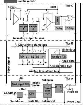
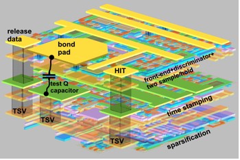
The VIP incorporates an amplifier/disriminator with double correlated sample and hold in tier three, both a 5-bit digital and an analog time stamp in tier 2, and sparsification and digital logic in tier one, all within a square pixel. In ILC operation time stamped hits are stored within the pixel during the bunch train. The chip utilizes part of the 199 ms period between trains for readout, while the front end current is reduced to save power. The front end is designed to consume less than 4 mW/mm where is the front end duty factor. A token passing readout scheme stores addresses on the periphery, minimizing the logic on the pixel. Figure 1 shows a schematic of the chip as well as a visualization of the metal layers.
The chip was submitted in October 2006 and received in October 2007. Initial tests showed that the overall yield was low, with only a few chips showing the ability to propagate the readout token through the full 64 x 64 matrix. The single best-performing chip was selected for full testing. Figure 2 shows the results of the most complete system test, where a pattern of test pulses are injected into the front-end amplifiers, and a sparse scan is performed, reading out those channels where the discriminator fired and latched the readout flag.

Our testing has demonstrated the basic functionality of the chip including propagation of the readout token, threshold scans, input test charge scans, verification of digital and analog time stamping, full sparsified data readout, and fixed pattern and temporal noise measurements. No problems could be found associated with the 3D vias between tiers. Although the chip was fully functional, we were not fully satisfied with yield and performance. Performance problems stemmed from large leakage currents in the protection diodes and transistors, and poor matching of current mirrors. Many of these issues can be traced to the sensitivity of mixed mode designs in fully depleted SOI to the transistor environment and process variations [6] [7]. Intrinsic SOI process problems were exacerbated by our aggressive design, which made extensive use of minimum feature size transistors and dynamic logic, which is sensitive to transistor leakage current.
An new version of the chip, the VIP2, was submitted to the third DARPA sponsored 3D multiproject run in October 2008. As a result of useful interaction with MIT-LL on SOI analog design the overall quality should be considerably improved. Changes to the chip include:
-
•
Different power and grounding layout
-
•
Larger transistor sizes () equivalent feature size
-
•
Larger pixels (30 x 30 microns)
-
•
Redundant vias and larger traces in critical paths
-
•
Redesign of current mirrors to reduce thermal effects
-
•
Removal of dynamic logic due to leakage current problems
Changes were also made to improve the overall functionality including increasing the digital time stamp from 5 to 7 bits. We expect that the changes will lead to a much more reliable chip which can be bonded to sensors for test beam studies.
3 Commercial 3D Technologies
An R&D process, such as the one provided by MIT-LL has disadvantages of long turn-around time and process uncertainties. We are now exploring alternative 3D processes implemented as part of a high volume commercial process. Tezzaron (Naperville Ill) has developed a 3D technology implemented in the high volume 0.13 micron Chartered (Singapore) process [3]. This is a ”via first” process where through-silicon ”supercontacts” are formed after transistor fabrication but before any metalization processing. The 6 micron deep by 1 micron diameter supercontacts are filled with tungsten at the same time as the transistor contacts are formed. Wafers are finished normally, however there is a top layer of thin patterned copper which forms both the bond between wafers and the wafer-to-wafer electrical interconnection. Wafers are then bonded face-to-face with moderate pressure and temperature. Silicon on the top wafer is ground down to the supercontacts and the contacts are metalized to form either external bond pads or to provide connections to the next tier.
Fermilab is organizing a multiproject run in the Tezzaron/Chartered process with submission expected in Spring of 2009. The run includes designs from 13 institutes. The Fermilab designs will include a two tier version of the VIP chip, the VIP2b, as well as test devices for the CMS upgrade and X-ray imaging. Standard commercial CMOS should provide a reliable process with low noise, multiple transistor options, better rad hardness, less wasted via area, faster turn-around, as well as the availability of full wafers for sensor integration.
4 Sensor Integration
The bonding, thinning and lithography process used to build 3D tiers can also be used for sensor integration with readout. Both Tezzaron and Ziptronix provide 3D processes, based on copper-copper and oxide bonding respectively, which can be used to include sensors as a base tier in a 3D stack. 3D processes offer finer pitch and more robust mechanical interconnection than is available in solder-based bump bonding. The high planarity and strong interlayer bonds allow bonded readout ICs to be thinned to 25 or less, which can provide access to integrated through-silicon vias.
We have explored two sensor bonding techniques: Cu-Sn and DBI oxide bonding. The DBI technique is described in another contribution to this conference [8]. We have contracted with RTI to explore Cu-Sn bonding with sparse contacts to minimize contact mass. These technologies do not have the contact bridging problems that limit pitch for solder bumps. However they are not self-aligning which requires special care in aligning the bonded surfaces. In that study successful Cu and Cu-Sn bump structures were fabricated that were compatible with I/O pitch. Electrical tests indicated that the bonding yield was % for both metallurgies. Samples were also destructively tested to evaluate bond strength. In both cases the bond strength is considerably higher than comparable solder bump arrays [9].
5 Thinning and Laser Annealing
Wafer thinning is an important part of 3D technology, and the ability to process and handle thinned silicon is crucial to the goal of constructing a very low mass vertex detector. In some 3D and SOI technologies it will be important to thin the devices after topside processing. After thinning a backside contact ohmic contact must also be formed. The contact is usually fabricated by a high temperature anneal of an ion implantation. This high temperature step is unacceptable for fully processed electronics, where the temperature must be kept below 450 degrees C. to protect the topside metalization.
We have developed a thinning/implantation/annealing process which limits the maximum temperature of the topside to below 100 deg C. The wafer is first bonded to a pyrex carrier using a 3M UV release adhesive designed for wafer thinning applications. The wafer is then thinned and polished using standard techniques. The bonded wafer is ion implanted, taking care to ground the silicon edges and controlling the implantation rate to limit the temperature. The implantation is then annealed using a eximer laser system which melts the silicon locally on the backside to a depth of nm, keeping the topside close to room temperature.
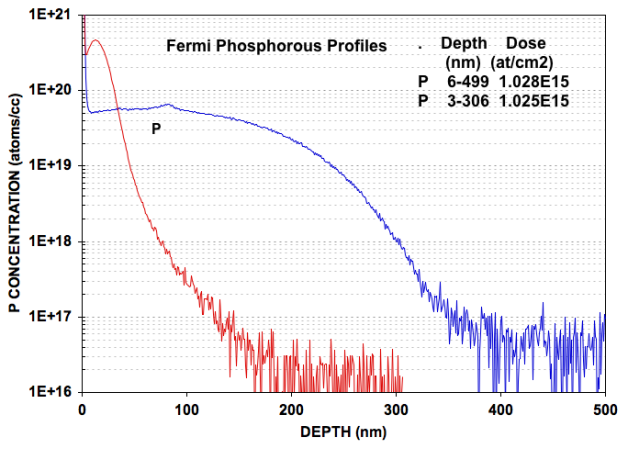
Initial studies were performed using individual strip sensors, which were thinned to remove the backside ohmic implant, re-implanted and laser annealed. All of these devices showed acceptable performance at depletion, with some variation of leakage current depending on laser dose and annealing environment. A scan of the dopant concentration before and after the annealing process is shown in Figure 3. This work was followed by studies using 6” test wafers donated by Micron Semiconductor. These wafers were thinned to 50 microns on the pyrex handle, implanted and laser annealed at MIT-Lincoln Labs. Depletion voltage was reduced from 80 to 2.5 volts with acceptable leakage current. Work is ongoing at Cornell to determine the optimal implantation and annealing parameters.
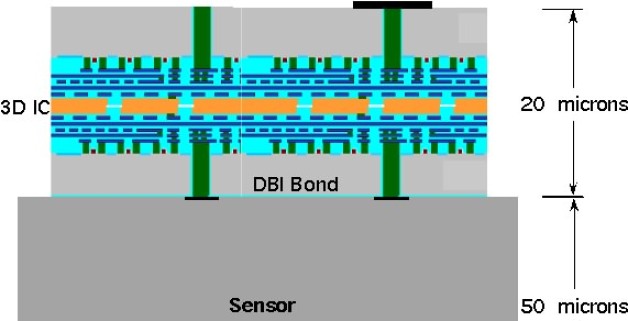
6 Ladder design
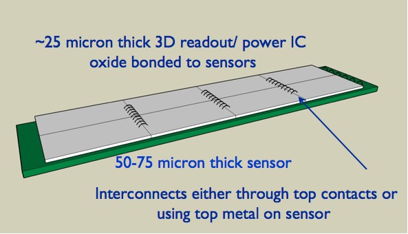
3D technologies provide the ability to construct a low mass, dense, tiled array of chips, which can be used to fabricate ladder and disk planes for the ILC. Figure 4 shows an example of such a structure. Multi-tier readout ICs are fabricated utilizing through-silicon vias. These ICs are bonded to an independently fabricated sensor wafer with a fine pitch technology such as DBI or cu-cu. Once bonded, the Readout ICs are thinned to reveal the topside TSVs. Topside interconnections are patterned using standard lithography and wirebond or other contacts are made. Connections to external power and signal cables could be made at the ends of the sensor, which could have the appropriate interconnection patterns. This technique has a number of advantages:
-
•
The sensor can be a fully depleted detector with charge collection by drift rather than diffusion.
-
•
The sensor wafer serves as a base for the ROICs, obviating the need for reticle stitching.
-
•
The 3D ROICs can include power control tiers.
-
•
Known good ROIC die can be used.
Final sensor thinning would have to occur after the topside processing. This could be done by backgrinding a sensor with an imbedded ohmic contact, either as part of an epitaxial stack or using the SOI technique demonstrated by the Max Plank Institute [10]. This would avoid the additional implant and laser annealing steps needed if the backside were not pre-processed.
7 Conclusions
Fermilab has produced and tested the VIP, the first 3D chip designed for particle physics applications. The chip demonstrated the required functionality but suffered from low yield and compromised performance. An improved version of the chip has been submitted to MIT-LL. The VIP2b, a two-tier 0.13 micron CMOS chip implemented in the Tezzaron 3D process, will be submitted this spring. This submission will extend the development of this technology to applications at super-LHC and in x-ray imaging. We are continuing to develop wafer thinning, interconnection, and post-processing technologies aimed at demonstrating the ability to build precise, low mass, low power vertex detector systems.
References
-
[1]
Presentation:
http://ilcagenda.linearcollider.org/contributionDisplay.py?contribId=42&sessionId=8&confId=2628 - [2] IBM Journal of Research and Development, Volume 52, No. 6, 2008. Issue devoted to 3D technology.
- [3] Philip Garrou, Christopher Bower, Peter Ramm, Handbook of 3D Integration Technology and Applications of 3D Integrated Circuits, Wiley-VCH, 2008.
- [4] IEEE Transactions on Electron Devices, Vol. 53, No. 10, October 2006.
- [5] A Vertically Integrated Pixel Readout Device for the Vertex Detector at the International Linear Collider, FERMILAB-PUB-08-564
- [6] M. Connell et al., 2007 IEEE/SEMI Advanced Semiconductor Manufacturing Conference.
- [7] Tenbroek et al., Solid-State Circuits Conference, 1997, pp. 276-279, 16-18 Sept. 1997.
-
[8]
http://ilcagenda.linearcollider.org/contributionDisplay.py?contribId=207&sessionId=21&confId=2628 - [9] Allan Huffman, Fabrication, Assembly, and Evaluation of Cu-Cu Bump bonding Arrays for Ultra-fine Pitch Hybridization and 3D Integration, Pixel 2008, Fermilab, Batavia, Illinois, September 22-26, 2008.
- [10] P. Fischer et al., Nucl. Instrum. Meth. A 582, 843 (2007).