Graphene Bilayer Field-Effect Phototransistor for Terahertz and Infrared Detection
Abstract
A graphene bilayer phototransistor (GBL-PT) is proposed and analyzed. The GBL-PT under consideration has the structure of a field-effect transistor with a GBL as the channel and the back and top gates. The positive bias of the back gate results in the formation of conducting source and drain sections in the channel, while the negatively biased top gate provides the potential barrier which is controlled by the charge of the photogenerated holes. The features of the GBL-PT operation are associated with the variations of both the potential distribution and the energy gap in different sections of the channel when the gate voltages and the charge in the barrier section change. Using the developed GBL-PT device model, the spectral characteristics, dark current, responsivity and detectivity are calculated as functions of the applied voltages, energy of incident photons, intensity of electron and hole scattering, and geometrical parameters. It is shown that the GBL-PT spectral characteristics are voltage tuned. The GBL-PT performance as photodetector in the terahertz and infrared photodetectors can markedly exceed the performance of other photodetectors.
pacs:
73.50.Pz, 73.63.-b, 81.05.UwI Introduction
At present, infrared detectors are mostly based on narrow-gap semiconductors utilizing the interband transitions. Technologies utilizing HgCdTe and InSb are well developed for infrared detection and imaging 1 ; 2 . The necessity of further extension of the wavelength range covered by photodetectors and imaging devices on their base, widening of their functionality, as well as cost reduction of the production by using a mature processing technology has stimulated the development of quantum-well infrared photodetectors (QWIPs) based on A3B5 compound systems and SiGe alloys and utilizing intersubband (intraband) transitions (see, for instance, 2 ; 3 ). Quantum-dot and quantum-wire infrared photodetectors (QDIPs and QRIPs) were also proposed 4 ; 5 and realized by many groups. The utilization of graphene layers and graphene bilayers 6 ; 7 opens up real prospects in the creation of novel photodetectors. The most important advantage of graphene relates to the possibility to control in a wide range the energy gap by patterning of the graphene layer into an array of narrow strips (nanoribbons) 8 ; 9 . The energy gap in graphene bilayers can be varied by the transverse electric field 10 ; 11 ; 12 ; 13 in different gated heterostructures. The graphene-based photodetectors can exhibit relatively high quantum efficiency (due to the use of interband transitions) and be easily integrated with silicon readout circuits. A photodetector for terahertz (THz) and infrared (IR) radiation based on a field-effect transistor structure with the channel consisting of an array of graphene nanoribbons was proposed and analyzed recently 14 . In this paper, we discuss the concept of a THz/IR photodetector with the structure of a field-effect transistor with a graphene bilayer as the device channel and photosensitive element. Using the developed device model, we calculate and analyze the detector characteristics. We demonstrate that such a graphene bilayer phototransistor (GBL-PT) can operate as very sensitive and voltage tunable THz/IR photodetector at elevated temperatures.
II Model
The GBL-PT under consideration has a structure similar to that of a GBL-field-effect transistor 15 shown schematically in Fig. 1a. The GBL channel placed over a highly conducting substrate is supplied with the source and drain contacts. The substrate plays the role of the back gate which provides the formation of a two-dimensional electron gas (2DEG) in the channel when the back gate is biased positively with respect to the source and drain: . There is a top electrode serving as the top gate which is biased negatively (). Here, , , and are the back-gate, top-gate, and source-drain voltages, respectively. The negative bias of the top gate results in a depletion of the section of the channel beneath the top gate (which in the following are referred to as the gated section), so that the channel is partitioned into two highly conducting sections (source and drain sections) and the depleted gated section. In the gated section the potential barrier for electrons is formed. This barrier controls the injected electron current from the source to drain. The GBL-PT band diagram under the bias voltages corresponding to the operation conditions is shown in Fig. 1b. We shall assume that the back gate (substrate) and the top gate are sufficiently transparent for the incoming radiation. The GBL-PT operation is associated with the variation of the source-drain electron current under illumination when the electron-holes pairs are generated in the depleted sections. The photogenerated electrons are swept out to the conducting section (as shown schematically in Fig. 1(b)), whereas the photogenerated holes accumulated in the deleted section result in lowering of the potential barrier for the injected electrons. As shown, the variation of the injected electron current can substantially exceed the current created by entirely photogenerated electrons and holes, so that GBL-PTs can exhibit large photoelectric gain.
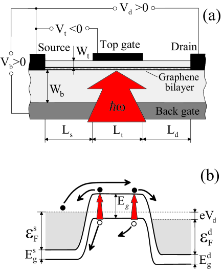
We consider the situation when the gated section is fully depleted. It occurs when , where is the electron charge and are the threshold voltages. The latter correspond to the top-gate voltages at which the bottom of the valence band and the conduction band in the gated section align with the Fermi level in the source section (). The energy gaps in the source, gated, and drain regions, , , and , as well as threshold voltages are given by
| (1) |
| (2) |
where is the electron charge, is the spacing between the graphene layers in the GBL, is the thickness of the layers separating the GBL and the gates (which are assumed to be equal to each other: ), is the Bohr radius, is the dielectric constant, is the effective mass of electrons and holes in the GBL, and is the Planck constant. The parameters and are assumed to be small. For simplicity, we shall neglect some difference between and the efficient spacing which accounts for the effects of electron screening of the transverse electric field between the graphene layer 10 ; 11 .
Considering that electrons in the source and drain sections form 2DEGs (generally with different densities), the Fermi energies in these sections can be presented as
| (3) |
where is the Boltzmann constant and is the temperature. In particular, at sufficiently high back-gate voltages, namely at , one obtains and . One can see that . The latter value is rather small in the case of gate layers made of SiO2 and is very small in the case of gate layers with elevated dielectric constant (say, HfO2).
III Dark current
The source-drain current created by the electrons injected from the source and drain section into the gated section is given by
| (4) |
Here and are the heights of the potential barriers for electrons from the source and drain sides, respectively, and
| (5) |
The factor is the fraction of the injected electrons passed through the gated section despite their scattering on impurities and acoustic phonons. Solving the 2D kinetic Boltzmann equation for the electron distribution function in this section, one can obtain in the ballistic regime of the electron transport across the gated section ( or ), and in the collision-dominated regime (), where is the effective ballistic transit time across the gated section of electrons with the thermal velocity , and is the length of the top gate 15 .
In the dark conditions, and with
| (6) |
Using Eqs. (3), (4), and (6), we arrive at the following formula for the dark current:
| (7) |

Figure 2 shows the dependence of the dark current on the back-gate voltage provided that the top-gate voltage is maintained to be . This corresponds to the highest barrier in the gated section at which the interband tunneling can still be neglected, in particular, owing to a small density of thermal holes in this section. It is assumed that nm, nm, nm, , and . Nonmonotonic behavior of the dark current-voltage characteristics shown in Fig. 2 can be attributed to the interplay of an increase of electron density in the source (drain) section with increasing and an increase in the height of the potential barrier in the gated section when both and simultaneously increase.
IV Photocurrent and responsivity
As a result of illumination with the photon energy , the photogenerated holes are accumulated in the gated section. Their density can be found from the following equation governing the balance between the photogeneration of holes and their escape to the source and drain sections:
| (8) |
Here is the fraction of the holes injected from the gated section into the source and drain sections (i.e., into the contact sections) but not reflected back owing to the scattering ( is determined not only by the hole collision frequency in these section but also by the rate of recombination in these sections and the contacts), , and is the rate of photogeneration of electrons and holes owing to the absorption of the incident THz/IR radiation. This quantity depends on the intensity of radiation , the absorption quantum efficiencies , , and in the pertinent sections, and their lengths. The absorption quantum efficiencies in question are given by 16
| (9) |
| (10) |
where is the speed of light, eV is the band parameter, 12 and is the unity step function reflecting the energy dependence of the density of states near the fundamental edge of absorption. To take into account some smearing of this edge, we set . The factor in Eq. (10) reflects the Burstein-Moss effect 17 :
For the THz/FIR radiation with , Eq. (9) yields . However, the absorption coefficient in the source and drain section can be rather small due to the Burstein-Moss effect. This occurs if the 2D electron gas in these sections is degenerate () and the photon energy does not markedly exceeds the energy gap.. Indeed, at , considering that , from Eq. (10) one obtains . Disregarding therefore the absorption of radiation in the source and drain section and considering that
| (11) |
Eq. (9) can be presented as
| (12) |

The charge of the photogenerated holes in the gated section gives rise to lowering of the potential barrier by the value
| (13) |
Considering Eqs. (4), (7), and (13), the variation of the source-drain current under illumination , i.e., the value of the photocurrent can be presented by the following formula:
| (14) |
It should be noted that the contribution of the photogenerated electrons to the net photocurrent can be neglected because is is small and the photogenerated electrons are swept out from the gated section to both the source and drain section (virtually in equal portions). Then, using Eqs. (7), (11), and (14), we arrive at
| (15) |
Using Eq. (15), the GBL-PT responsivity defined as , where is the net length of the GBL channel (the lengths of the source and drain sections are assumed to be equal to each other:), can be presented
| (16) |
Here, is the collision factor. At meV and , one obtains A/W.
In the most interesting situation when the 2D gases in the source and drain sections are degenerate, the top gate voltage is chosen to provide relatively high barrier for electrons in the source and drain sections, and the source-drain voltage is sufficiently large, i.e., at , , and , Eq. (16) can be reduced to the following:
| (17) |
Here is the photon cut-off energy at which the GBL-PT responsivity reaches a maximum:
| (18) |
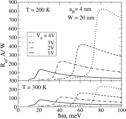
Figure 3 shows the GBL-PT responsivity as a function of the photon energy calculated using Eq. (16) for different back-gate voltages at different temperatures. Here and in the following figures, it is set that for each value of the back-gate voltage the top gate voltage is chosen to be . The source-drain voltage is assumed to be . In such a case, the thermionic dark current is lowered while the interband tunneling is still negligible. We assume that nm, nm, nm, meV, , and . The spectral dependences shown in Fig. 3 correspond to the cut-off photon energies (when ).
Figure 4 shows the dependences of the responsivity maximum value max on the back-gate voltage (and the photon energy ) for the same parameters as in Fig. 3.
V Photoelectric gain and detectivity
Considering Eq. (15) and taking into account that the photocurrent created by the photogenerated electrons and holes as such is equal to , the photoelectric gain can be presented as (compare with Eq. (18))
| (19) |
where all the factors in the right-hand side exceed or greatly exceed unity if ( and 0.07 in the case of SiO2 and HfO2 gate layers, respectively.)
Calculating the GBL-PT dark current limited detectivity as , where is the GBL-PT width (in the direction perpendicular to the current), at properly chosen relationship between and (as above), we arrive at the following formula:
| (20) |
where and . A point worth noting is that the factor in the exponential dependence in Eq. (21) can be about or smaller than unity. Indeed, for nm, one obtains . This provides fairly steep increase in with increasing .


Figures 5 and 6 demonstrate the dark current limited detectivity (under the optimized conditions) as a function of the cut-off photon energy at different temperatures and as a function of at given values . One can see that can be fairly large even at room temperatures. The detectivity markedly decreases with decreasing cut-off photon energy. However, as shown in Fig. 7, in GBL-PTs with relatively high- gate layers in which the Bohr radius can be large, a rather high detectivity can be achieved in the range of low cut-off photon energies, in particular, those corresponding to the THz range of spectrum.
VI Comments
As follows from Eq. (16) - (20) and demonstrated in Figs. 3 - 7, the GBL-PT responsivity and detectivity can be very large even at room temperatures exceeding those of QWIP and QDIPs. This is attributed to the following. First of all, the quantum efficiency of the interband is relatively large (in comparison, say, with the intersubband transitions in single QWIPs). Second, the photoelectric gain exhibited by GBL-PTs can also be very large. This is associated with a higher energy barrier (high activation energy) for the photogenerated holes accumulated in the gated section in comparison with the activation energies for electrons in the source and drain sections. The difference between this activation energies is equal to . An increase in the gate voltages results in an increase of the Fermi energy of electrons in the source and drain section and, in a rise of the activation energy for the photogenerated holes leading to an increase of their lifetime. As a result, the temperature dependence of the GBL-PT detectivity is given by the factor with in contrast to QWIPs (optimized) for which (see, for instance, Refs. 3 ; 5 ). This might open prospects to use GBL-PTs at elevated temperatures.
The GBL-PT responsivity and detectivity can be limited by the interband tunneling of the photogenerated holes if the width of the junction between the source (or drain) section and the gated section is too small ( depends on as well as and ). This can deteriorate the GBL-PT performance due to a decrease in the photoelectric gain associated with a shortening of the lifetime of the photogenerated holes. Estimating the probability of interband tunneling as 18 , where , we arrive at the following condition when the tunneling of the photogenerated holes might be essential:
| (21) |
For instance, for nm, meV, and K, inequality (21) yields nm.
The collision factor in Eqs. (16) - (18) can influence the GBL-PT performance. It depends on the device geometrical parameters and . Since the propagation of holes in the source and drain sections can be strongly affected by scattering on electrons due to their large density, the hole collision frequency in the source and drain sections (or even ). In this case, can exceed unity. This is because strong collisions of holes in the source and drain section can markedly decrease the current of the photogenerated holes from the gated section into the source section (as well as into the drain section) increasing the holes lifetime and, hence, the photoelectric gain. To follow the dependence of (and, consequently, ) on and , assuming that the holes recombine primarily at the contacts, one can use the following interpolation formulas: . and . As a result, we obtain
| (22) |
As follows from Eq. (21), as a function of exhibits a maximum at a certain value of the latter. If both and are large, so that the electron transport in all the sections is collision dominated, .
When the photon energy , the radiation absorption in the source and drain sections can be essential. In such a spectral range, the holes photogenerated in these section can substantially affect the net hole charge in the gated section. In this case, the quantity in the right-hand side of Eq. (8) should be modified to take into account the extra holes photogenerated in the source and drain sections and injected into the gated section. The contribution of the holes photogenerated in the source and drain section can result in a modification in the spectral characteristic of the responsivity at elevated photon energies according to the frequency dependence of the factor in Eq. (10). As a result, a duplicated maxima of can appear which correspond to and .
We considered a GBL-PT with the structure of a single FET. Actually, analogous GBL photodetectors can be made of multiple periodic GBL-PT structures. Such photodetectors can surpass the GBL-PT considered above. However, their operation can be complicated by additional features of the photogenerated holes transport. As a result, the potential distribution along the GBL channel can be nontrivial as it takes place in multiple QWIP (see, for instance, Refs 19 ; 20 ), so that special studies of multiple GBL-PTs are required.
VII Conclusions
We proposed a GBL-PT and calculate its spectral characteristics, dark current, responsivity, and dark current limited detectivity. It was shown that GBL-PTs with optimized structure at properly chosen applied voltages can surpass the photodetectors of other types. The main advantages of GBL-PTs are associated with the utilization of interband transitions with relatively high quantum efficiency, high photoelectric gain, and possibility of operation at elevated temperatures. The advantages of the GBL-PT under consideration in comparison with QWIPs, QDIPs, and QRIPs, as well as with HgCdTe and InSb detectors can also be easy fabrication and integration with silicon (or graphene) readout circuits and the voltage tuning of the spectral characteristics.
Acknowledgments
The authors are grateful to S. Brazovskii, N. Kirova, V. Mitin, V. Aleshkin, T. Otsuji, and E. Sano for useful discussions. The work was supported by the Japan Science and Technology Agency, CREST, Japan.
References
- (1) A. Rogalski, Intersubband Infrared Photodetectors, ed. V. Ryzhii (World Scientific, Singapore, 2003).
- (2) K. K. Choi, The Physics of Quantum Well Infrared Photodetectors (World Scientific, Singapore, 1997)
- (3) H. Schneider and H. C. Liu, Quantum Well Infrared Photodetectors (Springer, Berlin Heidelberg, 2007).
- (4) V. Ryzhii, Semicond. Sci. Technol. 11, 759 (1996).
- (5) V. Ryzhii, I. Khmyrova, M. Ryzhii, and M. Ershov, J. Phys. IV 6, C3-157 (1996).
- (6) C. Berger, Z. Song, T. Li, X. Li, A.Y. Ogbazhi, R. Feng, Z. Dai, A. N. Marchenkov, E. H. Conrad, P. N. First, and W. A. de Heer, J. Phys. Chem. 108, 19912 (2004).
- (7) K. S. Novoselov, A. K. Geim, S. V. Morozov, D. Jiang, M. I. Katsnelson, I. V. Grigorieva, S. V. Dubonos, and A. A. Firsov, Nature 438), 197 (2005).
- (8) B. Obradovic, R. Kotlyar, F. Heinz, P. Matagne, T. Rakshit, M. D. Giles, M. A. Stettler, and D. E. Nikonov, Appl. Phys. Lett. 88, 142102 (2006).
- (9) Z. Chen, Y.-M. Lin, M. J. Rooks, and P. Avouris, Physica E 40, 228 (2007) .
- (10) T. Ohta, A. Bostwick, T. Seyel, K. Horn, and E. Rotenberg, Science 313,951 (2006).
- (11) E. McCann, Phys. Rev. B 74, 161403 (2006).
- (12) E. McCann and V. Fal’ko, Phys. Rev. Lett. 96, 086805 (2006).
- (13) E. V. Castro, K. S. Novoselov, S. V.Morozov, N. M. R. Peres, J. M. L. dos Santos, J. Nilsson, F. Guinea, A. K. Geim, and A. H. Castro Neto, Phys. Rev. Lett. 99, 216802 (2007)
- (14) V. Ryzhii, V. Mitin, M. Ryzhii, N. Ryabova, and T. Otsuji: Appl. Phys. Express 1 (2008) 063002.
- (15) V. Ryzhii, M. Ryzhii, A. Satou, T. Otsuji, and N. Kirova, arXiv:0812.4490 [cond-mat.mes-hall] (2008).
- (16) V. Ya. Aleshkin, A. A. Dubinov, and V. Ryzhii, JETP Lett., 89, No. 2 (2009).
- (17) J. I. Pankove, Optical Processes in Semiconductors (Dover Publications, New York, 1971).
- (18) S. M. Sze, Physics of Semiconductor Devices (Wiley, New York, 1981).
- (19) V. Ryzhii and H. C. Liu, Jpn. J. Appl. Phys. 38, 5815 (1999).
- (20) V. Ryzhii, M. Ryzhii, and H. C. Liu, J. Appl. Phys. 91, 5887 (2002)