10.1080/0010751YYxxxxxxxx \issn1366-5812 \issnp0010-7514
Optical antennas and plasmonics
Abstract
Optical antenna is a nanoscale miniaturization of radio or microwave antennas that is also governed by the rule of plasmonics. We introduce various types of optical antenna and make an overview of recent developments in optical antenna research. The role of local and surface plasmons in optical antenna is explained through antenna resonance and resonance conditions for specific metal structures are explicitly obtained. Strong electric field is shown to exist within a highly localized region of optical antennas such as antenna feed gap or apertures. We describe physical properties of field enhancement in apertures(circular and rectangular holes) and gaps(infinite slit and feed gap), as well as experimental techniques measuring enhanced electric vector field. We discuss about analogies and differences between conventional and optical antennas with a projection of future developments.
keywords:
optical antenna; subwavelength; resonance; surface plasmon; enhancement; metal1 Introduction
Antennas are ubiquitous in modern day communications and come in various forms. In early days, from the Marconi’s first field
test of antennas until World War II, most antennas were of wire type which was used to transmit or receive radio waves.
Developments of microwave technology during and after the War introduced new types of antenna (apertures, microstrips,
phased-array radars, etc.)[1] and shrunk the size of antenna as size depends on the wavelength of an electromagnetic wave.
In the simplest form, antenna is a quarter wavelength long metal pole mounted on a conducting plate
which is known as the monopole antenna.
The typical size of antennas for radio or microwave communications ranges from hundred meters to a few milimeters.
The shift of interest to the higher frequency band of electromagnetic waves in communication, undoubtably optical fiber communication is
one good example, and the advance in nanotechnology and optical science raise one natural question -
is it possible to make “optical antennas”?
At optical frequencies, according to the quarter wavelength resonance condition, the size of antenna may be only about hundred nanometers !
But can we simply shrink down the antenna in proportion to the wavelength to make optical antennas work? In optical fiber
communication, waves are already guided by a fiber and there seems to be no need for antennas which are used for wireless communications.
On the other hand, in wireless optical communication, optical components such as mirror and lens are used to receive optical signals
instead of subwavelength optical antennas as we can see in the case of a telescope.
Then, what can we really do with optical antennas ?
During the past decade, there has been a surge of research activity on the optical properties of metal nanoparticles and metals
with structures at the nanometer scale. The advances in fabrication technique enabled construction of metallic nano structures in various forms.
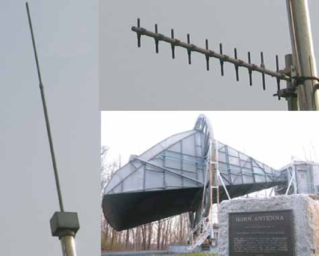
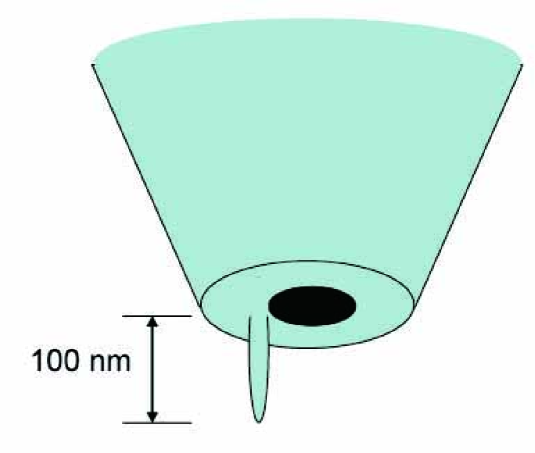
In particular, an optical analogue of monopole antenna - a metal pole of length about 100 nm mounted on a nearfield scanning
optical microscopy(NSOM) tip as illustrated in Fig. 2b has been constructed [2, 3, 4, 5, 6].
Antenna resonance and field localization near an optical monopole antenna have been demonstrated by using single fluorescent
molecules [4]. These efforts begun with a realization that an optical antenna can be used to increase the efficiency
of a near-field optical probe that has a spatial resolution well below the diffraction limit [7].
The subwavelength resolution below the diffraction limit was made possible through the invention of the metal coated, tapered fiber
probe with an aperture of size much smaller than wavelength [8, 9, 10]. Subwavelength size apertures, however, suffer
from a poor coupling efficiency of nearby light since it is known that the coupling efficiency scales as ,
where is the diameter of a hole and is wavelength.
Optical antennas can increase the coupling efficiency by focusing light onto an aperture region.
Another important antenna type is a dipole antenna which is made of two monopole rods separated by a small
gap. The conducting plate of a monopole antenna provides the image of a monopole rod and subsequently
the monopole antenna is in fact equivalent to the dipole antenna. Optical dipole antennas have been used widely
for nearfield optical probes. On resonance, strong field enhancement in the dipole antenna gap
was observed with nanometer-scale gold dipole antennas [11, 12]. Similar enhancement was also obtained
with a nanometer-scale bowtie antenna [13]. Bowtie antenna, a variant of dipole antenna made of two triangle shaped metal pieces,
has been used widely for an optical antenna [7, 13, 14, 15, 16, 17, 18, 19, 20, 21].
Strong electric field with an enhancement factor several orders of magnitude can modify the emission of light by a molecule.
Increased fluorescence of molecules near optical antennas has been reported [4, 22, 23, 24, 25, 26].
Moreover, spectroscopic techniques such as surface-enhanced Raman scattering(SERS) [27], in the presence of a highly localized
strong electric field, allowed optical detection and spectroscopy of a single molecule [28, 29, 30, 31, 32, 33].
Single molecule detection has been also demonstrated using local fields resonantly enhanced by monopole antennas mounted
on a NSOM tip [4, 5, 6] and applied to biological nano-imaging [3, 34].
In this regard, optical antenna is more of a probe for the communication with the nanoscopic world than being a tool for
human-to-human communications.
The enhancement of electric field in an optical dipole antenna is caused essentially by two factors: surface charge and resonance.
Current on an antenna surface which is induced by an incoming light charges the feed gap of a dipole antenna and subsequently establishes
a strong electric field in the gap. Gap charging becomes resonantly enhanced when the antenna geometry meets the resonance condition;
that is, the length of a dipole antenna is an integer multiple of half wavelength. The resonance condition, which holds
for radio and microwave antennas, does not apply directly to optical antennas.
Metal nanorods or wires excited by light show resonance characteristics which are different from the perfectly conducting
case [35, 36, 37, 38, 39, 40, 41, 42, 43].
At optical frequencies, metal is a highly dispersive material with finite conductivity. Electron gas in a
metal can couple to light in the form of a propagating surface wave also called surface plasmon polariton(SPP)[44, 45]
or local plasmons in the case of nanoparticles [46].
Plasmons, either SPP or local plasmons, exhibit salient resonance features. Due to the excitation of local plasmons, the optical properties
of metal nanoparticles for instance are determined by the shape, size and dielectric environment of a metal particle [46].
Recent development of nanofabrication techniques enabled construction of a variety of metal structures at the subwavelength scale
and opened the research area called “plasmonics”, a subfield of nanophotonics studying the manipulation of light coupled to electrons
at the nanoscale [47, 48, 49]. The dispersion relation of SPP and the local plasmon resonance complicate
the resonance feature of optical antennas and modify significantly other features of a conventional antenna.
Roughly speaking, one can not simply shrink down a radio antenna to make an optical antenna.
The properties of optical antennas are still under the intensive study. We may say that research efforts to relate plasmonics
with subwavelength optical antenna have just begun.
The slot antenna is a complementary structure of a dipole antenna formed by cutting a narrow slot in a large piece of metal plate.
The Babinet’s principle suggests that the slot antenna works equally well as its complementary dipole and
various shapes of an aperture can be applied to make optical antennas.
The transmission of electromagnetic wave through a subwavelength size hole is an old subject dating back to
World War II [51, 52], but an optics version of the problem with a new element, plasmon, has ignited
an explosive interest [53, 50] which eventually led to the birth of plasmonics.
Rigorous studies have been made on the transmission of light through a single circular hole
[54, 55, 56, 57, 58, 59, 60, 61, 62] or
other types of apertures such as C-shape [63, 64, 65, 66].
Bowtie shape aperture antennas have received much attention in terms of their capability to gain the strong field confinement and
enhancement [67, 68, 69, 70, 16]. Retangular shape aperture is of particular interest
since it is the geometrical shape of a slot antenna. Half wavelength resonance condition applies to the slot antenna of high conductivity
and a half wave slot leads to a resonantly enhanced and aperture confined electric field [71, 72].
Aperture type optical antennas have the advantage of light confinement and better control of the radiation pattern
compared to the wire type. This initiated efforts on using bowtie aperture antennas to achieve better subwavelength resolution in near
field imaging or nanoscale lithography [68, 69, 70].
The efficiency of a single optical antenna is generally low and the functionality is limited. Modern microwave antenna technology
created various alternatives to overcome these difficulties including phased-array antenna, reflector antenna, frequency-indendent antenna
and microstrip antenna. These alternatives can be also applied to improve optical antennas. The celebrated enhanced transmission
through a periodic array of holes [53] may be attributed to the action of a phased-array optical antenna [73].
Surrounding a single hole by periodic corrugations, so called the Bull’s eye structure, it was demonstrated that the optical aperture antenna
has ability to increase and selectively transmit light with a controlled directivity [74, 75, 76].
The idea of Yagi-Uda antenna [77], which is a directional antenna using reflectors, has been applied in the optical domain
to obtain a directed emission of single emitters and shape light beams [78, 79, 80]. Optical nanostrip antennas have been
studied with an analysis on the slow-plasmon resonance [81, 82].
Optical antennas also open a new realm of application that was not conceived in microwave antennas.
By integrating a resonant optical antenna made of a pair of gold nanorods on the facet of a diode
laser (or a midinfrared quantum cascade laser), a plasmonic laser antenna (or respectively a plasmonic quantum cascade
laser antenna) has been constructed with the ability to confine infrared radiation well below 100 nm [83, 84].
An array of bowtie antennas was proposed as a new tool to produce coherent extreme ultraviolet light [85]. High harmonic generation
was obtained by focusing a femtosecond laser onto a gas inside the bowtie antenna gap.
These efforts demonstrate the exciting potential of optical antennas as a mean of realizing active or nonlinear optical processes
at the nanoscale.
Recent advances in optical antenna theory and application are mostly based on one particular property of an antenna, that is the strong field enhancement at the nano scale region. Plasmonic resonances add a new twist to the problem of antenna resonance and field enhancement. As optical antenna is in a rapidly developing stage, in the present paper we will avoid reviewing optical antennas in detail but will focus on the basic issues of plasmonic resonance and field enhancement which are critical elements of optical antennas. The paper is organized as follows; section 2 introduces antenna resonance and plasmonic resonances existing in optical antennas. Plasmon resonance conditions are explained for various metal geometries: flat surface, cylindrical surface and nanoparticles. Section 3 describes the strong field enhancement in optical aperture type antennas. We explain both resonant and non-resonant field enhancements existing in holes and slit, and introduce vector field mapping techniques. Finally, in Section 4, we discuss about analogies and differences between optical antennas and conventional antennas with a projection of future developments.
2 Antenna resonance and plasmonics
2.1 Monopole antenna
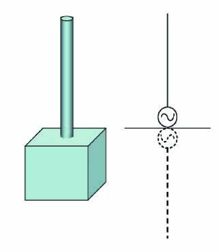
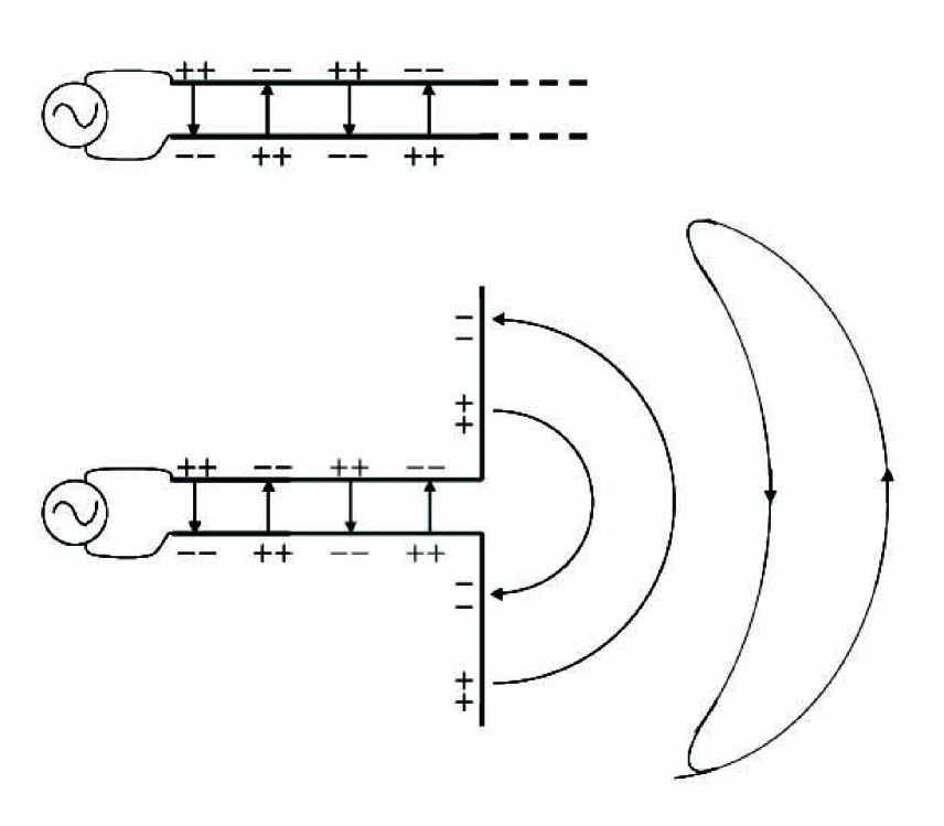
The word antenna as we know was first used by Guglielmo Marconi during his experiment on a wireless transmission using a metal pole (antenna in Italian means pole). A metal pole mounted on a ground or a conducting box is known as a monopole antenna. Marconi’s monopole antennas receive or transmit radio waves most efficiently when the pole is one quarter wavelength in length. To understand this, we first recall the radiation mechanism of a wire antenna. When free electrons on a conducting wire surface are set in motion by the external source, current flows along the surface of a wire. Electrons are accelerated or decelerated if the the driving source is time harmonic, or if the wire geometry blocks constant flow of electrons and these accelerated (decelerated) charges, or equivalently time varying currents, create radiation. To see this more clearly, consider two parallel wires as in Fig. 3a driven by an alternating current source. When two wires are close, electric field lines, emanating from the positive charges on one wire and ending at the negative charges on the other wire, are mostly confined within the region between two wires creating little radiation. If two wires are bent in opposite directions with open ends as in Fig. 3a, electric field lines becomes circularly distorted. As the traveling current reach to the end, field lines become pinched and form a closed loop and finally leave the wire. This wire configuration is called dipole antenna and the radiation pattern is indeed that of a dipole in Fig. 3b. The traveling wave current gets reflected at the end of wire and the reflected wave, when combined with the incident wave, forms a standing wave current pattern with period . Thus, if the total length of the bending section of wires are integer multiple of , the dipole antenna gets resonantly excited increasing the antenna efficiency. A monopole antenna can be thought of a dipole antenna where one half of a dipole antenna is replaced with a ground plane at right-angles to the remaining half. The ground plane, when sufficiently large, provides a reflection forming a mirror image of an antenna as indicated in Fig. 2a. This explains that the resonance length of a monopole antenna is the integer multiple of .
2.2 surface plasmon polaritons
In finding the resonant condition of a monopole antenna, we assumed that the traveling wave current moves at the speed of light and stated that resonance arises when the length is an integer multiple of . Can this be true for any value of , especially for optical wavelengths ? Recent experiment shows that about 80 tall optical monopole antenna is resonant with green light with wavelength of [4]. Obviously, the -rule does not work. Then, what decides the resonance condition ?
Free space Maxwell’s equation is known to be invariant under the scale transformation:
| (1) |
for some constant . In other words, if fields and are given solutions of the wave equation,
| (2) |
we have that and are also solutions. If the scale invariance also works for a monopole antenna, the -resonance condition would hold irrespective of . Scale invariance, however, breaks down in the presence of a dispersive matter such as metal. The dielectric function of a metal is frequency dependent as evidenced in the Drude model of the dielectric function,
| (3) |
where is the volume plasma frequency and is a damping constant. The effect of dispersive dielectric function on the traveling wave current may be best understood in terms of surface plasmons on a flat metal surface.
Surface plasmon polariton(SPP) is a surface electromagnetic wave that propagates in a direction parallel to the metal surface. Consider the metal/dielectric interface at (metal part ) and a surface electromagnetic wave of the form,
| (4) | |||||
where the subscript denotes metal. The wavevector components satisfy
| (5) |
Requiring the continuity of tangential components and at the interface , we have
| (6) |
From the Maxwell’s equation , we find the relation
| (7) |
which together with equation (6) leads to
| (8) |
Combining equations (5) and (8), we finally obtain the dispersion relation
| (9) |
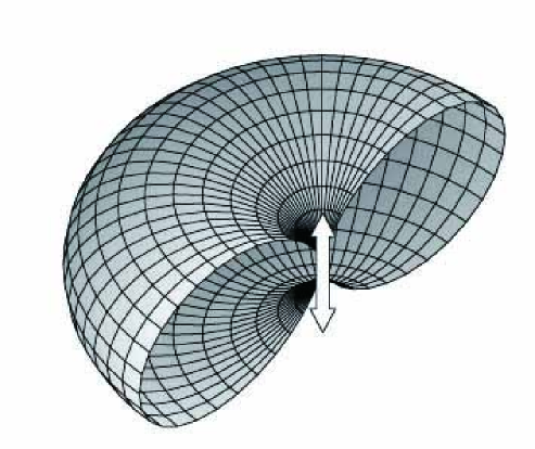
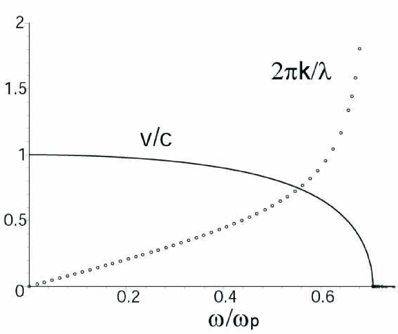
where the choice of sign in taking the square root is made in the following way; we assume for simplicity that the damping coefficient of the dielectric function in (3) is negligibly small so that it may be neglected. We also restrict to the angular frequency smaller than the plasmon frequency . Then, and are negative and quantities inside the square root are all positive. We have chosen positive sign for and which presents a physically sensible solution localized near . As illustrated in Fig. 4a, imaginary and make field decay exponentially as we move away from the interface so that field is localized near . In contrast, is real. This means that field propagates along the surface with velocity and effective wavelength ,
| (10) |
This surface bound electromagnetic wave is the well-known surface plasmon polariton. The dispersion relation and the phase velocity of SPP are given in Fig. 4b.
The divergence free condition of electric field requires that
| (11) |
which implies that both are nonvanishing for a metal having finite conductivity. This in turn implies that there exists nonzero surface charge density . Thus SPP accompanies collective charge oscillations driven by light. Note that for a highly conducting metal, is large and becomes negligibly small so that the localization is very weak. Therefore, in the perfectly conducting limit, SPP ceases to exist if the surface is an infinite plane. Fig. 4b shows that the velocity of SPP decreases as frequency increases. In fact, it reaches to zero at the critical frequency ,
| (12) |
The effective wavelength also shrinks as frequency increases towards . This brings a hope that we could possibly use to explain the discrepancy between the resonance length of a monopole antenna and the quarter wavelength (). In other words, can we expect that ? To check this, we evaluate for an aluminium metal plane. The dielectric constant of aluminium at wavelength 514 nm is , obtained by fitting the Drude model to experimental data [86]. Then, Eq. (10) results in . Though this value smaller than the free space wavelength , it is not sufficiently small to account for the experimentally observed resonance length . One reason for this discrepancy is that we considered surface traveling waves on a flat metal surface while the monopole antenna is made of a rod with diameter smaller than wavelength.
2.3 Cylindrical surface waves
In order to take into account of the shape effect, we need to find travelling waves along the surface of a cylinder having radius . In cylindrical coordinates, field components inside and outside of a cylinder can be written as
| (13) | |||||
where and are undetermined coefficients. and are cylindrical Bessel functions of the first kind and cylindrical Hankel functions of the second kind respectively. Requiring the continuity of fields at leads to
| (14) |
Nonvanishing coefficients exist when the determinant of matrix vanishes,
| (15) |
The zeros of represent the symmetric TM modes of the lossy dielectric cylinder. If we denote the root corresponding to the principle mode by , wavenumber determines the phase velocity of a surface wave by
| (16) |
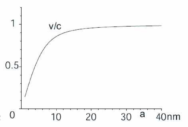
Once again, this exhibits a plasmonic effect through a surface wave propagating along a cylinder with reduced phase velocity. Fig. 5 shows TM mode profiles and the phase velocity of the principle mode as a function of radius. It shows that the phase velocity and subsequently the effective wavelength decreases as the radius becomes smaller. When , . Though shorter than the flat space surface plasmon wavelength, the quarter of is still bigger than the resonance length . The actual monopole antenna, however, is not an infinite cylinder but has a rod end. It was pointed that the reactance of the rod end would increase the antenna length effectively [36] and this modifies the effective wavelength approximately by
| (17) |
One might think as well that the reflection of a surface wave at the rod end suffers a certain amount of phase shift which would increase the antenna length effectively. There could be also experimental factors contributing to the discrepancy for the measured resonance length such as non perfectly conducting ground which however are not our concern. Instead of pursuing a specific monopole antenna problem more(for further details, see for example [37]), we consider the effect of finite size on plasmonic resonances in another well known system - metal nanoparticles.
2.4 Local plasmon resonance and nanoparticles
When small metallic particles are irradiated by light, the conduction electrons oscillate collectively with oscillation frequencies determined by the density and the effective mass of electrons as well as the shape and the size of a metal particle. The density and the effective mass of electrons determine the macroscopic dielectric function in Eq. (3) through the bulk plasma frequency . To relate the shape and the material property to the oscillation frequencies, we consider a simple case of a small spherical metal particle for which the quasi-static approximation is available. If the radius is much smaller than the wavelength , all electrons in a sphere can be assumed to respond simultaneously to electric field of incoming light. In a short time scale, compared to the time period of light, electric field remains to be constant and the interaction can be treated as an electrostatic problem of solving the Laplace equation. Denoting the constant electric field by , the electric field outside the sphere can be readily calculated by solving the potential problem. Take the potential of the form,
| (18) |
The continuity of the tangential electric fields, , and the normal components of the electric displacements, , at the surface of a sphere lead to
| (19) |
Then, the electric field outside the sphere is written as
| (20) |
where and denote dielectric constants of metal and surrounding material respectively. Apart from the incident field, this is the electric field of an induced dipole with the particle polarizability
| (21) |
At first sight, this quasi-static approximation looks to be really static and thus it can not explain the resonance frequency which is a dynamical quantity. The dielectric constant of metal is, however, strongly dependent on frequency. A more rigorous solution of Maxwell equation without the electrostatic approximation shows that the dipole field in (20) is a radiating dipole and the scattering efficiency is proportional to . The plasmon resonance in scattering occurs when the real part of the denominator vanishes such that
| (22) |
Or, if we neglect the damping coefficient , when the dipole plasmon resonance frequency is
| (23) |
Comparison of with the surface plasmon resonance frequency in (12) shows the dependence of ersonance frequency on the shape. A similar dependence can be found for more general shapes. For an ellipsoidal metal particle with principal axes and , the particle polarizability can be found in terms of geometrical depolarization factors along the principal axes [87, 88],
| (24) |
and the dipole plasmon resonance frequency becomes
| (25) |
This reduces to (23) for a spherical case for which . Note that the dipole plasmon resonance frequency in (23) does not depend on the particle size . This is due to the quasi-static approximation which is valid only for particles much smaller than wavelength. For larger particles, the dipole plasmon resonance frequency redshifts due to retardation effects [89] and radiation damping effects [90]. Retardation effects arise since the conduction electrons in a large particle do not move simultaneously in phase and this leads to a reduction of depolarization field. Radiation damping contributes to the plasmon damping resulting the broadenng of resonance spectrum. Retardation and radiation damping effects appear as the lowest-order corrections to the quasi-static approximation. In particular, the dipole plasmon resonance frequency is corrected by
| (26) |
In addition to the dipole, for larger particles there are contributions from higher-order modes (quadrupole, octopole, etc.) and the spectral response is also modified by the higher-order effects. All these corrections can be calculated from the Mie theory of scattering [91].
3 Field enhancement and optical aperture antennas
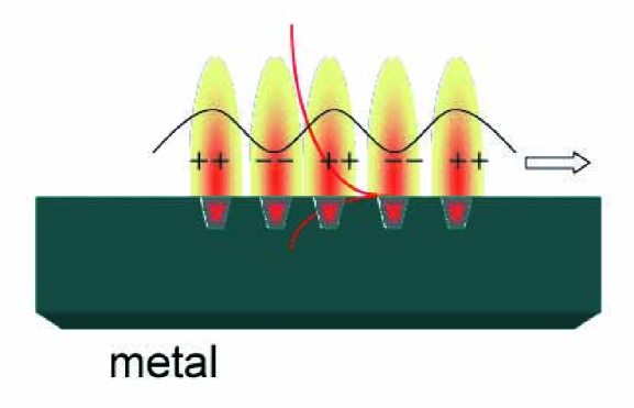
Most antennas were of wire type (monopoles, dipoles, helices etc.) before World War II. During the War, new antenna technology was launched and aperture type antennas(slits, slots, waveguides, horns, reflectors) operating at microwave frequencies were introduced. Aperture type antennas are particularly important in optical applications. Optical bowtie slot antenna is one good example of aperture type antenna that has a better control of the radiation pattern compared to wire antennas. In fact, the uprise of plasmonics has begun with the measurement of extraordinary transmission of light through periodic arrays of holes in an opaque metal film [53]. The role of surface plasmon polaritons in periodic arrays of holes or slits has received much attention [92, 93, 94, 95]. After all, periodic array of holes are nothing but a phased-array optical slot antenna.
3.1 Circular and rectangular holes
How does light pass through a hole of size smaller than or comparable to wavelength? This is a well known question in diffraction theory treated in optics texts books. Fraunhofer diffraction provides far field configurations by utilizing the Huygens-Fresnel principle stating that light splits into outgoing spherical waves when passed through a hole or a slit. When a hole is perforated in a metal, other important contribution arises. Impinging light drives surface current and accumulates charge at the edges of the hole. Accumulated charge in turn enhances electric field inside the hole and subsequently the far field diffracted light. Therefore a metallic aperture can focus and transmit electromagnetic waves with increased efficiency. In other words, it acts as an antenna. This problem was first considered by Bethe in the advancement of microwave technology during the World War II. Bethe developed his theory of light diffraction by idealizing the structure as the circular aperture in a perfectly conducting screen of zero thickness. The transmission efficiency, defiend as transmission cross section divided by hole area, was obtained by Bethe in the long wavelength limit and corrected later to include higher-order terms by Bouwkamp [52]. It is given by
| (27) |
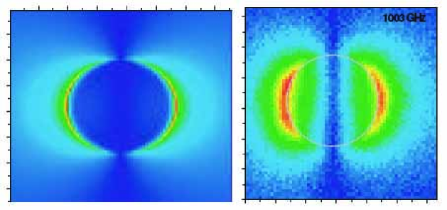
where is the wavenumber of incoming wave and is the radius of a hole. It shows that the transmission efficiency scales as for and drops quickly as becomes small. In the optical application of aperture antennas, focusing light and increasing transmission are important issues while in the microwave application, radiation pattern and directivity of waves are important issues. According to Bouwkamp, the near field -component of electric field at the shadow side (), or the surface charge per permittivity, is written as
| (28) |
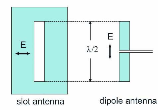
where is the radial coordinate, is the azimuthal angle, and is the amplitude of incoming electric field. The angular -dependence is a characteristic of a dipole emission pattern. This is verified both experimentally and numerically using the Finite Difference Time Domain(FDTD) method as shown in Fig. 6. Indeed, Babinet’s principle relates an aperture antenna with a dipole antenna of wire type. Babinet’s principle states that when a field behind a perfectly conducting screen with an aperture is added to the field of a complementary structure which is obtained by replacing aperture by screen and screen by aperture, then the sum is equal to the field where there is no screen. More rigorously, the (vectorial) Babinet’s principle states that the diffracted electromagnetic fields caused by a screen with apertures and the source field are identical to those of a complementary structure excited by the source field with opposite polarization characteristics . In particular, this implies that the radiation pattern from a circular hole is the same as that of a circular disk with its driving electric field having an opposite polarization. Since circular disk exhibits resonant behavior, we expect that resonance also arises as the size of hole becomes comparable to wavelength . In order to understand the resonance in aperture antennas, we will consider a simpler case of slot antenna, having a rectangular shape aperture.
Consider a TM polarized plane wave impinging normally on a perfectly conducting screen with a rectangular hole. The size of a rectangular hole is , the thickness of screen is , and the amplitude of incoming electric field is . The lowest TE01 mode of electric field inside the hole, directed along the -axis, has the form
| (29) |
For simplicity, we make the single mode approximation such that the electric field inside the hole is governed by the lowest TE01 mode only. Matching tangential components of electric and magnetic fields at the opening and the ending interfaces of hole and also imposing the boundary condition of vanishing tangential electric field on a perfect conductor, one can readily determine the coefficients and so that
| (30) |
where . representing the coupling between incoming wave and the TE01 mode is given by
| (31) |
When the hole is of subwavelength scale (), is approximately equal to . For the screen of nearly zero thickness (), the electric field at the center of the hole is approximately
| (32) |
Now, we are ready to understand the resonance nature of a rectangular aperture. If we assume that the slot is thin () so that is small, Eq. (32) shows that resonance occurs when or the long side of slot is half wavelength long . Note that this is the resonance condition of a dipole antenna of wire type. The direction of electric field is along the -axis which is perpendicular to the long axis of slot. This may be compared with the wire type antenna where the electric field is along the direction of wire. Thus we assured the Babinet’s principle in our case which is illustrated in Fig. 7a. We observe that near resonance electric field is approximately equal to
| (33) |
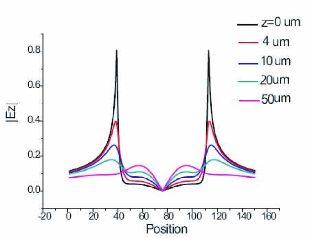
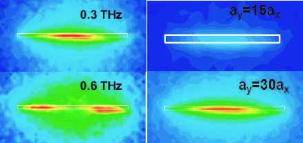
which shows that electric field is inversely proportional to the slot width . Consequently, electric field multiplied by the area of slot remains constant and slot antennas focus electromagnetic field. This focusing property of slot antenna was predicted theoretically [71] and confirmed experimentally using terahertz waves [72]. In Fig. 7b, experimentally measured images of are presented showing resonantly excited fields and the reciprocal dependence on slot width at resonance. When moved away from resonance, the magnitude of enhancement decreases. Nonetheless, enhancement plays an important role as can be seen in the case of an infinitely long slot, that is, slit.
3.2 Field enhancement without resonance: single slit case
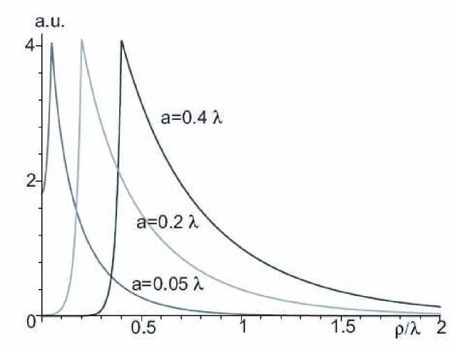
The expression of electric field in a slit may be obtained from Eq. (30) by taking the limit and replacing the TE01 mode by a TEM mode which can be done by changing into a constant. We may fix the constant through matching boundaries as before. The result is written as
| (34) |
where the coupling constant is given by
| (35) |
where is the Euler constant. When the thickness of screen is smaller than wavelength so that , we may approximate by
| (36) |
and additionally if is smaller than the slit width (), can be further approximated to
| (37) |
Once again, this shows that is inversely proportional to and the strong focusing of light is possible even with a non-resonant slit system. Therefore slit also acts as an optical antenna. To understand the physical mechanism of field enhancement, we consider the case where bigger than the slit width () so that is approximately
| (38) |
The meaning of this expression can be understood as follows; recall that an electromagnetic wave reflected on a metal surface induces surface current. On a perfect conductor, the induced surface current is determined by the tangential magnetic field,
| (39) |
where is the unit vector normal to the surface and is the tangential magnetic field just outside the surface. The boundary condition of vanishing tangential electric field requires that for a normally incident plane wave with magnetic field . In the presence of a slit, surface current accumulates charge at the edges of a slit as slit gap blocks the flow of surface current. The induced charge by the surface current can be readily obtained from the charge conservation law:
| (40) |
where is the surface charge density and denotes the two-dimensional divergence. Making integration, we find that the induced charge per unit length can be written as
| (41) |
where is a normal vector to the boundary and the integration is over the unit length of a boundary parallel to slit. We assumed the harmonic time dependence for surface current and charge density . For a narrow gap (), we expect that induced charge resides mostly on the gap surface with surface charge density thereby forming a parallel plate capacitor. Then the resulting electric field,
| (42) |
agrees with that in Eq. (38). This shows that the field enhancement inside a narrow gap indeed results from a capacitative charging of metal edges. We learn from Eq. (37) that for a thin slit ( ), the field enhancement is inversely proportional to the gap size in contrast to a thick slit where it is independent of the gap size. This is rather surprising since it suggest that we can achieve a field enhancement without invoking resonance. Recently, we have demonstrated that, using terahertz waves and a slit of size , the enhancement factor can reach to the value of 800 [96]. The nonresonant enhancement may be attributed to a combined effect of the capacitative charging and the lightning rod effect. A more rigorous account of nonresonant enhancement can be obtained by adopting the “zone” formalism [97].
3.3 Mapping electric and magnetic vecor fields using optical antennas
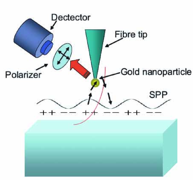
Resonantly excited optical antennas generate strong local variations of electric and magnetic vector fields at the nano scale. Most optical probes detect the intensity of light thus measuring only the magnitude of vector fields. The direction of electric vector field was implicitly captured in the observation of single molecules using NSOM where the orientation of each molecular dipole was determined [98]. The longitudinal electric-field component of Bessel beams was determined by using a polarization sensitive sheet of organic molecule as a probe [99]. Recently, we have shown that the explicit measurement of field vectors, both in magnitude and in direction, is possible [100] when an optical antenna is properly combined with conventional probing techniques. As illustrated in Fig. 8a, we attach a gold nanoparticle at the NSOM fibre tip and place it in the vicinity of nanostructures. Then the local electric field drives the gold particle to act as an oscillating dipole antenna. The radiated field intensity is measured after passing through a rotating polarizer. Since the dipole radiation is critically dependent on the direction of induced dipole, which is in the same direction with driving electric field, the rotating polarizer and subsequently the detection of varying intensity provides information on the electric field vector. In this way, electric field vector maps have been demonstrated [100] but without a full sense of the direction. Since the detection was made on the intensity of light passed through a polarizer, it measures the direction modulo 180 degree.
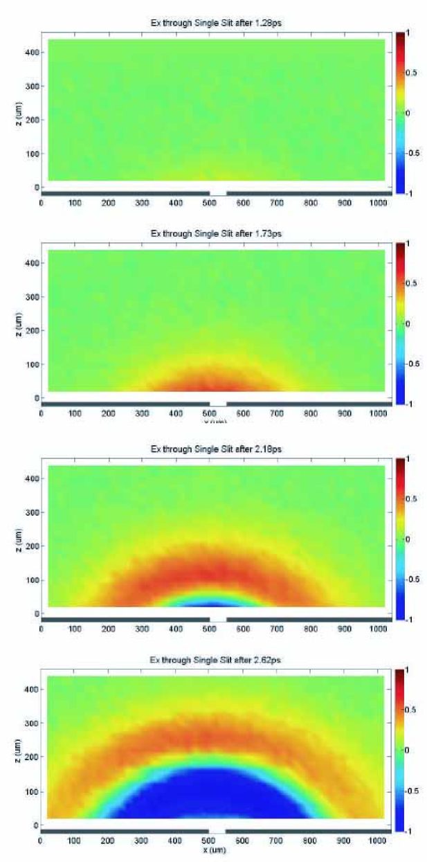
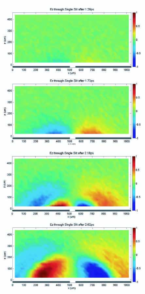
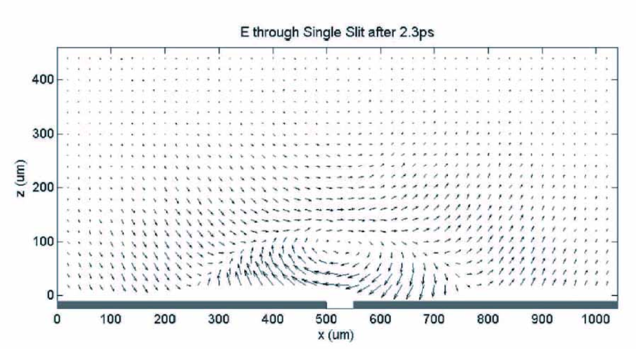
In the terahertz frequency range, this difficulty can be avoided through the terahertz time-domain spectroscopy, which is a spectroscopic technique capable of measuring the phase and amplitude of the electric field in an ultra-wide THz bandwidth [104, 105, 106]. A full vector field map has been obtained using the vectorial Fourier transform two dimensional microscopy [103] which utilizes the advantages of terahertz time domain spectroscopy and the electro-optic sampling technique [107]. In Fig. 9, we show the full electric field vector map of a THz pulse passing through a slit in a metal foil. Time snapshots of the electric field vector components are given in the entire region of space behind the slits, where red and blue colors represent positive and negative values of amplitude. This allows us to draw Faraday field lines of electric field as given in Fig. 10. Moreover, by taking the curl of measured electric field vector, we obtain the time-dependent magnetic field vector, and also the Poynting vector from the knowledge of electric and magnetic fields. In this way, a full vector field map electromagnetic wave has been obtained with a resolution well below wavelength.
4 Discussion
Optical antenna is now becoming a major vehicle for nanophotonics research. As a scaled down version of conventional radio and microwave antennas, optical antenna shares most of common antenna characteristics. Optical analogues of monopole, dipole, directional and phased-array antennas have been constructed and used for various nano-optics applications. We have seen that the resonance condition of antenna changes significantly when we move toward the optical regime. The relatively low conductivity of a metal in the optical domain invokes a collective motion of electrons, i.e. plasmons. Plasmonic resonance is a new element in optical antenna systems. The old geometric resonance such as half wavelength resonance is modified due to the excitation of plasmonic surface waves (surface plasmon polaritons) with shortened wavelengths. The plasmonic resonance, arising in nanoparticles in the form of a dipole plasmon resonance, proves that metal nanoparticle can be an efficient optical antenna. Surface plasmon polaritons do not exist in the ideal case of a perfect conductor and become loosely bound surfaces wave known as Sommerfeld-Zenneck waves[108, 109] for a good conductor such as metal in the THz frequency domain [110, 111]. On the other hand, even for a perfect conductor, it was shown that surface waves can exist if the surface is structured, e.g., with periodic grooves [112]. Structures in a metal surface modifies the dispersion property of surface plasmon polaritons in a controlled way [113, 114]. In antenna applications, grooves on the walls of a horn antenna were used to eliminate the spurious diffractions at the edges of the aperture [115]. Structured surface can be applied to optical antennas as well [74]. The combination of local plasmonic resonance and structural surface plasmon polaritons, which we may simply term as plasmonics, provides ample possibilities for designing optical antennas.
Though we can learn a lot from the analogy between radio antennas and optical antennas, we can make deeper progress from the difference. Since single light photon has much higher energy than a low frequency photon, through field enhancement optical antennas can generate highly energetic local fields. This enables a new realm of applications: active or nonlinear optical processes such as optical antenna lasing and high harmonic generation, or communication with nanoscopic worlds such as single molecules and nanobioimaging [34]. In contrast to the wire type radio antennas, feeding currents though transmission lines and controlling antenna by varying the feed gap are not easy in optical antennas. This makes it difficult to have a circuit theory analysis of optical antenna. Nevertheless, efforts have been made to develop a circuit theory for optical elements at nanoscales [116, 117, 118] and the control of optical antennas have been investigated [120, 121]. Differences will increase as further progresses on optical antenna are being made. Eventually optical antennas, as a beacon and a spear to probe and control nanoworld, will develop into a major field of optics with exciting new discoveries waiting to be found.
Acknowledgement
We thank D. S. Kim for invaluable discussions on the topic and J. H. Eberly for his encouragement. This work is supported in part by KOSEF, KRF, MOCIE and the Seoul R BD program
References
- [1] C. A. Balanis, Antenna Theory: Analyses and Design, John Wiley and Sons, Inc., Hoboken, New Jersey, 2005).
- [2] H. G. Frey, F. Keilmann, A. Kriele, R. Guckenberger, Enhancing the resolution of scanning near-field optical microscopy by a metal tip grown on an aperture probe, Appl. Phys. Lett. 81, 5030 (2002).
- [3] H. G. Frey, S. Witt, K. Felderer, and R. Guckenberger,High-resolution imaging of single fluorescent molecules with the optical near-field of a metal tip, Phys. Rev. Lett. 93, 200801 (2004).
- [4] T. H. Taminiau, R. J. Moerland, F. B. Segerink, L. Kuipers, and N. F. van Hulst, resonance of an optical monopole antenna probed by single molecule fluorescence, Nano Lett. 7, 28 (2007).
- [5] T. H. Taminiau, F. B. Segerink, and N. F. van Hulst, ”A Monopole Antenna at Optical Frequencies: Single- Molecule Near-Field Measurements,” IEEE Trans. Antennas Propag. 55, 3010-3017 (2007).
- [6] T. H. Taminiau, F. B. Segerink, R. J. Moerland, L. Kuipers, and N. F. van Hulst, ”Near-field driving of a optical monopole antenna,” J. Opt. A: Pure Appl. Opt. 9, S315-S321 (2007).
- [7] R. D. Grober, R. J. Schoelkopf, and D. E. Prober, Optical antenna: Towards a unity efficiency near-field optical probe, Appl. Phys. Lett. 70, 1354-1356, (1997).
- [8] A. Lewis, M. Isaacson, A. Harootunian, and A. Murray, Development of a 500 A spatial resolution light microscope. I. Light is efficiently transmitted through diameter apertures, Ultramicroscopy, 13, 227 (1984)
- [9] D.W. Pohl, W. Denk, and M. Lanz, Optical stethoscopy: Image recording with resolution , Appl. Phys. Lett., 44, 651 (1984).
- [10] E. Betzig, J. K. Trautman, T. D. Harris, J. S. Weiner, and R. L. Kostelak, Breaking the Diffraction Barrier: Optical Microscopy on a Nanometric Scale, Science 251, 1468 (1991).
- [11] P. Mühlschlegel, H. J. Eisler, O. J. F. Martin, B. Hecht, and D. W. Pohl, Resonant Optical Antennas, Science 308, 1607 (2005).
- [12] P. Ghenuche, S. Cherukulappurath, T. H. Taminiau, N. F. van Hulst, and R. Quidant, Spectroscopic Mode Mapping of Resonant Plasmon Nanoantennas, Phys. Rev. Lett. 101, 116805 (2008)
- [13] P. J. Schuck, D. P. Fromm, A. Sundaramurthy, G. S. Kino, and W. E. Moerner, Improving the Mismatch between Light and Nanoscale Objects with Gold Bowtie Nanoantennas, Phys. Rev. Lett. 94, 017402 (2005).
- [14] J. N. Farahani, D.W. Pohl, H.-J. Eisler, and B. Hecht Single quantum dot coupled to a scanning optical antenna: a tunable superemitter, Phys. Rev. Lett. 95, 017402 (2005).
- [15] J. N. Farahani, H.-J. Eisler, D.W. Pohl, M. Pavius, P. Flückiger, P. Gasser, and B. Hecht, Bow-tie optical antenna probes for single-emitter scanning near-field optical microscopy, Nanotechnology 18, 125506 (2007).
- [16] H. Guo, T. P. Meyrath, T. Zentgraf, N. Liu, L. Fu, H. Schweizer, and H. Giessen, Optical resonances of bowtie slot antennas and their geometry and material dependence, Opt. Express 16, 7756-7766 (2008).
- [17] H. Fischer and O. J. F. Martin, Engineering the optical response of plasmonic nanoantennas, Opt. Express 16, 9144-9154 (2008).
- [18] C. Huang, A. Bouhelier, G. Colas des Francs, A. Bruyant, A. Guenot, E. Finot, J.-C. Weeber, and A. Dereux Gain, detuning, and radiation patterns of nanoparticle optical antennas, Phys. Rev. B 78, 155407 (2008).
- [19] D. P. Fromm, A. Sundaramurthy, P. J. Schuck, G. Kino, and W. E. Moerner, Gap-Dependent Optical Coupling of Single Bowtie Nanoantennas Resonant in the Visible, Nano Lett. 4, 957-961 (2004).
- [20] L. Wang, S. M. Uppuluri, E. X. Jin, and X. Xu, Nanolithography Using High Transmission Nanoscale Bowtie Apertures, Nano Lett. 6, 361-364 (2006).
- [21] A. Sundaramurthy, P. J. Schuck, N. R. Conley, D. P. Fromm, G. S. Kino, andW. E.Moerner, Toward Nanometer- Scale Optical Photolithography: Utilizing the Near-Field of Bowtie Optical Nanoantennas, Nano Lett. 6, 355-360 (2006).
- [22] S. Kühn, U. Hakanson, L. Rogobete, and V. Sandoghdar, ”Enhancement of Single-Molecule Fluorescence Using a Gold Nanoparticle as an Optical Nanoantenna,” Phys. Rev. Lett. 97, 017402 (2006).
- [23] P. Bharadwaj, P. Anger and L. Novotny, Nanoplasmonic enhancement of single-molecule fluorescence, Nanotechnology 18, 044017 (2007).
- [24] P. Bharadwaj and L. Novotny, Spectral dependence of single molecule fluorescence enhancement, Optics Express 15, 14266-14274 (2007).
- [25] F. Tam, G. P. Goodrich, B. R. Johnson, and N. J. Halas, Plasmonic Enhancement of Molecular Fluorescence, Nano Lett. 7, 496-501 (2007).
- [26] R. M. Bakker, H.-K. Yuan, Z. Liu, V. P. Drachev, A. V. Kildishev, V. M. Shalaev, R. H. Pedersen, S. Gresillon, A. Boltasseva, Enhanced localized fluorescence in plasmonic nanoantennae, Appl. Phys. Lett. 92, 043101 (2008).
- [27] J. Gersten and A. Nitzan, Electromagnetic theory of enhanced Raman scattering by molecules adsorbed on rough surfaces, J. Chem. Phys. 73, 3023-3037 (1980).
- [28] S. Nie, and S. R. Emory, Probing Single Molecules and Single Nanoparticles by Surface-Enhanced Raman Scattering, Science 275, 1102-1106 (1997).
- [29] K. Kneipp, Y. Wang, H. Kneipp, L. T. Perelman, I. Itzkan, R. R. Dasari, and M. S. Feld, Single Molecule Detection Using Surface-Enhanced Raman Scattering (SERS), Phys. Rev. Lett. 78, 1667 (1997).
- [30] H. Xu, E. J. Bjerneld, M. K all, and L. Brjesson, Spectroscopy of Single Hemoglobin Molecules by Surface Enhanced Raman Scattering, Phys. Rev. Lett. 83, 4357 (1999).
- [31] N. Felidj, J. Aubard, G. Levi, J. R. Krenn, A. Hohenau, G. Schider, A. Leitner, and F. R. Aussenegg, Optimized surface-enhanced Raman scattering on gold nanoparticle arrays, Appl. Phys. Lett. 82, 3095-3097 (2003).
- [32] L. Rogobete, F. Kaminski, M. Agio, and V. Sandoghdar, Design of plasmonic nanoantennae for enhancing spontaneous emission, Opt. Lett. 32, 1623-1625 (2007).
- [33] T. H. Taminau, F. D. Stefani, F. B. Segerink and N. F. Van Hulst, Optical antennas direct single-molecule emission, Nature Photonics 2, 234-237 (2008).
- [34] M. F. Garcia-Parajo, Optical antennas focus in on biology, Nature Photon. 2, 201-203 (2008).
- [35] K. Imura, T. Nagahara, and H. Okamoto, Near-field optical imaging of plasmon modes in gold nanorods, J. Chem. Phys. 122, 154701 (2005).
- [36] L. Novotny, Effective wavelength scaling for optical antennas, Phys. Rev. Lett. 98, 266802 (2007).
- [37] G. W. Hanson, On the Applicability of the Surface Impedance Integral Equation for Optical and Near Infrared Copper Dipole Antennas, IEEE Trans. Ant. and Prop., vol 54, 3677-3685 (2006).
- [38] H. Ditlbacher, A. Hohenau, D. Wagner, U. Kreibig, M. Rogers, F. Hofer, F. R. Aussenegg, and J. R. Krenn, Silver Nanowires as Surface Plasmon Resonators, Phys. Rev. Lett. 95, 257403 (2005).
- [39] F. Neubrech et al., Resonances of individual metal nanowires in the infrared, Appl. Phys. Lett. 89, 253104 (2006).
- [40] T. Laroche and C. Girard, Near-field optical properties of single plasmonic nanowires, Appl. Phys. Lett. 89, 233119 (2006).
- [41] E. K. Payne, K. L. Shuford, S. Park, G. C. Schatz, and C. A. Mirkin, Multipole Plasmon Resonances in Gold Nanorods, J. Phys. Chem. B 110, 2150-2154, (2006).
- [42] K. B. Crozier, A. Sundaramurthy, G. S. Kino, and C. F. Quate, Optical antennas: Resonators for local field enhancement, J. Appl. Phys. 94, 4632-4642, (2003).
- [43] G. Schider, J. R. Krenn, A. Hohenau, H. Ditlbacher, A. Leitner, F. R. Aussenegg, W. L. Schaich, I. Puscasu, B. Monacelli, and G. Boreman, Plasmon dispersion relation of Au and Ag nanowires, Phys. Rev. B 68, 155427 (2003).
- [44] R. H. Ritchie, Plasma losses by fast electrons in thin films, Phys. Rev. 106, 874.881 (1957).
- [45] H. Raether, Surface Plasmons on Smooth and Rough Surfaces and on Gratings, Springer, Berlin, (1988).
- [46] K. L. Kelly, E. Coronado, L. L. Zhao, and G. C. Schatz, The Optical Properties of Metal Nanoparticles: The Influence of Size, Shape, and Dielectric Environment, J. Phys. Chem. B 107, 668-677 (2003).
- [47] W. L. Barnes, , A. Dereux, and T. W. Ebbesen, Surface plasmon subwavelength optics, Nature 424, 824.830 (2003).
- [48] S. A. Maier and H. A. Atwater, Plasmonics: Localization and guiding of electromagnetic energy in metal/dielectric structures, J. Appl. Phys. 98, 011101 (2005).
- [49] S. Lal, S. Link, and N. J. Halas, Nano-optics from sensing to waveguiding, Nature Photonics 1, 641-648 (2007).
- [50] C. Genet and T. W. Ebbesen, Light in tiny holes, Nature, 445, 39-46 (2007).
- [51] H. A. Bethe, Theory of diffraction by small holes, Phys. Rev. 66, 163-182 (1944).
- [52] C. J. Bouwkamp, Diffraction theory, Reports on Progress in Physics XVIII, 35 (1954).
- [53] T. W. Ebbesen, H. J. Lezec, H. F. Ghaemi, T. Thio, and P. A. Wolff, Extraordinary optical transmission through sub-wavelength hole arrays, Nature 391, 667-669 (1998).
- [54] A. Degiron, H. J. Lezec, N. Yamamoto, and T. W. Ebbesen, Optical transmission properties of a single subwavelength aperture in a real metal, Optics Commun. 239, 61-66 (2004).
- [55] A. Degiron and T. W. Ebbesen, Analysis of the transmission process through single apertures surrounded by periodic corrugations, Opt. Express 12, 3694-3700 (2004).
- [56] A. R. Zakharian, M. Mansuripur, and J. V. Moloney, Transmission of light through small elliptical apertures, Opt. Express 12, 2631-2648 (2004).
- [57] Y. Alaverdyan, B. Sepulveda, L. Eurenius, E. Olsson, and M. Kall, Optical antennas based on coupled nanoholes in thin metal films, Nature Phys. 3, 884-889 (2007).
- [58] T. Rindzevicius, Y. Alaverdyan, B. Sepulveda, T. Pakizeh, M. Kall, R. Hillenbrand, J. Aizpurua, and F. J. Garcia de Abajo, Nanohole plasmons in optically thin gold films, J. Phys. Chem. C 111, 1207 (2007).
- [59] J. Prikulis, P. Hanarp, L. Olofsson, D. Sutherland, and M. Kall, Optical spectroscopy of nanometric holes in thin gold films, Nano Lett. 4, 1003-1007 (2004).
- [60] B. Sepulveda, Y. Alaverdyan, J. Alegret, M. Kall and P. Johansson, Shape effects in the localized surface plasmon resonance of single nanoholes in thin metal films, Opt. Express 16, 5609-5616 (2008).
- [61] E. Popov, M. Neviere, A. Sentenac, N. Bonod, A.-L. Fehrembach, J. Wenger, P.-F. Lenne, and H. Rigneault, Single-scattering theory of light diffraction by a circular subwavelength aperture in a finitely conducting screen, J. Opt. Soc. Am. A 24, 339-358, (2007).
- [62] F. J. Garcia de Abajo, Light transmission through a single cylindrical hole in a metallic film, Opt. Express 10, 1475-1484 (2002).
- [63] X. Shi, L. Hesselink, and R. L. Thornton, Ultrahigh light transmission through a C-shaped nanoaperture, Opt. Lett. 28, 1320-1322 (2003).
- [64] J. A. Matteo, D. P. Fromm, Y. Yuen, P. J. Schuck, W. E. Moerner, and L. Hesselink, Spectral analysis of strongly enhanced visible light transmission through single C-shaped nanoapertures, Appl. Phys. Lett. 85, 648 (2004).
- [65] L. Sun and L. Hesselink, Low-loss subwavelength metal C-aperture waveguide, Opt. Lett. 31, 3606 (2006).
- [66] J. W. Lee, M. A. Seo, D. J. Park and D. S. Kim, S. C. Jeoung, C. Lienau, Q. H. Park, P. C. M. Planken, Shape resonance omni-directional terahertz filters with near-unity transmittance, Opt. Express 14, 1253-1259 (2006).
- [67] E. X. Jin and X. Xu, Plasmonic effects in near-filed optical transmission enhancement through a single bowtieshaped aperture, Appl. Phys. B. 84, 3 (2006).
- [68] K. Ishihara, K. Ohashi, T. Ikari, H. Minamide, H. Yokoyama, J. Shikata, and H. Ito, Terahertz-wave near-field imaging with subwavelength resolution using surface-wave-assistanted bow-tie aperture, Appl. Phys. Lett. 89, 201120 (2006).
- [69] L. Wang, S. M. Uppuluri, E. X. Jin, and X. Xu, Nanolithography using high transmission nanoscale bowtie apertures, Nano Lett. 6, 361 (2006).
- [70] L.Wang and X. Xu, High transmission nanoscale bowtie-shaped aperture probe for near-field optical imaging, Appl. Phys. Lett. 90, 261105 (2007).
- [71] F. J. Garcia-Vidal, E. Moreno, J. A. Porto, and L. Martin-Moreno, Transmission of Light through a Single Rectangular Hole, Phys. Rev. Lett. 95, 193901 (2005).
- [72] M. A. Seo, A. J. L. Adam, J. H. Kang, J. W. Lee, K. J. Ahn, Q. H. Park, P. C. M. Planken, and D. S. Kim, Near field imaging of terahertz focusing onto rectangular apertures, Opt. Express 16, 20484-20489 (2008).
- [73] Z. J. Zhang, R. W. Peng, Z. Wang, F. Gao, X. R. Huang, W. H. Sun, Q. J. Wang, and Mu Wang, Plasmonic antenna array at optical frequency made by nanoapertures, Appl. Phys. Lett. 93, 171110 (2008).
- [74] H. J. Lezec, A. Degiron, E. Devaux, R. A. Linke, L. Martin-Moreno, F. J. Garcia-Vidal, and T. W. Ebbesen, Beaming light from a subwavelength aperture, Science 297, 820-822 (2002).
- [75] A. Degiron, and T. W. Ebbesen, Analysis of the transmission process through single apertures surrounded by periodic corrugations, Opt. Express 12, 3694-3700 (2004).
- [76] L. Martin-Moreno, F. J. Garcia-Vidal, H. J. Lezec, A. Degiron, and T. W. Ebbesen, Theory of highly directional emission from a single subwavelength aperture surrounded by surface corrugations, Phys. Rev. Lett. 90, 167401 (2003).
- [77] H. Yagi, Beam transmission of ultra short waves, Proc. IRE 16, 715-741 (1928).
- [78] T. H. Taminiau, F. D. Stefani, and N. F. van Hulst, Enhanced directional excitation and emission of single emitters by a nano-optical Yagi-Uda antenna, Opt. Express 16, 10858-10866 (2008).
- [79] J. Li, A. Salandrino, and N. Engheta, Shaping light beams in the nanometer scale: A Yagi-Uda nanoantenna in the optical domain, Phys. Rev. B 76, 245403-245407 (2007).
- [80] H. F. Hofmann, T. Kosako, and Y. Kadoya,Design parameters for a nano-optical Yagi-Uda antenna, New J. Phys. 9, 217-217 (2007).
- [81] T. Sndergaard and S. I. Bozhevolnyi, Slow-plasmon resonant nanostructures: scattering and field enhancements, Phys. Rev. B 75, 073402 (2007).
- [82] T. Sndergaard, J. Beermann, A. Boltasseva, and S. I. Bozhevolnyi, Slow-plasmon resonant-nanostrip antennas: analysis and demonstration, Phys. Rev. B 77, 115420 (2008)
- [83] E. Cubukcu, E. A. Kort, K. B. Crozier, and F. Capasso, Plasmonic laser antenna, Appl. Phys. Lett. 89, 093120 (2006).
- [84] N. Yu, E. Cubukcu, L. Diehl, M. A. Belkin, K. B. Crozier, and F. Capasso, D. Bour, S. Corzine, and G. Hoflerer, Plasmonic quantum cascade laser antenna, Appl. Phys. Lett. 91, 173113 (2007).
- [85] S. Kim, J. Jin, Y.-J. Kim, I.-Y. Park, Y. Kim, and S.-W. Kim, High-harmonic generation by resonant plasmon field enhancement, Nature 453, 757-760, (2008).
- [86] M. J. Weber, Handbook of Optical Materials, CRC Press, London (2003).
- [87] U. Kreibig and M. Vollmer, Optical Properties of Metal Clusters, Springer, Berlin, (1995).
- [88] C. F. Bohren and D. R. Huffman, Absorption and Scattering of Light by Small Particles, Wiley, New York, (1983).
- [89] M. Meier and A. Wokaun, Enhanced fields on large metal particles: dynamic depolarization, Opt. Lett. 8, 581 (1983).
- [90] A. Wokaun, J. P. Gordon, and P. F. Liao, Radiation Damping in Surface- Enhanced Raman Scattering, Phys. Rev. Lett. 48, 957 (1982).
- [91] G. Mie, Ann. Phys. 25, 377 (1908).
- [92] J. A. Porto, F. J. Garcia-Vidal, and J. B. Pendry, Transmission resonances on metallic gratings with very narrow slits, Phys. Rev. Lett. 83, 2845 (1999).
- [93] M. M. J. Treacy, Dynamical diffraction explanation of the anomalous transmission of light through metallic gratings, Phys. Rev. B 66, 195105 (2002).
- [94] Q. Cao and P. Lalanne, Negative role of surface plasmons in the transmission of metallic gratings with very narrow slits, Phys. Rev. Lett. 88, 057403 (2002).
- [95] K. G. Lee, and Q-Han Park, Coupling of surface plasmon polaritions and light in metallic nanoslits, Phys. Rev. Lett. 95, 103902 (2005).
- [96] M. A. Seo et al. Terahertz nanogap device for field enhancement, submitted.
- [97] J. H. Kang, D. S. Kim, and Q. H. Park, Local capacitor model for plasmonic electric field enhancement, submitted.
- [98] E. Betzig and R. J. Chichester, Single molecules observed by near-field scanning optical microscopy, Science 262, 1422-1425 (1993).
- [99] T. Grosjean and D. Courjon, Photopolymers as vectorial sensors of the electric field, Opt. Express 14, 2203-2210 (2006).
- [100] K. G. Lee et al., Vector field microscopic imaging of light, Nature Photon. 1, 53.56 (2007).
- [101] F. Zenhausern,, M. P. O’Boyle, and H. K. Wickramasinghe, Apertureless near-field optical microscope, Appl. Phys. Lett. 65, 1623.1625 (1994).
- [102] S. Kawata and Y. Inouye, Scanning probe optical microscopy using a metallic probe tip, Ultramicroscopy 57, 313.317 (1995).
- [103] M. A. Seo, A. J. L. Adam, J. H. Kang, J. W. Lee, S. C. Jeoung, Q. H. Park, P. C. M. Planken, and D. S. Kim, Fourier-transform terahertz near-field imaging of one-dimensional slit arrays: mapping of electric-field-, magnetic-field-, and Poynting vectors, Opt. Express 15, 11781-11789 (2007).
- [104] M. van Exter and D. R. Grischkowsky, Characterization of an optoelectronic terahertz beam system, IRE Trans. Microwave Theory and Tech. 38, 1684-1691 (1990).
- [105] Q. Wu and X. C. Zhang, Free-space electro-optic sampling of terahertz beams, Appl. Phys. Lett. 67, 3523-3525 (1995).
- [106] G. Zhao, R. N. Schouten, N. van der Valk, W. T. Wenckebach, and P. C. M. Planken, Design and performance of a THz emission and detection setup based on a semi-insulating GaAs emitter, Rev. Sci. Instrum. 73, 1715-1719 (2002).
- [107] G. Gallot and D. R. Grischkowsky, Electro-optic detection of terahertz radiation, J. Opt. Soc. Am. B 16, 1204-1212 (1999).
- [108] A. Sommerfeld, Ann. Phys. U. Chemie 67-1,233, (1899).
- [109] J. Zenneck, Ann. d. Phys. 23, 846, (1907).
- [110] K. Wang and D.M.Mittleman, Metal wires for THz wave guiding, Nature 432, 376 (2004).
- [111] T.I. Jeon, J. Zhang, D. Grischkowsky, THz Sommerfeld wave propagation on a single metal wire, Appl. Phys. Lett. 86, 161904 (2005),
- [112] G. Goubau, Surface waves and their application to transmission lines, J. Appl. Phys. 21, 1119 (1950).
- [113] F. J. Garcia de Abajo, and J. J. Saénz, Electromagnetic Surface Modes in Structured Perfect-Conductor Surfaces, Phys. Rev. Lett. 95, 233901 (2005).
- [114] S. A. Maier, S. R. Andrews, L. Martin-Moreno,and F. J. Garcia-Vidal, Terahertz Surface Plasmon-Polariton Propagation and Focusing on Periodically Corrugated Metal Wires, Phys. Rev. Lett. 97, 176805 (2006).
- [115] A. F. Kay, The scalar feed, AFCRL Rep. 64-347, AD601609, March 1964.
- [116] N. Engheta, Circuits with light at nanoscales: optical nanocircuits inspired by metamaterials Science 317, 1698 (2007);
- [117] N. Engheta, A. Salandrino, and A. Alù, Circuit elements at optical frequencies: nanoinductors, nanocapacitors, and nanoresistors, Phys. Rev. Lett. 95, 095504 (2005)
- [118] A. Alù and N. Engheta, Input impedance, nanocircuit loading, and radiation tuning of optical nanoantennas, Phys. Rev. Lett. 101, 043901 (2008)
- [119] P. J. Burke, S. Li, and Z. Yu, Quantitative Theory of Nanowire and Nanotube Antenna Performance, IEEE Trans. Nanotech. 5, 314-334, (2006)
- [120] J. Merlein et al. Nanomechanical control of an optical antenna, Nature Photon. 2, 230-233 (2008).
- [121] A. Alù and N. Engheta, Tuning the scattering response of optical nanoantennas with nanocircuit loads, Nature Photon. 2, 307-310 (2008).