Linearized SQUID Array (LISA) for High Bandwidth Frequency-Domain Readout Multiplexing
Abstract
We have designed and demonstrated a Superconducting Quantum Interference Device (SQUID) array linearized with cryogenic feedback. To achieve the necessary loop gain a 300 element series array SQUID is constructed from three monolithic 100-element series arrays. A feedback resistor completes the loop from the SQUID output to the input coil. The short feedback path of this Linearized SQUID Array (LISA) allows for a substantially larger flux-locked loop bandwidth as compared to a SQUID flux-locked loop that includes a room temperature amplifier. The bandwidth, linearity, noise performance, and 3 dynamic range of the LISA are sufficient for its use in our target application: the multiplexed readout of transition-edge sensor bolometers.
I Introduction
A new generation of fully lithographed Transition-Edge Sensor (TES) bolometers has been developed for astronomical observations in the far-IR to millimeter wavelength range. These devices allow for large arrays of or more bolometers(Audley et al. (2007); Tran (2007); Grainger et al. (2008); Ruhl et al. (2004); D. Schwan for the APEX-SZ Collaboration (2003)), providing a substantial step forward in sensitivity. A significant challenge for scaling arrays is readout multiplexing. We have developed the superconducting quantum-interference device (SQUID) based frequency-domain readout multiplexer (fMUX) Yoon et al. (2001); Spieler (2002); Lanting et al. (2004); Dobbs et al. (2007). The fMUX is currently deployed on two active experiments Ruhl et al. (2004); D. Schwan for the APEX-SZ Collaboration (2003) and will be used for a number of experiments in the near future Tran (2007); Oxley et al. (2004). A digital implementation of the room temperature components of the fMUX Dobbs et al. (2007) system is being integrated with these experiments. The digital electronics has sufficient capacity to extend the multiplexed channel count. A complementary SQUID-based readout multiplexing technique is time domain multiplexing (Chervenak et al. (1999, 2000); M. Halpern (2007)).
With the fMUX system, the number of detectors that can be instrumented with a single SQUID-based cryogenic amplifier is proportional to the readout bandwidth. For the existing fMUX system, the readout bandwidth of MHz allows multiplexing of 8-16 channels. The readout bandwidth is fundamentally limited by the SQUID feedback electronics which include a stage at room temperature. In this paper we report on the design and performance of the Linearized SQUID Array (LISA) in which the first stage of the feedback electronics is moved to the cryogenic stage. This configuration allows for an increase in readout bandwidth and thus a corresponding increase in the number of multiplexed pixels by more than an order of magnitude.
The LISA provides the cryogenic amplification necessary to increase the channel count of the fMUX system and coupled with the digital room temperature electronics, this device represents a new generation in fMUX technology. Furthermore, because of its simple design that is easily implemented on a single chip, its low power dissipation, and its low input noise current, the LISA is an excellent general purpose cryogenic transimpedance amplifier.
In this paper we describe the design and testing of a prototype LISA, utilizing several (three, in this example) 100-SQUID arrays connected in series with a cryogenic feedback resistor connecting the combined output of the SQUIDs to the input coil. The dynamic range, linearity, and input noise of the LISA meet the fMUX design specifications across a readout bandwidth of 10 MHz.
II Primary Application
Our target application for the LISA is the multiplexed readout of transition edge sensor (TES) bolometer arrays for the detection of mm-wavelength radiation. These cryogenic detectors employ a 3 mm metal absorber that is weakly coupled to a 250 mK thermal bath. Radiation incident on the absorber induces a temperature rise. This temperature change is measured with a TES thermistor coupled to the absorber. The TES thermistor is operated in the transition between its superconducting state and its normal state where a small change in temperature yields a large change in resistance. Large arrays of these TES bolometers can be manufactured photolithographically making possible the new generation of mm-wavelength observations listed above.
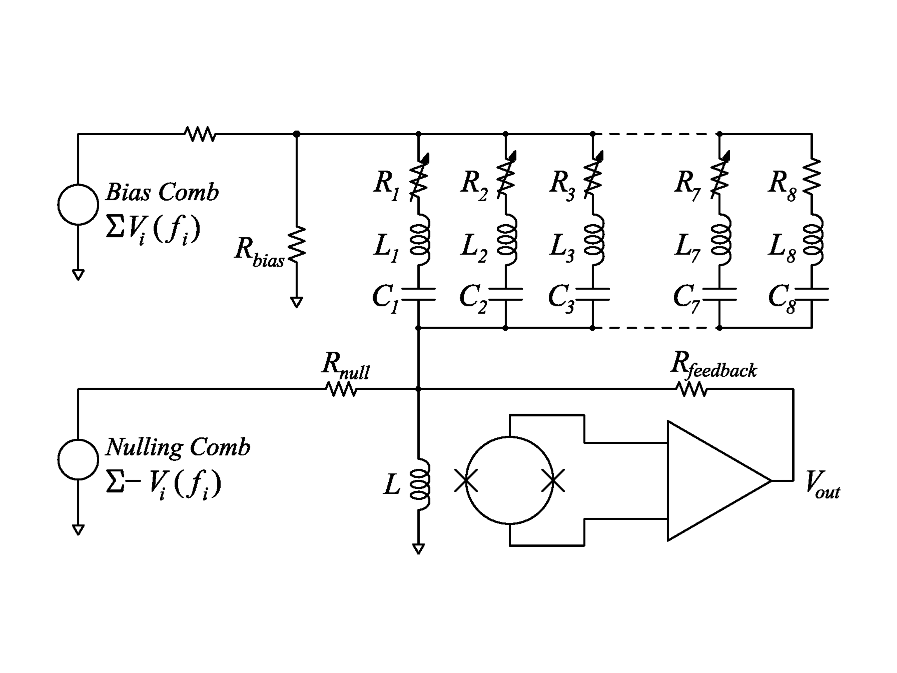
In the fMUX readout system, the TES devices are biased into their superconducting transitions with high-frequency (0.3 – 1 MHz) sinusoidal bias voltages. A change in the incident radiation power induces a change in the TES resistance that amplitude modulates its bias carrier. This translates the signal to sidebands above and below the carrier frequency. Each TES bolometer is biased at a different frequency, so the signals are now uniquely positioned in frequency space and the currents from the individual thermistors can be summed into one wire. The summed currents are fed to the input of a transimpedance amplifier utilizing a DC SQUID operating in a flux-locked loop (FLL) configuration (see Fig. 1). The TES thermistor typically has an impedance of , a noise current of 10-50 pA/, and requires a bias voltage of .
The SQUID electronics performance requirements for this application are: (1) white noise lower than the TES noise ( pA/), (2) sufficient bandwidth( MHz) to accommodate many carriers, (3) input impedance much lower than the TES impedance () across the entire bandwidth to maintain constant-voltage bias, (4) sufficient transimpedance () to override the 1 nV/ noise of a warm amplifier which follows the system, (5) large () dynamic range in order to accommodate a single carrier signal, and (6) sufficient linearity to amplify large carrier signals and to reduce intermodulation between multiple carriers. Low frequency noise in the SQUID electronics is not an issue as the signals of interest have been translated to frequencies above 0.3 MHz.
The dynamic range requirement allows the system to handle at least one full sized carrier. This allows a user to tune the system in a straight forward manner (tuning typically involves choosing the appropriate bias voltage level for a particular sensor). After tuning a single sensor, the carrier is nulled with a 180∘ unmodulated copy of the carrier signal injected at the input coil of the SQUID. This does not affect the original signals, as all of their information is in the sidebands. Once the first carrier is nulled, a second one can be added without increasing the dynamic range requirement. Thus, the number of channels that can be multiplexed with a single set of SQUID electronics is fundamentally limited by the bandwidth of these electronics and not by the dynamic range.
III Linearized SQUID Array
The response of a SQUID has traditionally been linearized with a feedback loop that includes a transistor amplifier operating at 300K. The bandwidth of this flux-locked loop circuit is limited by propagation delays along the wires connecting this amplifier to the SQUID which operates at the cold stage temperature (K). The current fMUX bandwidth of 1 MHz is achieved by constraining the wire length between 300K and 4K to be 0.15m. Further reductions in wire length are not cryogenically feasible.
A significant increase in bandwidth can be achieved by either moving the transistor amplifier to the cold stage or eliminating it entirely from the feedback loop. The latter is preferable, since a transistor amplifier would dissipate significant power on the cold stage. With the amplifier removed from the circuit, a configuration of SQUID devices can be used to produce the necessary loop gain while maintaining the circuit’s transimpedance.
One such configuration, referred to as the ‘SQUID op-amp’, has been demonstrated Irwin and Huber (2001). That device uses a parallel cascade of SQUIDs to increase the loop gain of the circuit. While each of the SQUIDs in the parallel cascade contributes to the loop gain and linearizes the circuit, the dynamic range of the circuit is limited by the final stage SQUIDs. For the multiplexed readout of TES bolometers, we require a configuration that extends both the linearity and dynamic range of the SQUID system.
To meet our requirements, we have developed and tested the Linearized SQUID Array (LISA) concept (Figure 2). The LISA eliminates the warm transistor amplifier from the flux locked loop by using a series configuration of SQUIDs to simultaneously linearize the circuit and extend the dynamic range. The LISA prototype we discuss in this paper consists of three monolithic series array SQUID chips Huber et al. (2001), each consisting of 100 series-connected SQUID, themselves connected in series to form a 300 element series array. The output voltage of the LISA is coupled back to the input coil with a feedback resistor to complete the feedback loop (see figure 2) and reduce the input impedance to meet the requirements of constant voltage bias to the thermistor.
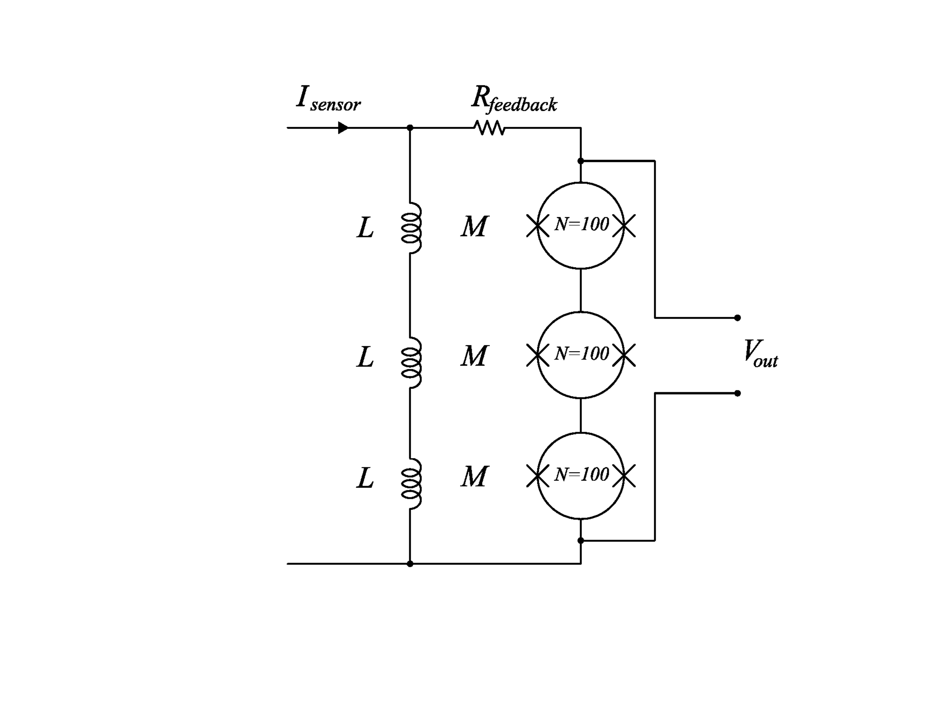
In designing and testing any SQUID FLL, we focus on four figures of merit: the closed loop gain , the forward gain, or transimpedance, , the input noise current , and the closed loop bandwidth of the system. The closed loop gain quantifies the ability of the feedback electronics to extend the dynamic range and linearity of the SQUIDs that form the LISA. The transimpedance measures the ratio of the LISA’s output voltage to the input current. The input noise current determines the sensitivity with which currents can be read out with the LISA. The closed loop bandwidth determines the number of sensors that can be multiplexed.
If the system consists of only an input-coil coupled SQUID-like component and a feedback resistor , the loop gain will be:
| (1) |
where and are the transimpedance and output impedance, respectively, of the series array SQUID combination shown in figure 2. The transimpedance is the product of the mutual inductance between the input coil and the SQUID inductance and the slope of the voltage response to applied flux:
| (2) |
A current supplied to the input coil of the LISA produces an output voltage . The LISA transimpedance is then
The expected current noise is a quadrature sum of the intrinsic noise from the component SQUID arrays, , and the Johnson noise of the feedback resistor, :
| (3) |
Equations 1 and III show a fundamental limitation on performance that depends on the properties of the individual SQUIDs that form the LISA. The output equivalent circuit is a voltage source with a series impedance inherent to the SQUIDs. The feedback current is then determined by the series combination of and while the output voltage of the LISA depends on the voltage divider formed by the output resistance and the parallel combination of the feedback resistance and the load presented by the capacitance of the cable connecting to the subsequent electronics at room temperature (assuming the warm amplifier’s input impedance is sufficiently to be negligible). Thus, for large output resistances the loop gain approaches the limit and the transimpedance approaches zero. In choosing or designing SQUIDs for the LISA, the ratio should be chosen to be as small as possible while maintaining the required overall transimpedance, . For a given load capacitance, also limits the achievable bandwidth.
IV Performance
As previously mentioned, our prototype LISA was designed with three SQUID array chips wired in series. The SQUID array on each chip has an input inductance of 160 nH, an input current noise of 2.5 pA/, a mutual inductance pH, a maximum transimpedance of , and an output impedance of . We chose a feedback resistance of .
IV.1 Tuning
Tuning a traditional SQUID device that includes room temperature feedback electronics typically involves first choosing a SQUID Josephson junction current bias that maximized the amplitude of the voltage-flux relation, then choosing an appropriate flux bias to maximize the SQUID transimpedance. Finally, a switch is closed, connecting the room temperature electronics output through a feedback resistor to the input coil of the SQUID device, enabling the flux-locked loop. The operating point of a flux-locked loop will jump by a single flux quantum if an input signal is applied that exceeds its dynamic range. Traditional flux-locked loops are restored to their original operating point by resetting the feedback either by interrupting the feedback signal momentarily and then re-locking or by turning the SQUID bias current to zero and then restoring it.
Because of its design, the cryogenic connection between the LISA output and input is inconvenient to open and close during the tuning process. However, tuning is very straightforward for the LISA. First we varied the SQUID Josephson junction current bias and for each bias current setting we measured the DC voltage-flux relation of the LISA. We chose the current bias that maximizes the dynamic range of the LISA (this ensures that we are biasing the constituent SQUIDs at a point close to the maximum of their individual voltage-flux responses). Then we used the measured optimum voltage-flux relation to determine the flux bias signal that moves the LISA to the middle of its dynamic range and applied this flux to the device. If the operating point of the LISA jumped in response to a signal that exceeded its dynamic range, the LISA was reset by momentarily interrupting its current bias.
IV.2 Dynamic Range and Linearity
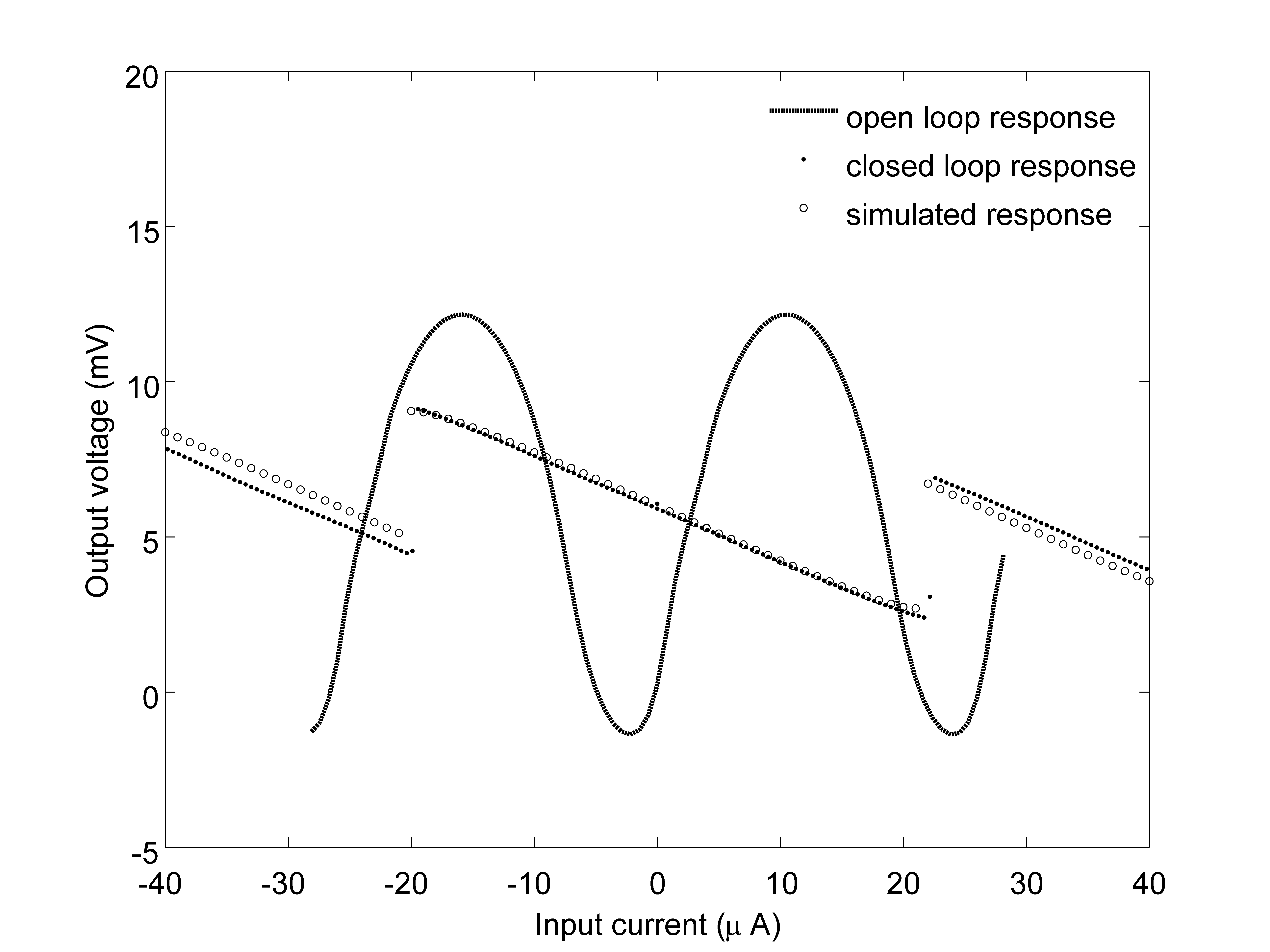
Once the LISA is tuned, we measure its dynamic range (maximum peak-to-peak applied signal) by applying a series of DC currents to the input coil and measuring the output voltages (voltage-current or voltage-flux relation). Figure 3 shows this measured relation for three SQUID devices in series without feedback, and the same relation for the LISA. The simulated response is also plotted in figure 3 Lanting (2006). The intrinsic sinusoidal response has been linearized over a dynamic range of and agrees well with the simulated response. Note that this measurement of dynamic range with a direct input current does not exactly apply to the high frequency response because of the 160 nH inductance of the input coil of each SQUID array. At 10 MHz, this corresponds to a reactance of from each SQUID array which slightly lowers the closed loop gain.
We expect that the dynamic range of the LISA, measured as a peak-to-peak current applied to the input coil, will be Spieler (2002)
| (4) |
where is the quantum of magnetic flux, is the mutual inductance between the input coil and each one of the constituent SQUIDs, and is the closed loop output impedance of the cold FLL as defined in section III. For the demonstration, we wired three 100-element series array SQUID chips in series. For an arbitrary number, , of series array SQUID chips, the loop gain becomes:
| (5) |
where and are the transimpedance and output resistance of the individual series array SQUID devices. As mentioned in section III, for a large number of devices in series, the loop gain approaches the limiting value of .
Using the properties of the individual LISA components used in this demonstration, we expect . This loop gain predicts, using equation 4, a dynamic range of 39 in good agreement with measurement.
The LISA has high linearity across most of its dynamic range, but exhibits gain suppression for large signals. We measure compression of dB at A with much smaller deviations from linearity for smaller signals.
IV.3 Bandwidth
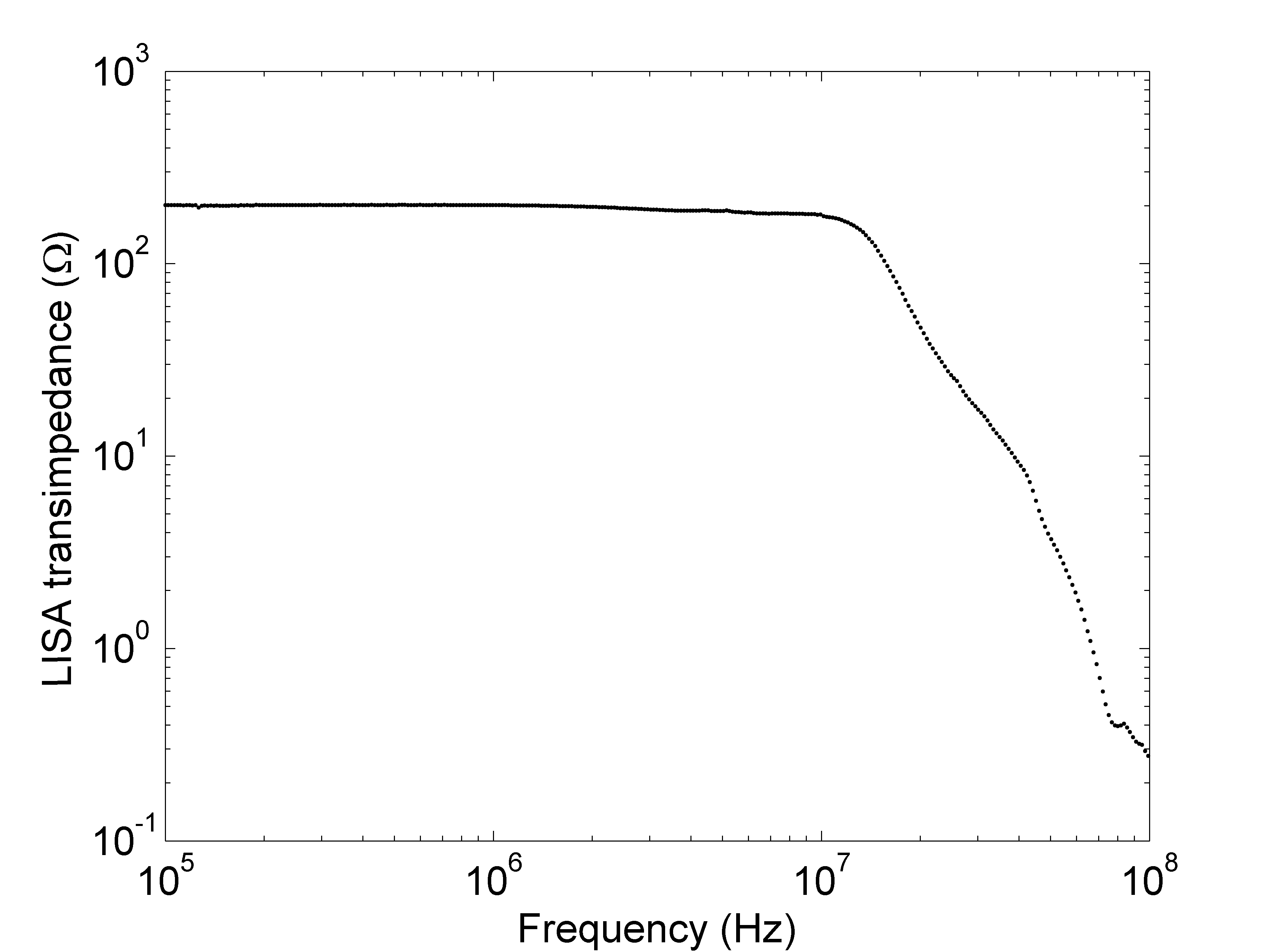
We measured the bandwidth of the LISA with a network analyser Hewlett-Packard . We applied a current of ARMS at the LISA input and measured the output voltage across three decades of frequency (0.1 MHz to 100 MHz). The current was applied differentially to the input coil of the LISA and the output voltage was amplified with room temperature electronics and then measured with a network analyser. We measure a small-signal bandwidth of MHz (see figure 4). We measure the large-signal bandwidth by recording the size of input current signal needed to induce flux jumping in the LISA as a function of frequency. The large-signal bandwidth achieved with the prototype setup is MHz. For our setup, the measured bandwidth is currently limited by several room temperature components: a stray capacitance of 50 pF at the input of the room temperature amplifier and the room temperature amplifier itself. Using a well-matched room temperature amplifier with low input capacitance and a larger designed bandwidth will increase the available LISA bandwidth.
IV.4 Noise
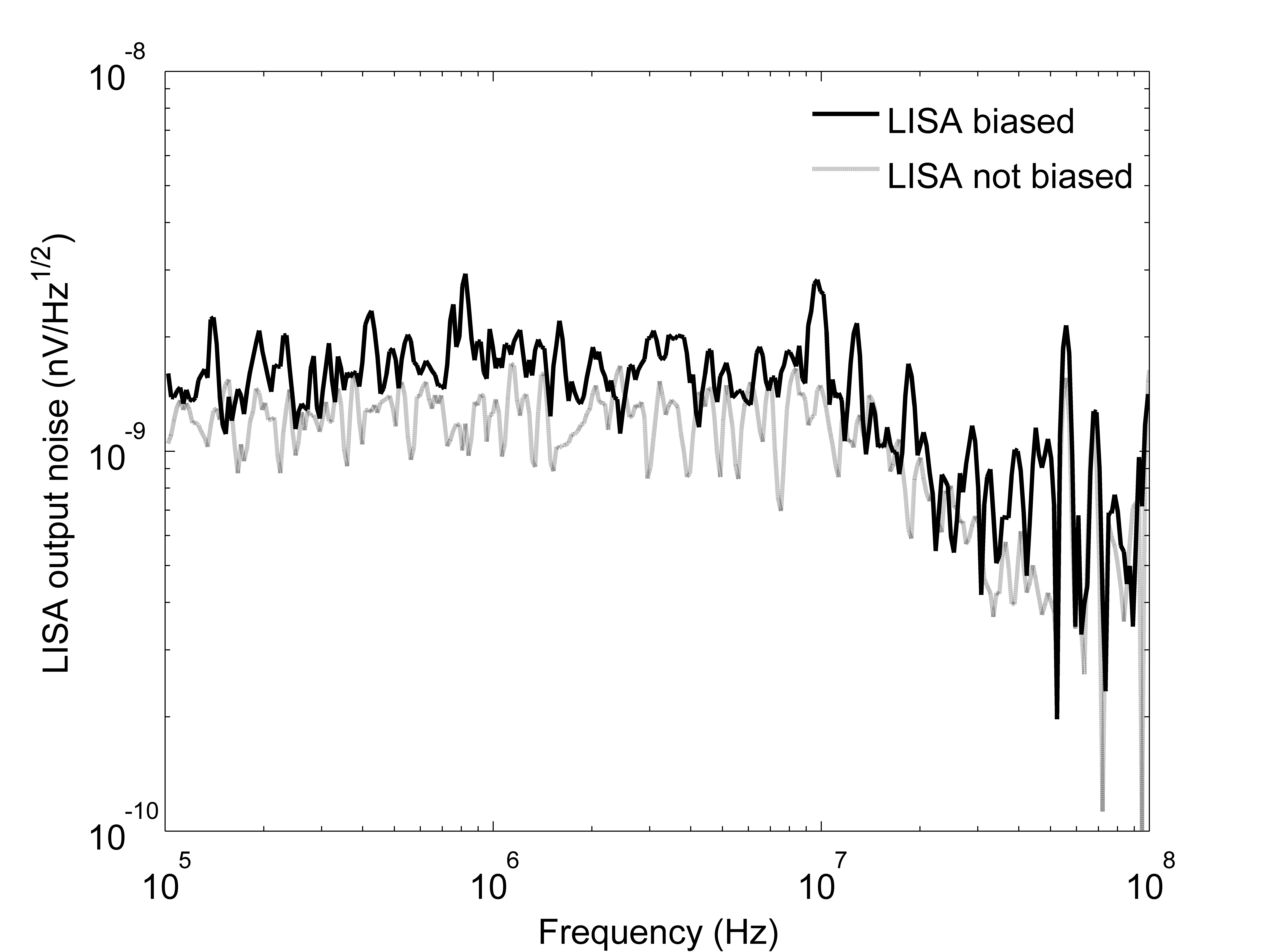
We coupled the output voltage of the LISA to a spectrum analyser and measured the noise from 1 to 100 MHz with the junction bias current on and off. The noise measured with the bias current off, 1.3 nV/, measures the baseline noise of the room temperature readout electronics. With the bias current on, the noise increases by 25 to 1.65 nV/. Figure 5 shows the measured noise spectra with the LISA bias current on and off. The expected combination of the Nyquist current noise from the feedback resistor and the intrinsic current noise from the individual SQUID devices predicts a total input voltage noise of 1.55 nV/, which is in agreement with the measured noise level. Referred to the input of the LISA, this measured noise is 8.25 pA/. This noise is currently dominated by the room temperature electronics and by increasing the transimpedance of the LISA, the referred current noise can be decreased.
V Conclusions
The performance of the prototype LISA is such that it meets the requirements for reading out multiplexed TES bolometers. The bandwidth is increased by an order of magnitude from current SQUID electronics, allowing the multiplexed channel count to increase by this same factor and the noise and dynamic range meet the design requirements. Finally, although the prototype consisted of three separate SQUID array chips, the underlying circuit is very simple. Future versions of this device can easily be integrated and manufactured on a single chip. The constituent SQUIDs should be designed to minimize the ratio to maximize the closed loop gain of the LISA.
VI Acknowledgements
We thank J. Clarke, D. Doering, and P. Richards for useful discussions. We also thank LBNL engineers John Joseph and Chinh Vu for their work on the room temperature electronics. Work at LBNL is supported by the Director, Office of Science, Office of High Energy and Nuclear Physics, of the U.S. Department of Energy under Contract No. DE-AC02-05CH11231.
References
- Audley et al. (2007) M. D. Audley, W. Holland, D. Atkinson, M. Cliffe, M. Ellis, X. Gao, D. Gostick, T. Hodson, D. Kelly, M. Macintosh, et al., SCUBA-2: A Large-Format CCD-Style Imager for Submillimeter Astronomy (Exploring the Cosmic Frontier: Astrophysical Instruments for the 21st Century, 2007), pp. 45–+.
- D. Schwan for the APEX-SZ Collaboration (2003) D. Schwan for the APEX-SZ Collaboration, New Astronomy Review 47, 933 (2003).
- Grainger et al. (2008) W. Grainger, A. M. Aboobaker, P. Ade, F. Aubin, C. Baccigalupi, É. Bissonnette, J. Borrill, M. Dobbs, S. Hanany, C. Hogen-Chin, et al., in Society of Photo-Optical Instrumentation Engineers (SPIE) Conference Series (2008), vol. 7020 of Presented at the Society of Photo-Optical Instrumentation Engineers (SPIE) Conference.
- Tran (2007) H. T. Tran, in Bulletin of the American Astronomical Society (2007), vol. 38 of Bulletin of the American Astronomical Society, pp. 271–+.
- Ruhl et al. (2004) J. Ruhl, P. A. R. Ade, J. E. Carlstrom, H.-M. Cho, T. Crawford, M. Dobbs, C. H. Greer, N. w. Halverson, W. L. Holzapfel, T. M. Lanting, et al., in Society of Photo-Optical Instrumentation Engineers (SPIE) Conference Series, edited by C. M. Bradford, P. A. R. Ade, J. E. Aguirre, J. J. Bock, M. Dragovan, L. Duband, L. Earle, J. Glenn, H. Matsuhara, B. J. Naylor, et al. (2004), vol. 5498 of Society of Photo-Optical Instrumentation Engineers (SPIE) Conference Series, pp. 11–29.
- Dobbs et al. (2007) M. Dobbs, E. Bissonnette, and H. Spieler, ArXiv e-prints 708 (2007), eprint 0708.2762.
- Lanting et al. (2004) T. M. Lanting, H. Cho, J. Clarke, M. Dobbs, A. T. Lee, M. Lueker, P. L. Richards, A. D. Smith, and H. G. Spieler, Nuclear Instruments and Methods in Physics Research A 520, 548 (2004).
- Spieler (2002) H. Spieler, in Monterey Far-IR, Sub-mm and mm Detector Technology Workshop proceedings, edited by J. Wolf, J. Farhoomand, and C. McCreight (2002), pp. 243–249, nASA/CP-2003-21140 and LBNL-49993, http://www-library.lbl.gov/docs/LBNL/499/93/PDF/LBNL-49993.pdf, URL http://www-library.lbl.gov/docs/LBNL/499/93/PDF/LBNL-49993.pd%f.
- Yoon et al. (2001) J. Yoon, J. Clarke, J. M. Gildemeister, A. T. Lee, M. J. Myers, P. L. Richards, and J. T. Skidmore, Applied Physics Letters 78, 371 (2001), URL http://adsabs.harvard.edu/cgi-bin/nph-bib_query?bibcode=2001A%pPhL..78..371Y&db_key=PHY.
- Oxley et al. (2004) P. Oxley, P. A. Ade, C. Baccigalupi, P. deBernardis, H.-M. Cho, M. J. Devlin, S. Hanany, B. R. Johnson, T. Jones, A. T. Lee, et al., in Infrared Spaceborne Remote Sensing XII. Edited by Strojnik, Marija. Proceedings of the SPIE, Volume 5543, pp. 320-331 (2004)., edited by M. Strojnik (2004), vol. 5543 of Presented at the Society of Photo-Optical Instrumentation Engineers (SPIE) Conference, pp. 320–331.
- Chervenak et al. (2000) J. A. Chervenak, E. N. Grossman, K. D. Irwin, J. M. Martinis, C. D. Reintsema, C. A. Allen, D. I. Bergman, S. H. Moseley, and R. Shafer, Nuclear Instruments and Methods in Physics Research A 444, 107 (2000).
- Chervenak et al. (1999) J. A. Chervenak, K. D. Irwin, E. N. Grossman, J. M. Martinis, C. D. Reintsema, and M. E. Huber, Applied Physics Letters 74, 4043 (1999), URL http://adsabs.harvard.edu/cgi-bin/nph-bib_query?bibcode=1999A%pPhL..74.4043C&db_key=PHY.
- M. Halpern (2007) M. Halpern, Proceedings of LTD 12 03 (2007).
- Irwin and Huber (2001) K. D. Irwin and M. E. Huber, IEEE Transactions on Applied Superconductivity 11(1), 1265 (2001).
- Huber et al. (2001) M. E. Huber, P. A. Neil, R. G. Benson, D. A. Burns, A. F. Corey, C. S. Flynn, Y. Kitaygorodskaya, O. Massihzadeh, J. M. Martinis, and G. C. Hilton, IEEE Transactions on Applied Superconductivity 11(2), 4048 (2001).
- Lanting (2006) T. M. Lanting (2006).
- (17) Hewlett-Packard, Hp4195a network/impedance analyzer.