InN dielectric function from the midinfrared to the visible range
L.A. Falkovsky
L.D. Landau Institute for Theoretical Physics, Moscow
117334, Russia
Institute of the High Pressure
Physics, Troitsk 142190, Russia
Abstract
The dispersion of the dielectric function for wurtzite InN
is analytically evaluated in the region near the fundamental energy gap.
The real part of the dielectric function has a logarithmic singularity at the
absorption edge. This results in the large contribution into the
optical dielectric constant. For samples with degenerate carriers,
the real part of the dielectric function is divergent at the
absorption edge. The divergence is smeared with temperatures or
relaxation rate. The imaginary part of the dielectric function
has a plateau far away from the absorption onset.
pacs:
71.15.Mb, 71.20.Nr, 78.20.Ci
Recently, InN has attracted considerable attention due to its
potential application as other III-nitrides, but especially owing
to the small energy band gap of about 0.7 eV
observed Da ; WWY ; NSY ; SSB ; BF in contrast to the value of 1.9
eV established for the last 20 years. The small band gap value
corresponds with a small effective electron mass WWS ; FC ; RWQ .
For future progress in the research field, reliable material
parameters are derived from the most widespread ab initio
electronic-structure calculations. However, these methods do not
present analytical results and lead sometimes to contradictions
BFJ , whether the 4d bands are included in the core or are
not. Therefore, the Hamiltonian is used to
clarify the physical content. In the corresponding Kane model
Ka for the wurtzite case, the conduction-band and the
valence-band are constructed from the and
, , and states at the
point.
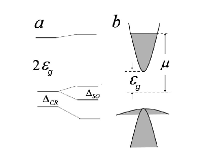
In Fig. 1a, the scheme of the valence-band splitting in InN
is shown under the crystal field
and the spin-orbit interaction .
According to experimental data GSW and calculations
RWQ , this splitting has a value on the order of eV, i. e. it is small in comparison with the band gap, and
can be ignored in calculations of the integral properties as the
optical absorption. Therefore,
the Kane model can be substantially simplified while using in
calculations of the dielectric function (DF).
Figure 1: (a) scheme of the valence-band splitting under the
crystal field and the SO interactions; (b) the electron band, the
heavy-hole and light-hole bands near the
point.
In this paper with the help of the simplified Kane model, we
evaluate analytically the DF for wurtzite InN in the range
eV, where the absorption is dominated by
optical transitions from three highest valence bands into the
lowest conduction band. As well known, the imaginary part of the
DF has the square-root behavior near the absorption edge in the
case, if the conduction-band is empty (i), and the step-like
behavior in the case, if the carriers in the conduction band are
degenerate (ii). In the paper FHF , the ab initio
calculations of the imaginary part were presented for the InN
polymorphs (with wurtzite, zinc-blend, and rocksalt structures) in
the case (i), whereas the real part was restored using the
Kramers-Kronig relations. In the paper FHF , the imaginary
part was also estimated within the Kane model, but these results
are misleading, because the optical-transition matrix elements are
incorrectly evaluated.
We find, that the real part of the DF has
at the absorption edge the kink-like singularity in the case (i)
and the logarithmic divergence in the case (ii). Such singularities have been
previously obtained for graphene FV and for IV-VI
semiconductors Fa . The singularities are smeared with
temperatures or carrier relaxation. The excitonic effects was not
observed in InN, since they are suppressed by the carrier
relaxation (see WWS ; FHF ; TDH for their estimation).
The effective Hamiltonian of the simplified anisotropic Kane model
is given as the matrix 44:
(1)
where are the interband
momentum-matrix elements with the velocity dimension (we put
in the intermediate formulas).
Quadratic terms in the
momentum can be written CC in the main diagonal
of the matrix (1), as well as in the terms, connecting the
states at the valence band top, . We omit them,
because their contribution in the DF is on the order of
, where
is the energy of the atomic scale.
This Hamiltonian (1) gives rise to the eigenvalues
(2)
corresponding with the conduction band and the light-hole band,
and the twofold eigenvalue
The effective masses at the conduction-band bottom are
(4)
for the longitudinal
and transverse directions respectively to the main axis.
Comparison with the values
and
eV obtained RWQ in the
experimental data analysis gives cm/sec,
cm/sec.
The velocity operator has the form
with orthonormal vectors chosen along the coordinate
axes.
Let us define the velocity matrix in the representation
diagonalizing the Hamiltonian (1):
Using the eigenfunctions of the Hamiltonian, one finds the matrix
:
where we use the notations ,
,
,
and is given in Eq. (2).
We note that the diagonal velocity-matrix elements in this
representation coincide with the derivative of the eigenvalues
and we write the off-diagonal elements
(5)
These matrix elements enter the general quantum-mechanic formula
for the dynamic conductivity
derived in the paper FV . Then, we obtain the DF with the
help of the relation
(6)
Due to the symmetry, the off-diagonal tensor components of the DF
vanish and there are only two independent components
and
.
The DF is separated into the intraband and interband parts. The
intraband term contains only the diagonal velocity-matrix elements
and has the Drude-Boltzmann form. For instance, we obtain for the
degenerate electrons:
(7)
where the chemical potential , the relaxation rate and
the photon frequency are written in the common units.
Neglecting the carrier relaxation, we can write the interband
term for the extraordinary component of the DF in the form
(8)
where is the
Fermi function. For the pristine semiconductor at low temperature,
the conduction band is empty, but the chemical potential can
be higher than the conduction band bottom in the
case of doping (see Fig. 1b).
The different terms in the braces present the verious optical
transitions: first, between the light-hole band and the
conduction band, second, between the heavy-hole band and the
conduction band, and third, between the light- and heavy-hole
bands. The infinitesimal in the denominators of Eq.
(InN dielectric function from the midinfrared to the visible range) defines the bypass around the poles. These bypasses
give the imaginary part of the DF, whereas the principal values of
the integrals yield the real part.
Transforming the integration variables
(9)
we integrate over the angles and :
The integral presenting the real part of the DF diverges
logarithmically at the upper limit. Since the leading contribution
arises from the values , the
integral can be cut off at the atomic value of energy
, where our expansion becomes
incorrect.
The imaginary part is easily evaluated for zero temperatures.
For instance, we find for the case ,
when electrons fill the conduction band,
(10)
where the step function conveys the condition for the
interband electron absorption.
Let us emphasize, that the band edge for the optical transitions
into the conduction band from the light-hole band at is higher than the edge for the transition from the
heavy-hole band at With increasing
the free electron concentration, both edges demonstrate the blue
Burstein-Moss shift.
At zero
temperatures, the chemical potential , measured from the
midgap is determined by the free-electron concentration:
If the electrons are absent in the conduction band,
, the imaginary part of the
DF is given in Eq. (InN dielectric function from the midinfrared to the visible range) with substitution
Far away from the absorption
edges, where , the imaginary part
demonstrates the plateau-like character with
(11)
The plateau noticed
also in the paper FHF and for the A4B6
semiconductors in Fa is a consequence of the linearity of
the electron dispersion at the energy larger in comparison with
the energy gap.
The real part of the DF contains the following contributions. The
transitions between the heavy-hole bands and the conduction band
give
(12)
where
(13)
if and
if
The transitions between the light-hole band and the conduction
band contribute
(14)
for and
(15)
for
We find that the real part of the DF as a function of
takes at the maximal value for :
where is the absorption
edge equal to or for the
corresponding transitions. If temperature plays a more important
role, we should put instead of in Eq. (17).
So far the extraordinary component was presented.
The ordinary component differs only in the factor
, which equals 0.98 for the experimental values of the
effective masses (4).
Now the value of the cutoff parameter is only
needed to calculate the DF. To estimate this value, we can use the
energy arising in the Kane model while the quadratic terms are
taken into account. According to estimations FHF ; RWQ , this
energy ranges from 8 to 15 eV. We take the intermediate value
eV plotting
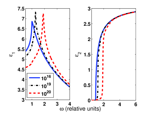
Figure 2: The real and imaginary parts of the DF versus the
photon frequency (in units of the gap eV)
for various free-electron concentrations, corresponding values of
the chemical potential are 1.01, 1.57, 2.79 (in units of
eV); relaxation rate 0,01
.
Fig. 2, where our theoretical results are shown. The maximum
value of the real part, Eq. (16), is found to equal 6.91
and the imaginary part of the DF takes the value 3.16 on the
plateau, Eq. (11). The corresponding values, , obtained from experiments
GSC ; KVM ; GWC and calculated from the first principles
FHF
are on the plateau in the frequency range eV.
That agrees very well with Fig. 2 (right panel).
The experiment KVM finds
the value about for the maximum of the real part.
The estimation KVM
of the dielectric constant gives .
The ab initio calculations
CG ; FHF find correspondingly in these two papers
and 7.16, as well as
and 7.27. The agreement with our Fig.
2 (left panel)
is excellent again. In our calculations, the maximum of the real part
for the large carrier concentration increases logarithmically with decreasing of
the relaxation rate. Plotting Fig. 2, we take
for various carrier concentrations.
Concerning the dielectric constant , we keep in
mind that the phonons contribute into its value. This
contribution can be estimated as
where is the transverse phonon frequency which is much
less
than the photon frequency considered here. Therefore, the phonon
contribution into
should be considered as negligible.
In conclusions, we find analytically that the real part of
the DF contains a singular contribution from the interband optical
transitions. It presents the large logarithmic term to the optical
dielectric constant. While increasing the frequency, we obtain the
dispersion of the dielectric function. Near the edge of the
interband absorption, a peak appears in the real part of the DF
for degenerate electrons filled the conduction band if the
relaxation rate is large enough.
This work was supported by the Russian Foundation for Basic
Research (grant No. 07-02-00571). The author is grateful to the
Max Planck Institute for the Physics of Complex Systems for
hospitality in Dresden.
References
(1) V. Y. Davydov et al., Phys. Status Solidi B
229, R1 (2002).
(2) J. Wu, W. Walukiewicz, K.M. Yu et al., Appl. Phys.
Lett. B 80, 3967 (2002).
(3) Y. Nanishi, Y. Saito, and T. Yamaguchi, Jpn. Appl.
Phys., Part 1 42, 2549 (2003).
(4) A. Sher, M. van Schilfgaarde, M.A. Berding et al.,
MRS Internet J. Nitride Semicond. Res. 4S1, G5.1 (1999).
(5) F. Bechstedt and J. Furthmüller, J. Cryst. Growth 246,
315 (2002).
(6) J. Wu, W. Walukiewicz, W. Shan et al., Phys. Rev.
B 66, 201403 (2002).
(8) Patric Rinke, M. Winkelnkemper, A. Qteish et al.,
Phys. Rev. B 77, 075202 (2008).
(9) D. Bagayoko, L. Franklin, H. Jin, and G.L. Zhao,
Phys. Rev. B 76, 037101 (2007).
(10) E.O. Kane, J. Phys. Chem. Solids 1, 249 (1957);
E.O. Kane, in Band Theory and Transport Properties, Handbook
on Semiconductors, vol. 1, ed. by W. Paul (North-Holand,
Amsterdam, 1982) p. 195.
(11) R. Goldhahn, P. Schley, A.T. Winzer et al.,
J. Cryst. Growth 288, 273 (2006).
(12) J. Furthmüller, P.H. Hahn, F. Fuchs, and F.
Bechstedt, Phys. Rev. B 72, 205106 (2005).
(13) L.A. Falkovsky, A.A. Varlamov, Eur. Phys. J. B
56, 281 (2006); L.A. Falkovsky, S.S. Pershoguba, Phys.
Rev. B 76, 153410 (2007).
(14) L.A. Falkovsky, Phys. Rev. B 77, 193201 (2008).
(15) J.S. Thakur, Y.V. Danylyuk, D. Haddat et al.,
Phys. Rev. B 76, 035309 (2007).
(16) S.L. Chuang and C.S. Chang, Phys. Rev. B 54, 2491 (1996).
(17) R.Goldhahn, S. Shokovets, V. Cimalla et al., Mater. Res. Soc. Symp.
Proc. 743, L5.9 (2003).
(18) A. Kasic, E. Valcheva, B. Monemar et al.,
Phys. Rev. B 70, 115217 (2004).
(19) R. Goldhahn, A.T. Winzer, V. Cimalla et al.,
Superlattices Microstruct. 36, 591 (2004).
(20) N.E. Christensen and I. Gorczyca, Phys. Rev. B 50,
4397 (1994).