Critical Current Behavior in Josephson Junctions with the Weak Ferromagnet PdNi
Abstract
We have studied the variation of critical current in Superconductor/Ferromagnet/Superconductor (S/F/S) Josephson Junctions as a function of ferromagnet thickness using a weakly-ferromagnetic alloy Pd82Ni12. Measurements were performed for the thickness range 32 to 100 nm, over which the critical current density decreases by five orders of magnitude. The critical current density oscillates with a period of nm, and decays over a characteristic length of nm. There is no evidence of a crossover to a slower decay, which might indicate the presence of long-range spin-triplet pair correlations. We discuss possible reasons for their absence, including the possibility of strong spin flip scattering in PdNi.
pacs:
74.50.+r, 74.45.+c, 75.30.Gw, 74.20.RpI Introduction
When a superconducting (S) metal is placed in contact with a normal (N) metal, the properties of both metals are modified near the S/N interface. The resulting superconducting proximity effect was widely studied in the 1960’s,deGennes and again in the 1990’s.LambertRaimondi ; Pannetier:2000 When the normal metal is replaced by a ferromagnetic (F) metal, the resulting physics is extremely rich, due to the very different order parameters in the two metals. There has been sustained interest in S/F systems over at least the past decade.BuzdinReview ; PokrovskyReview Many new phenomena have been observed, including but not limited to: oscillations in the critical temperature of S/F bilayers as a function of F layer thickness,Jiang:95 variations in the critical temperature of F/S/F trilayers as a function of the relative magnetization direction of the two F layers,Gu:02 and oscillations in the critical current of S/F/S Josephson junctions.Oboznov:06 The oscillatory behaviors are a direct result of the exchange splitting of the spin-up and spin-down bands in the ferromagnet, which produce a momentum shift between the up- and down-spin electrons of a Cooper pair that “leaks” from S into F.Demler In the clean limit, the spatial period of the oscillations is governed by the exchange length, , where and are the Fermi velocity and exchange energy of the F material, respectively.
Unlike the S/N proximity effect, which extends to distances of order 1 at sufficiently low temperature, the novel phenomena associated with the S/F proximity effect persist only over very short distances – limited either by , by the mean free path, , or by their geometric mean, the dirty-limit exchange length , where is the diffusion constant. These distance scales, characterizing the oscillation and decay of superconducting correlations, tend to be extremely short in strong ferromagnets, and only moderately longer in the weakly-ferromagnetic alloys preferred by some groups. For example, oscillations in the critical current in Nb/Co/Nb Josephson junctions have been observed with a period of 1.0 nm and a decay constant of 3.0 nm.Robinson:06 In Nb/Cu47Ni53/Nb alloy junctions, the observed period and decay constants were 11.0 nm and 1.3 nm, respectively.Oboznov:06
In this context, it was very exciting when two theoretical groups predicted that a new form of superconducting order, with spin-triplet pairing, could be induced by certain types of magnetic inhomogeneity in S/F systems consisting of conventional spin-singlet superconducting materials.Shekhter:01 ; Bergeret:01 ; Bergeret:03-1 ; Bergeret:03-2 Cooper pair correlations with spin-triplet symmetry are not subject to the exchange field of the ferromagnetic, since both electrons in the pair enter the same spin band in the ferromagnet. As a result, proximity effects due to such correlations should persist over long distances in a ferromagnetic, limited either by the temperature or by spin-flip and spin-orbit scattering. Furthermore, the spin-triplet correlations predicted to occur in S/F systems are not of same type discovered recently in materials such as SrRuO4.Eremin:04 In SrRuO4, the spin-triplet Cooper pairs satisfy the Spin-Statistics Theorem by having odd orbital angular momentum. In contrast, the spin-triplet correlations predicted to occur in S/F systems have even orbital angular momentum, and satisfy the Spin-Statistics Theorem by virtue of being odd in time or frequency.BergeretReview
Experimental confirmation of the presence of spin-triplet correlations is not easy. In retrospect, several theorists have suggested their role in old experiments performed on mesoscopic S/F hybrid samples, where the data were interpreted in terms of a long-range superconducting proximity effect.Giordano ; Petrashov ; Courtois More recently, there has been one report of a Josephson current in S/F/S structures using CrO2 as the F material,Keizer where the distance between the S layers was very long (several hundred nm), so that the conventional spin-singlet supercurrent should be exponentially suppressed. In a different work,Sosnin:06 phase-coherent oscillations were observed in the normal resistance of a Ho wire connected to two superconducting electrodes, again separated by a distance too large to support spin-singlet correlations. In both cases, the data were interpreted as being due to spin-triplet superconducting correlations in the ferromagnetic material. While these pioneering experiments are highly suggestive and tantalizing, the first suffers from large sample-to-sample fluctuations in the magnitude of the observed supercurrent,Keizer while both lack direct evidence for spin-triplet correlations.
The goal of this work is to study S/F/S Josephson junctions where the thickness of the F layer is increased systematically, from a thin regime where the supercurrent is likely to be dominated by spin-singlet correlations, to a thick regime where the smaller but longer-range spin-triplet supercurrent takes over. We chose Nb as the S material because its large critical temperature allows us to make measurements at 4.2 K, and hence measure a large number of samples. For the F material, we chose Pd1-xNix alloy with a Ni concentration of 12 atomic %, a material studied extensively by the group of M. ApriliKontos:01 ; Kontos:02 and others,Matsuda ; Cirillo ; Cirillo:02 ; Cirillo:03 ; Bauer but only with PdNi thicknesses less than 15 nm. Our choice of this particular weakly-ferromagnetic alloy was based on two considerations: 1) Using a weakly-ferromagnetic material allows us to increase the thickness of the F layer without introducing an overwhelming amount of intrinsic magnetic flux inside the junctions. (This issue will be discussed further in Section III below.) 2) Some weakly-ferromagnetic alloys suffer from strong spin-orbit and/or spin-flip scattering, which are likely to destroy both spin-singlet and spin-triplet correlations. For example, Ryazanov and co-workersRyazanov:01 ; Oboznov:06 have found that the Josephson current in S/F/S junctions using Cu1-xNix alloy with x = 53 at.% decreases exponentially over a length scale of only 1.3 nm. Moreover, that length scale is much shorter than the one characterizing the critical current oscillations, a fact that implicates strong spin-flip scattering in CuNi alloy.Demler ; Bergeret:03-2 ; Faure:06 In contrast, while Kontos et al.Kontos:02 found that the critical current in S/F/S junctions made with PdNi alloy decays over a length scale only slightly longer, 2.8 nm, they found that the oscillations and decay are governed by the same length scale, which may imply that spin-flip and spin-orbit scattering are weak in this material.
The paper is organized as follows. In Section II we discuss sample fabrication methods and characterization of the PdNi alloy. Section III discusses the characterization of our S/F/S Josephson junctions, with particular attention to the magnetic-field dependence of the critical current (the so-called “Fraunhofer pattern”). Section IV presents the main results of the paper, namely the critical current vs. PdNi thickness of our S/F/S Josephson junctions. Section V discusses the various theoretical works on S/F/S junctions, and the physical parameters that one can extract from fitting theoretical formulas to the data. Our interpretation of the results is presented in Section VI. Finally, we conclude with suggestions for future directions.
II Experimental
II.1 Sample Fabrication
Substrates were silicon chips of dimension mm. Preparation for deposition was performed in a cleanroom, to minimize the presence of dust particles which could lead to shorts in the Josephson junctions. A multilayer consisting of Nb(150)/PdNi(dPdNi)/Nb(25)/Au(15) (with all thicknesses in nm) was deposited using magnetically-enhanced triode dc sputtering in an Ar plasma pressure of 2.5 mTorr after obtaining a base pressure of 2 x Torr or better. A mechanical shadow mask was used to create the multilayer strip of size mm2. The thin Au protective layer prevents oxidation of the top Nb layer during further processing steps. The PdNi thickness, was varied from 32.5 nm to 100 nm, typically in 5 nm steps. A subset of samples was fabricated with more closely-spaced thicknesses in the range from 58 nm to 75 nm, in order to demonstrate the minima in critical current indicative of the transitions.
The multilayer was patterned using photolithography to create circular photoresist pillars with diameters of 10, 20, 40, and 80 on each substrate. Care was taken to ensure the presence of undercut in the resist profile. Either a trilayer photolithography consisting of two photoresist layers separated by a thin metallic layer or a single layer photolithography using chlorobenzene yielded large reliable undercuts in the resist profile. The large variation in area allowed us to have a large dynamic range for the critical current measurements. In practice, however, the success rate of the 80 pillars was very low, possibly due to the presence of dust particles during one of the fabrication steps taking place outside the cleanroom.
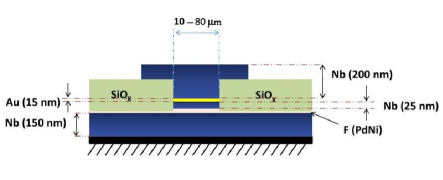
The photoresist pillars acted as a mask to protect the multilayer below them while the rest was ion milled. The multilayer was milled down to the middle of the ferromagnetic layer, thus completely removing the top Nb layer yet not exposing the bottom Nb layer, to prevent the possibility of back-sputtered Nb depositing on the sides of the circular pillars. Nearly 200 nm of was then deposited to insulate the bottom Nb from the top Nb leads. Lift off of the photoresist pillars was then done using Remover PG. This was followed by a slight ion milling of the top Au layer to ensure a clean interface. The top Nb lead of thickness 150 nm was then sputtered in the end. The thin Au layer becomes superconducting due to the proximity effect, as it is sandwiched between two Nb layers. A schematic of a complete Josephson junction is shown in Fig. 1.
II.2 Characterization of PdNi Alloy
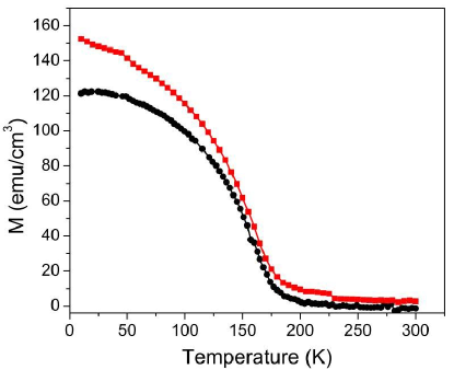
The Ni concentration of our PdNi alloy was estimated by three different methods. Energy dispersive X-ray analysis (EDAX), performed on a thick PdNi film, yielded a Ni concentration of . (A thick film was used for this measurement to increase the signal-to-noise ratio for the Ni-K peak. Similar measurements performed on 200-nm thick PdNi film yielded a similar concentration value provided the signal was accumulated for long enough times.) To corroborate this value for the concentration, the magnetization vs. temperature of a 100-nm thick PdNi film was measured using a Quantum Design SQUID magnetometer (see Fig. 2). A clear change in the slope is seen around the Curie temperature of about 175 K, independent of whether the magnetic field is applied in-plane or out-of-plane. This Curie temperature corresponds to a Ni concentration of , according to earlier work by Beille,Beille cited by Kontos.Kontos-thesis
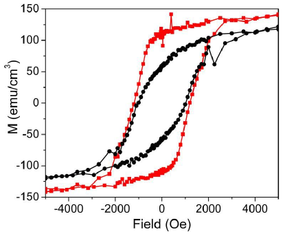
Fig. (3) shows vs. at K for the same 100-nm thick PdNi film. The magnetization curve is more rounded, and has smaller remanent magnetization, when the field is applied in-plane, indicating that the magnetic anisotropy of PdNi films is out-of-plane. Similar measurements on PdNi films of thickness 30 and 60 nm also indicate out-of-plane anisotropy, but somewhat less pronounced than in the 100-nm film. The out-of-plane anisotropy of PdNi surprised us initially, because the strong shape anisotropy of thin films usually dominates over magnetocrystalline anisotropy, resulting in overall in-plane anisotropy. Out-of-plane anisotropy has been observed in several materials, however, including CuNi alloy.Ruotolo ; Veshchunov Recently, we learned that Aprili has also observed out-of-plane anisotropy in PdNi films.Aprili_private The implications of PdNi’s out-of-plane anisotropy on our work will be discussed further at the end of this paper.
The saturation magnetization of PdNi measured out-of-plane at 10 K is emu/cm3 = 0.23 /atom (see Fig. 3). According to refs. [Beille, ; Kontos-thesis, ], this corresponds to a Ni concentration of nearly , in agreement with the determination from the EDAX measurements and Curie temperature.
II.3 Ic measurement
The normal-state resistances of our Josephson junction pillars vary from 2.4 to 152 , depending mostly on the pillar area, and, to a lesser extent, on the PdNi thickness. Resistances in this range require an extremely sensitive low noise measurement technique which is provided by using a superconducting quantum interference device (SQUID) as a null detector in a current-comparator circuit.EdmundsPratt All the four probe measurements were performed at 4.2 K by dipping the probe into a liquid Helium dewar equipped with a cryoperm shield. Each chip had Josephson junctions of diameters 10, 20, 40, and 80 . All measurements reported here were performed on junctions having Josephson penetration depth, larger than one-quarter of the junction diameter . ( is the superconducting flux quantum, is the critical current density, and is the London penetration depth, equal to about nm in our sputtered Nb.) This ensures uniform current density in the Josephson junction.Barone-Paterno If , then the flux is screened from the center of the junction (Meissner effect) and the effect of the self field cannot be neglected.
III Characterization of Josephson Junctions
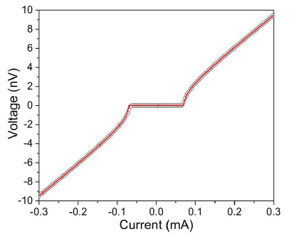
Fig. 4 shows a I-V relation typical for our S/F/S Josephson junctions. The curve follows the standard form for large-area, overdamped junctions:
| (1) |
Occasionally, we find that the I-V curves are shifted horizontally, so that the critical current is not exactly the same in the positive and negative current directions. In such cases, we average the critical currents in the two current directions.
One of the best ways to characterize Josephson junctions is to observe the modulation of critical current as a function of magnetic field applied perpendicular to the current flow direction in the junction. In nonmagnetic square junctions, the pattern so obtained is called the Fraunhofer pattern, due to its similarity to the pattern produced in single-slit diffraction of light. Observation of a good Fraunhofer pattern demonstrates that the supercurrent is uniform across the junction area, and that there are no short circuits in the surrounding SiOx insulator.
In nonmagnetic Josephson junctions with circular cross section and negligible screening (), the magnetic-field dependence of the critical current is given by
| (2) |
where is the critical current in the absence of magnetic field, is the Bessel function of the first kind of order 1, and is the magnetic flux penetrating the middle of the Josephson junction, with the London penetration depth, the diameter of the circular junction and the thickness of the barrier. This pattern is called an “Airy pattern.” The pattern is qualitatively similar to the Fraunhofer diffraction pattern, but the first minima are spaced more widely apart in field than the subsequent minima.
In samples containing a ferromagnetic barrier, one must include the intrinsic flux of the magnetic barrier on the Fraunhofer pattern. If the magnetization is uniform throughout the junction, the intrinsic magnetic flux is given by , with the F-layer thickness and the cross section width (equal to the diameter for circular junctions). In that case, the total magnetic flux through the F-layer is given by
| (3) |
In macroscopic samples the magnetization breaks into domains, and Eqn. (3) is not valid. Instead, one must integrate the current density across the area of the junction, taking into account the spatial dependence of the magnetic vector potential due to the domains. In the Coulomb gauge, one takes pointing along the current direction (z). The gauge-invariant phase difference across the junction includes a term proportional to the line integral of from deep inside one superconducting contact to deep inside the other.Levy The resulting expression for the supercurrent is:
| (4) |
where
| (5) |
The term containing the vector potential performs a random walk as one moves across the sample, due to the domains pointing in random directions. If the magnetic domains are very small and/or the magnetization is very weak, then the vector potential term stays near zero in all parts of the junction, and the critical current is hardly affected. If, however, the magnetic domains are large and/or have large magnetization as in the case of strong ferromagnet, the contribution to the phase due to the vector potential deviates far from zero as it crosses even a single domain, thus severely suppressing the critical current. This can lead to complete destruction of the Fraunhofer pattern. This is clearly seen in Fig. 5, which shows data for an S/F/S junction of diameter 10 , with an 11-nm thick Ni layer. (Similar random-looking “Fraunhofer patterns” have also been seen by other groups studying S/F/S Josephson junctions.Bourgeois:01 ) In principle, a regular Fraunhofer pattern can be recovered if the sample is completely magnetized, by applying a magnetic field in the opposite direction to the magnetization such that the total flux given by Eqn. (3) is zero. In that case, one should observe a regular Fraunhofer pattern shifted in field by an amount:
| (6) |
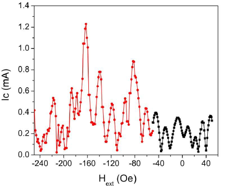
The above argument holds only if the coercive field of the magnetic material is large enough so that the magnetization stays nearly uniform even in the presence of the applied field, , pointing in the opposite direction. For the case of the Ni sample shown in Fig. 5, the largest peak in the critical current vs. field after magnetization is found near 160 Oe, whereas the expected shift calculated from the known saturation magnetization of Ni is about 207 Oe. The discrepancy is caused by some rotation of the magnetization in the domains or some domain wall motion as approaches the coercive field, which we measured to be approximately 180 Oe in a 9-nm Ni film.
To avoid the distortion of the Fraunhofer pattern, there are several options for the study of ferromagnetic Josephson junctions: 1) Use ultrathin samples: Under this condition the flux enclosed in the junction due to a single magnetic domain is much less than one flux quantum, and one can safely ignore the contribution to the flux from the magnetization. This option is not available to us, because our goal requires us to work with thick ferromagnetic layers. In addition, thin magnetic films often have magnetically ”dead” layers on each side, which pose additional problems for ultra thin samples; 2) Use samples with ultra-small lateral dimensions to reduce the contribution to the total magnetic flux from the magnetization, and to control the domain structure: This method has been pursued by Blamire and co-workers Robinson:07 and also by Strunk and co-workers,Strunk using strong ferromagnets. The disadvantage of this approach is that it becomes less effective as the thickness of the ferromagnetic layer is increased. In addition, it restricts the possibilities to introduce magnetic inhomogeneities that are naturally present due to the domain structure in devices of larger dimension, and which may be crucial for inducing the predicted spin-triplet superconducting correlations discussed in the Introduction; 3) Work with materials that either have weak magnetization, small domain size, or both: As discussed previously, this approach has been used by Ryazanov and co-workersRyazanov:01 ; Oboznov:06 who worked with CuNi alloy, and by Aprili and co-workers,Kontos:02 who worked with PdNi alloy. In CuNi alloy, Ryazanov demonstrated that the magnetization of the CuNi makes very little contribution to the total magnetic flux in his samples.Ryazanov:99 He did this by comparing the Fraunhofer pattern for a demagnetized sample with the pattern for the same sample uniformly magnetized. The latter pattern was shifted by a constant field, while the maximum value of the critical current was nearly unchanged. That shows that the integrated vector potential stayed close to zero everywhere in the sample; 4) Engineer the F layer to have zero net magnetic flux, for example, by using a “synthetic antiferromagnet.” We are currently exploring this option, and will report it in a future publication.Mazin
For this work, we have chosen the third option, but with PdNi alloy rather than CuNi alloy as our weak ferromagnet. As discussed in the introduction, there is evidence of strong spin-flip scattering in CuNi alloy, whereas the situation in PdNi alloy is less clear. It should be emphasized that the magnetism in PdNi is quite different from the magnetism in CuNi. Because Pd is nearly ferromagnetic itself according to the Stoner criterion, it takes only a small concentration of Ni to make the alloy ferromagnetic. One might expect then that the magnetism is more uniform in PdNi than in CuNi, where magnetism results from large Ni clusters.
As a final note regarding Nb/PdNi/Nb junctions, we found that using PdNi layers thinner than 30nm resulted in very large critical current densities – so large that even our smallest pillars (m) were in the regime . Kontos et al.Kontos:02 circumvented that problem by introducing an additional insulating layer in their junctions to reduce and hence increase . Because our interest is in studying junctions with large , we omitted the insulating layer. This choice limited our study to junctions with nm, which have small enough so that for our smallest diameter pillars.
IV S/F/S Josephson Junctions with PdNi: results
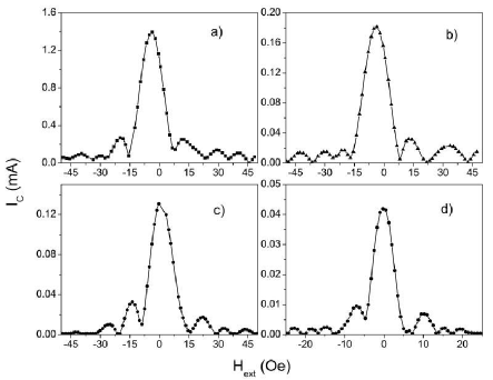
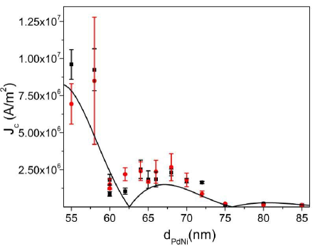
Fig. 6 shows vs. data for Nb/PdNi/Nb Josephson junctions with 35, 50, 70, and 85 nm of PdNi. The critical current has minima whenever an integer number of flux quanta penetrate the junction. The extremely low values of critical current at the minima indicate the absence of any shorts in the insulating material surrounding the Josephson junctions. Similar measurements were performed on samples for which the PdNi thickness varied from 35 nm to 100 nm. The maximum current density, , obtained for all such devices is plotted vs. thickness in Fig. 7. This figure represents the main result of this work. The error bars represent the standard deviation of the mean of the results obtained from several pillars on the same substrate. (For the smaller values of , we measured primarily the pillars of diameter 10 and 20 m, whereas for the larger values of , we measured the 20 and 40 m pillars.) The critical current density decreases exponentially over five orders of magnitude over this range of PdNi thickness. To our knowledge, these data represent the widest range of ferromagnet thickness in S/F/S Josephson junctions studied to date.
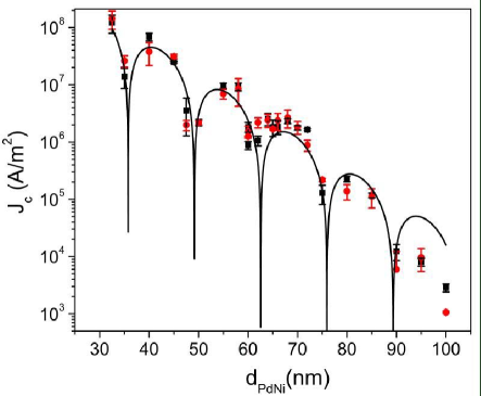
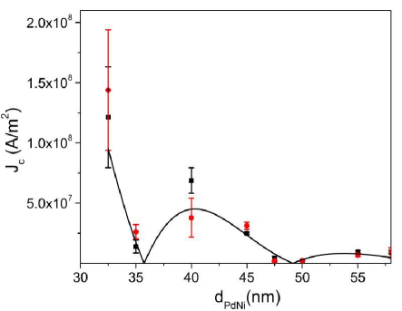
Fig. 7 shows that does not decrease monotonically with , but rather exhibits local minima with in the neighborhood of 35, 48, 60, and 75 nm. Figs. 8 and 9 show vs on linear axes, where the local minima are more clear. Such local minima have been observed in S/F/S junctions made with several different ferromagnetic materials,Oboznov:06 ; Kontos:02 ; Blum:02 ; Robinson:06 ; Sellier:03 ; Shelukhin:06 ; Weides:06 ; Weides:08 and signify transitions between standard junctions and -junctions.
Measurements of vs. were also performed on the samples after magnetizing them by applying an in-plane field of 5 kOe. The resulting Fraunhofer patterns (see Fig. 10) are shifted in field to a point where the flux due to the external field cancels out the flux due to the intrinsic magnetization. The maximum critical currents obtained for magnetized samples match closely with the virgin state data. This indicates that the domains in PdNi alloy are relatively small, so that the total excursion of the integrated vector potential as one crosses a domain is much less than one flux quantum.
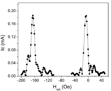
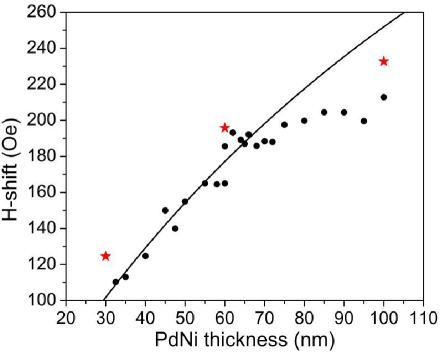
Fig. 11 shows the field shift of the Fraunhofer pattern of the magnetized samples, vs. PdNi thickness . As increases, the field shift saturates at a value near 200 Oe. As the PdNi thickness increases, there is an increasing tendency for the magnetization to rotate out of the plane, thereby decreasing its in-plane component. The solid line is a fit to the data of Eqn. 6, with the only free parameter being the remanent magnetization emu/cm3. This compares with values of 76 and 62 emu/cm3 measured directly on PdNi films of thickness 30 and 60 nm, respectively. The red stars in Fig. 11 show the values of calculated from Eq. 6, using the values of measured directly on PdNi films of thickness 30, 60, and 100 nm. The agreement with the field shifts of the Fraunhofer patterns is reasonable.
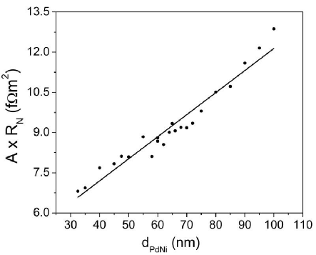
We have also measured the normal-state resistance of our samples at currents much larger than . A plot of the specific resistance (area times resistance) vs. is shown in Fig. 12. The interface and bulk contributions to are given by:
| (7) |
where is the resistivity of PdNi, is the thickness of the PdNi layer, and is the Nb/PdNi boundary resistance. A linear fit to all of the data gives a boundary resistance of and a resistivity of PdNi, . There is some indication in the data that the slope increases for greater than about 75 nm. If we fit only the data for nm, then we find and . Independent measurements of the in-plane PdNi resistivity were performed on 200-nm thick films, using the van der Pauw method. Those measurements produced the value . It is plausible that the in-plane resistivity is larger than the perpendicular resistivity if the PdNi films grow in a columnar fashion, although measurements on other sputtered metals often find quite close agreement between these two measurement methods.BassPratt
V Theory of S/F/S Josephson Junctions
There have been a large number of theoretical works dealing with S/F/S Josephson junctions. There are three energy scales whose relative size determines three distinct regimes. The energy scales are the exchange energy in the ferromagnet, , the gap in the superconductor, , and , the inverse of the mean free time between collisions of an electron propagating in the ferromagnet. In all of the experimental work on S/F/S Josephson junctions published to date, including this work, . There is a wide variation, however, in the size of relative to those two energies. The true clean limit is expressed by , which also implies . The intermediate limit is where but , whereas the true dirty limit is where both and . These three regimes can also be characterized by the relative sizes of the three length scales: the electron mean free path, , the superconducting coherence length, , and the clean-limit exchange length discussed earlier, .
The simplest limit is the dirty limit, with the additional constraint that the ferromagnetism is weak enough so that one can treat the spin-up and spin-down bands identically, i.e. as having the same Fermi velocity and mean free path. In this limit, the Usadel equation is valid. An expression for the critical current as a function of ferromagnetic layer thickness was first derived by Buzdin et al.Buzdin:92 In this regime, the oscillation and decay of as a function of are both governed by a single length scale – the ”dirty-limit” exchange length, . Once exceeds , the thickness dependence of takes the simple form:
| (8) |
In the presence of spin-flip or spin-orbit scattering, Eqn (8) is modified, and the length scales governing the decay and the oscillation are no longer equal.Faure:06 ; Bergeret:03-2 ; Demler ; Bergeret:07 The more general form can be written as
| (9) |
In general, the effect of spin-flip or spin-orbit scattering is to shorten the decay length scale, , relative to , and to lengthen the oscillation length scale, . In the presence of sufficiently strong spin-orbit (but not spin-flip) scattering, the oscillations disappear completely. An equation similar to Eqn. (9) has successfully been used to fit vs. data from S/F/S junctions containing CuNi alloy, with nm, and nm.Oboznov:06 The very short value of compared to was interpreted as implying that spin-flip scattering is strong in that material.
Eqn. (9) can also be fit to our data, as shown in Figs. 7-9. But in our case, the length scale governing the exponential decay (nm) is considerably longer than the length scale governing the oscillation (nm), hence the dirty-limit hypotheses that led to Eqn. (9) are not fulfilled. However, the condition has also observed in S/F/S Josephson junctions containing the strong ferromagnets: Ni, Fe, Co, and Ni80Fe20 (also known as Permalloy, or Py).Robinson:06 Those materials have very large exchange energy, hence they are in the intermediate limit, with but still . Our observation of in S/F/S junctions with PdNi alloy suggest that PdNi may also be in the intermediate limit.
The intermediate limit has been studied in several theoretical papers. Bergeret et al.Bergeret:01 provide a general formula for the critical current, valid both in the dirty limit and intermediate limit. In the intermediate limit the formula simplifies when the F-layer thickness is larger than the mean free path. Eqn. (20) from ref. Bergeret:01, is:
| (10) |
where the sum is over the positive Matsubara frequencies, with the temperature. Asymptotically at large values of , Eqn. (10) is quite similar to Eqn. (9), with and . Nevertheless, we have fit Eqn. (10) directly to our data, and obtained the parameters nm and nm. Not surprisingly, the former agrees closely with the value of obtained from the fit of Eqn. (9), while the value of obtained from Eqn. (10) is somewhat larger than the value of obtained from the fit of Eqn. (9) – the difference undoubtedly due to the sum over Matsubara frequencies in Eqn. (10). We will use the larger value of in the following discussion.
An alternative theoretical approach was taken by Kashuba, Blanter, and Fal’ko,Kashuba who considered a model of S/F/S junctions taking explicit account of spin-dependent and spin-flip scattering in the F layer. In the intermediate limit, these authors find a result that is nearly identical to Eqn. (10).
VI Discussion of Results
VI.1 Estimate of mean free path and exchange energy in PdNi
In many metals, it is straightforward to estimate the mean free path directly from the measured resistivity, as the product is inversely proportional to the Fermi surface area, and has been tabulated for a large number of metals.BassLandolt In PdNi alloy, however, the product is not known. Some workers have tried to estimate in PdNi from its value in Pd, but even that estimation is not straightforward, due to the complex band structure of Pd. To illustrate the difficulty, previous workers have quoted values of the product as small as (refs. Cirillo, ; Matsuda, ) and as large as (ref. Kontos-thesis, ). The former value is certainly too small, because it was calculated using the Einstein relation, , with the density of states at the Fermi level, , obtained from the electronic specific heat coefficient . The problem is that, in Pd, the specific heat is dominated by heavy holes on the open “jungle gym” portion of the Fermi surface, while the electronic transport is dominated by much lighter electrons on a part of the surface centered at the -point. (It is common to refer to these electrons as “s-like”; but that is incorrect because they are strongly hybridized with the d bands.Pinski ) Discussion of the Fermi surface in Pd has been given in several papers.Pinski ; Vuillemin ; Dye ; Mazin:1984 Pinski et al.Pinski state that the -centered sheet of the Fermi surface carries the vast majority of the transport current – up to 97% at 10 K.
We estimate the product for PdNi in two ways. In his Ph.D. thesis,Kontos-thesis Kontos found that the resistivity of thin PdNi films with varied linearly with inverse thickness once the films were thinner than about 8 nm, indicating that the mean free path is limited by the film thickness. The slope of the graph gives the product . We expect the product to be within a factor of two of this value. The second method relies on the statement by Pinksi et al.Pinski that electronic transport in Pd is dominated by the electrons on the -centered sheet. The total number of carriers in that band, the density of states at the Fermi level, the effective mass, and the Fermi velocity on that sheet have all been tabulated by Dye et al.Dye based on deHaas van-Alphen measurements of the Fermi surface of Pd. The values of those four quantities are: carriers/atom ; states/(eV atom spin) ; ; and m/s.DumoulinNote Using the Drude formula, , one finds , while using the Einstein relation one finds . (The slight difference between the two values is likely due to the non-parabolic character of the -centered sheet.) These values are close to the value estimated from the thickness dependence found by Kontos. If we take our own measured resistivity, , and the value of the mean free path from the vs. fit, nm, we obtain , which is not too far from the estimates given above. (The only mystery we can not explain from this analysis is the very low value of the Fermi velocity, m/s, measured by Dumoulin et al.Dumoulin in a proximity effect experiment between Pb and Pd. It is unclear why that experiment measures the low Fermi velocity of the open hole sheet rather than the higher Fermi velocity of the -centered sheet.)
| Source | Experiment | Ni conc. | formula to | ||||||||
| (at. %) | (m/s) | (fm2) | (nm) | (nm) | (nm) | (nm) | (meV) | extract | (K) | ||
| Kontos:01, | S/F DOS | 10 | 2.0 | 4 | - | 2.8 | 2.8 | 35 | 100 | ||
| Kontos:02, | S/I/F/S | 12 | 2.0 | 4 | - | 3.5 | 3.5 | 13 | 260 | ||
| Cirillo, | of S/F | 14 | 2.0 | 4 | 240 | 16.6 | 6 | 6 | 15 | 156 | |
| Cirillo:02,; Cirillo:03, | of S/F | 14 | 2.0 | 0.96 | 240 | 4 | 3.4 | 3.4 | 13 | 185 | |
| Matsuda, | of S/F | 15 | 2.0 | 0.3256 | 220 | 1.48 | 3.5 | 3.5 | 13 | 260 | |
| Bauer, | S/F/S | 18 | 2.0 | - | - | - | 2.4 | 2.4 | 52 | 200 | |
| this work | S/F/S | 12 | 5.6 | 1.0 | 82 | 11 | 8.0 | 4.0 | 44 | 175 |
From the period of oscillation of vs. , we found nm. Using the Fermi velocity of the dominant carriers, m/s, gives an estimate for the exchange energy in our Pd88Ni12 alloy of meV. This value is somewhat higher than values quoted by previous workers Kontos:02 ; Cirillo ; Cirillo:02 ; Cirillo:03 ; Matsuda , but those earlier estimates were either made using the smaller value of , or using the diffusive formula . A more meaningful comparison is of the length scales and found in different experiments. For example, Kontos et al.Kontos:02 found in their study of S/I/F/S Josephson junctions with a PdNi alloy of similar concentration to ours. The values of in their experiment and ours are rather close to each other, but the values of are not. It is not clear if that discrepancy is significant or not. The thickness range covered in the earlier work was 4.5 - 14 nm, whereas the range we covered was 32.5 - 100 nm. If the mean free path in the PdNi alloy is indeed in the range of 11 nm, then the samples studied by Kontos et al. were in the crossover regime with , where the thickness dependence has not yet obtained the asymptotic exponential decay, . But then one would expect a less steep decay of with , rather than a more steep decay. Perhaps a more relevant observation is simply that the PdNi films deposited in different laboratories may have different polycrystalline structures, and hence very different mean free paths. A summary of the parameters estimated by previous workers, as well as by our work, is given in Table I.
VI.2 Spin-triplet superconducting correlations?
One of the primary goals of this work was to search for signs of spin-triplet superconducting correlations in our samples. At first glance, the data in Fig. (7) show no sign of spin-triplet superconducting correlations, which might manifest themselves as a crossover to a less-steep exponential decay of at large values of . It is intriguing, however, that the length scale characterizing the exponential decay of in our samples, nm, is substantially longer than that observed previously in shorter S/F/S junctions with PdNi.Kontos:02 Could it be that we are already observing the triplet Josephson effect throughout the whole range of reported here? The strongest evidence against such an interpretation is the nearly-periodic set of local minima we observe in vs. , shown in Figures (7-9). We believe that those local minima signal crossovers between 0-junctions and -junctions, which are due to the effect of the exchange splitting on spin-singlet superconducting correlations. A Josephson supercurrent dominated by spin-triplet correlations would not exhibit such minima, but rather would decay monotonically with increasing . Nevertheless, to rule out the spin-triplet hypothesis definitively would require stronger evidence that the local minima we observe truly represent crossovers, rather than an unlucky distribution of uncertainties in the data that mimics a periodic set of local minima.
There are three ways one could make a more stringent test that the local minima observed in our vs. data are due to crossovers: 1) A direct measurement of the current-phase relationship of the junction;Frolov:2004 2) Extension of vs. measurements to smaller values of , to see if the slope of the vs. semi-log plot changes to a value close to that measured by Kontos et al.. This would require reducing the lateral size of our junctions, so as to maintain the condition ; 3) Measurement of vs. temperature for samples very close to a crossover. In S/F/S junctions with very weak ferromagnets, the crossover has been observed in the -dependence of .Oboznov:06 ; Ryazanov:01 ; Sellier:03 ; Weides:08 As the exchange energy increases, however, the thickness range over which one can see a non-monotonic -dependence of gets progressively narrower.Weides:08 Each of these checks presents its own set of challenges, and represents a possible direction for future work.
VI.3 Spin-flip scattering in PdNi
Assuming that our data are not the result of spin-triplet correlations, we would like to know why not. There are several factors that may contribute. First and foremost, strong spin-flip scattering, if it exists in our PdNi alloy, would destroy the triplet correlations. To address this issue, we have independently tried to measure directly the spin diffusion length, , in PdNi alloy using techniques borrowed from the Giant Magnetoresistance (GMR) community. A complete discussion of those measurements is given elsewhere.Hamood Here we note the most salient results. First, the value of the spin diffusion length obtained, , is extremely surprising given the much longer length scale characterizing the decay of the Josephson supercurrent in the present work. Normally, one assumes that spin-flip and spin-orbit scattering processes occur on length scales much longer than the mean free path, justifying the diffusive model used in discussing the spin diffusion length.ValetFert:93 Hence a measurement of a spin diffusion length several times shorter than the mean free path is difficult to interpret. We believe that the very short value of observed using a GMR spin valveHamood may be due to the out-of-plane magnetic anisotropy of PdNi discussed earlier. The analysis of the spin-valve data of ref. Hamood, assume that the magnetizations of the two magnetic layers are either parallel or antiparallel to each other. Our recent discovery of the out-of-plane magnetic anisotropy in PdNi casts doubt on this assumption. It is possible that the magnetization of PdNi is inhomogeneous on very short length scales, which may then destroy spin memory by rotating the spin on a length scale smaller than the mean free path. Clarifying this issue will require further experiments.
A second possible reason we do not observe signs of spin-triplet superconducting correlations is that the length scale characterizing the magnetic inhomogeneity in PdNi might not be comparable to the Cooper pair coherence length in Nb. Let us refer to the length scale characterizing the magnetic inhomogeneity as . If , then a Cooper pair will experience the magnetization averaged over the length , and triplet correlations will not be produced efficiently. If , then a typical Cooper pair experiences no magnetic inhomogeneity. The coherence length in our Nb is known to be about 13 nm.Gu:02 Unfortunately, the typical domain sizes and domain wall widths in our PdNi alloy are not known. Because the Curie temperature of PdNi is well below room temperature, obtaining information about magnetic structure requires a low temperature magnetic visualization technique, such as low-temperature magnetic force microscopy (MFM) or Bitter decoration. And even then, the former method is not well-suited to weak ferromagnets, because the magnetization of the MFM tip may influence the domain structure of the sample. Very recently the domain structure of CuNi alloy was measured using the Bitter decoration technique.Veshchunov Those measurements confirmed the out-of-plane magnetic anisotropy of that material, and found a typical domain size of 100nm in the virgin state or at the coercive field. Unfortunately, no such measurements have been performed on PdNi alloy, to our knowledge. Clearly, a thorough study of the magnetic domain structure of PdNi would help clarify this issue.
VII Future Directions
The most urgent work needed in the future is a strong verification (or repudiation) that the local minima in our data do indeed represent crossovers, rather than sample-to-sample fluctuations. Looking further ahead, to have any hope of nailing down the elusive spin-triplet supercurrent in S/F/S junctions will require better characterization of magnetic materials. On the one hand, the spin diffusion length is a crucial parameter, as it limits the spatial extent of spin-triplet correlations. Fortunately, the spin-diffusion length has been measured in some ferromagnetic materials,BassPrattReview but more work is needed. Of equal important is information about the typical length scales characterizing the domain structure of ferromagnetic thin films. This is a complex issue, as either the domain size or domain wall width may be important. For example, in a film where neighboring domains have antiparallel magnetization, the long-range triplet component is generated only in the domain walls,Fominov:07 hence it is crucial that the domain wall width be comparable to . If, however, neighboring domains have non-collinear magnetizations, then it would seem that the long-range triplet could be produced even if the domain walls are very thin, as long as the typical domain size is comparable to . Unfortunately, domain sizes in polycrystalline films are not known a priori.OHandleyBook
VIII Conclusions
We have measured the critical current of Nb/PdNi/Nb Josephson junctions with PdNi thicknesses ranging from 32.5 to 100 nm. The critical current drops by five orders of magnitude over this thickness range. The data appear to have a periodic array of local minima, suggesting that the supercurrent is of the conventional spin-singlet type over the entire thickness range. We have discussed possible reasons for the absence of induced spin-triplet correlations, such as spin-flip scattering or a poor match of length scales between the magnetic domains and the superconducting coherence length.
IX Acknowledgements
We are grateful to M. Aprili, Y. Blanter, T. Kontos, and V. Ryazanov for helpful discussions, and to B. Bi, R. Loloee, and Y. Wang for technical assistance. This work was supported by the Department of Energy under grant ER-46341.
References
- (1) P.G. de Gennes, Rev. Mod. Phys. 36, 225 (1964).
- (2) C.J. Lambert and R. Raimondi, J. Phys. Condens. Matter 10, 901 (1998).
- (3) B. Pannetier and H. Courtois, J. Low Temp. Phys. 118, 599 (2000).
- (4) A.I. Buzdin, Rev. Mod. Phys. 77, 935 (2005).
- (5) I.F. Lyuksyutov and V.L. Pokrovsky, Ad. Phys. 54, 67 (2005).
- (6) J.S. Jiang, D. Davidovic, D.H. Reich, and C.L. Chien, Phys. Rev. Lett. 74, 314 (1995).
- (7) J.Y. Gu, C.-Y. You, J.S. Jiang, J. Pearson, Ya.B. Bazaliy, and S.D. Bader, Phys. Rev. Lett. 89, 267001 (2002).
- (8) V.A. Oboznov, V.V. Bol’ginov, A.K. Feofanov, V.V. Ryazanov, and A.I. Buzdin, Phys. Rev. Lett. 96, 197003 (2006).
- (9) E.A. Demler, G.B. Arnold, and M.R. Beasley, Phys. Rev. B 55, 15174 (1997).
- (10) J.W.A. Robinson, S. Piano, G. Burnell, C. Bell and M.G. Blamire, Phys. Rev. Lett. 97, 177003 (2006).
- (11) A. Kadigrobov, R.I. Shekhter, and M. Jonson, Europhys. Lett. 54(3), 394 (2001).
- (12) F.S. Bergeret, A.F. Volkov, and K.B. Efetov, Phys. Rev. B 64, 134506 (2001).
- (13) A.F. Volkov, F.S. Bergeret, and K.B. Efetov, Phys. Rev. Lett. 90, 117006 (2003).
- (14) F.S. Bergeret, A.F. Volkov, and K.B. Efetov, Phys. Rev. B 68(6) 064513 (2003).
- (15) Eremin, I., D. Manske, S. G. Ovchinnikov, and J. F. Annett, Ann. Phys. 13, 149 (2004).
- (16) F.S. Bergeret, A.F. Volkov, K.B. Efetov, Rev. Mod. Phys. 77, 1321 (2005).
- (17) M.D. Lawrence, and N. Giordano, J. Phys.: Condens. Matter 8, 563 (1996) and J. Phys.: Condens. Matter 11, 1089 (1999).
- (18) V.T. Petrashov, I.A. Sosnin, I. Cox, A. Parsons, and C. Troadec, Phys. Rev. Lett. 83, 3281 (1999).
- (19) M. Giroud, H. Courtois, K. Hasselbach, D. Mailly, and B. Pannetier, Phys. Rev. B 58, R11872 (1998).
- (20) R.S. Keizer, S.T.B. Goennenwein, T.M. Klapwijk, G. Xiao, and A. Gupta, Nature (London) 439, 825 (2006).
- (21) I. Sosnin, H. Cho, V.T. Petrashov, and A.F. Volkov, Phys. Rev. Lett. 96, 157002 (2006).
- (22) T. Kontos, M. Aprili, J. Lesueur, and X. Grison, Phys. Rev. Lett. 86, 304 (2001).
- (23) T. Kontos, M. Aprili, J. Lesueur, F. Genet, B. Stephanidis, and R. Boursier, Phys. Rev. Lett. 89, 137007 (2002).
- (24) K. Matsuda, H. Niwa, Y. Akimoto, T. Uemura, and M. Yamamoto, IEEE Trans. Applied Superconductivity. vol. 17, No. 2, JUNE 2007.
- (25) C. Cirillo, S.L. Prischepa, M. Salvato, C. Attanasio, Journal of Physics and Chemistry of Solids 67, 412 (2006).
- (26) C. Cirillo, J. Aarts, and C. Attanasio, Phys. Stat. Sol. (c) 3, No. 9, 3015 (2006).
- (27) C. Cirillo, S. L. Prischepa, M. Salvato, C. Attanasio, M. Hesselberth and J. Aarts, Phys. Rev. B 72, 144511 (2005).
- (28) A. Bauer, J. Bentner, M. Aprili, M. L. Della Rocca, M. Reinwald, W. Wegscheider, and C. Strunk, Phys. Rev. Lett. 92, 217001 (2004).
- (29) V.V. Ryazanov, V.A. Oboznov, A.Yu. Rusanov, A.V. Veretennikov, A.A. Golubov, and J. Aarts, Phys. Rev. Lett. 86, 2427 (2001).
- (30) M. Faure, A.I. Buzdin, A.A. Golubov, and M.Yu. Kupriyanov: Phys. Rev. B 73, 064505 (2006).
- (31) José Beille, Ph.D. thesis, Université Joseph Fourier, Grenoble (1975).
- (32) T. Kontos, Ph.D. thesis, Université Paris XI, Orsay (2002).
- (33) A. Ruotolo, C. Bell, C.W. Leung, and M.G. Blamire, Journal of Applied Physics, Vol. 96., No. 1 (2004).
- (34) I.S. Veshchunov, V.A. Oboznov, A.N. Rossolenko, A.S. Prokofiev, L.Ya. Vinnikov, A¿Yu. Rusanov, and D.V. Matveev, arXiv:0811.2331 (2008).
- (35) M. Aprili, private communication.
- (36) D. Edmunds, W. Pratt, and J. Rowlands, Rev. of Sci. Instr. 51, 1516 (1980).
- (37) A. Barone and G. Paterno, Physics and Applications of the Josephson Effect, John Wiley & Sons (1982).
- (38) L. P. Lévy, Magnetism and Superconductivity, Springer-Verlag, Berlin (2000).
- (39) O. Bouregois, P. Gandit, J. Lesueur, A. Sulpice, X. Grison, and J. Chaussy, Eur. Phys. J. B 21, 75 (2001).
- (40) J.W.A. Robinson, S. Piano, G. Burnell, C. Bell and M. G. Blamire, Phys. Rev. B 76, 094522 (2007).
- (41) C. Srgers, T. Hoss, C. Schnenberger, C. Strunk, J. Magn. Magn. Mat., 240, 598 (2002).
- (42) V.V. Ryazanov, Physics-Uspekhi 42, 825 (1999).
- (43) M. Khasawneh, W.P. Pratt, Jr, and N.O. Birge, unpublished.
- (44) Y. Blum, A. Tsukernik, M. Karpovski, and A. Palevski, Phys. Rev. Lett. 89, 187004 (2002).
- (45) H. Sellier, C. Baraduc, F. Lefloch, and R. Calemczuk, Phys. Rev. B 68, 054531 (2003).
- (46) V. Shelukhin, A. Tsukernik, M. Karpovski, Y. Blum, K.B. Efetov, A.F. Volkov, T. Champel, M. Eschrig, T. Lfwander, G. Schn, and A. Palevski, Phys. Rev. B 73, 174506 (2006).
- (47) M. Weides, M. Kemmler, E. Goldobin, D. Koelle, R. Kleiner, H. Kohlshedt, and A. Buzdin, Appl. Phys. Lett. 89, 122511 (2006).
- (48) A.A. Bannykh, J. Pfeiffer, V.S. Stolyarov, I.E. Batov, V.V. Ryazanov, M. Weides, arXiv:0808.3332v2 [cond-mat.supr-con] (2008).
- (49) S. -F. Lee, Q. Yang, P. Holody, R. Loloee, J. H. Hetherington, S. Mahmood, B. Ikegami, K. Vigen, L. L. Henry, P. A. Schroeder, W. P. Pratt, Jr., and J. Bass, Phys. Rev. B 52, 15426 (1995).
- (50) A.I. Buzdin, B. Bujicic, and B. M. Yu. Kupriyanov, Sov. Phys. JETP 74, 124 (1992).
- (51) F.S. Bergeret, A.F. Volkov & K.B. Efetov, Phys. Rev. B 75, 184510 (2007).
- (52) O. Kashuba, Y.M. Blanter, V.I. Fal ko, Phys. Rev. B 75, 132502 (2007).
- (53) J. Bass, in ”Metals: Electronic Transport Phenomena”, Landolt-Brstein Tables, New Series, textbfIII/15a, pp. 1-288, Springer-Verlag (1982).
- (54) F.J. Pinski, P.B. Allen, and W.H. Butler, Phys. Rev. B 23, 5080 (1981).
- (55) J.J. Vuillemin, Phys. Rev. 144, 396 (1966).
- (56) D.H. Dye, S.A. Campbell, G.W. Crabtree, J.B. Ketterson, N.B. Sandesara, and J.J. Vuillemin, Phys. Rev. B 23, 462 (1981).
- (57) I.I. Mazin, E.M. Savitskii, and Yu.A. Uspenskii, J. Phys. F: Met. Phys. 14, 167 (1984).
- (58) We note that Dumoulin et al. Dumoulin , in a proximity effect experiment, find a Fermi velocity in Pd of only m/s, which corresponds to one of the narrow d-bands. We do not understand why that experiment is sensitive to the d-bands rather than to the -centered band that dominates electrical transport.
- (59) L. Dumoulin, P. Nedellec, P. M. Chaikin, Phys. Rev. Lett. 47, 208 (1981)
- (60) S.M. Frolov, D.J. Van Harlingen, V.A. Oboznov, V.V. Bolginov, and V.V. Ryazanov, Phys. Rev. B 70, 144505 (2004).
- (61) H. Arham, R. Loloee, W.P. Pratt, Jr., and N.O. Birge, unpublished.
- (62) T. Valet, and A. Fert, Phys. Rev. B 48, 7099 (1993).
- (63) J. Bass and W. P. Pratt Jr., J. Phys. Condens. Matter 19 183201 (2007).
- (64) Ya.V. Fominov, A.F. Volkov, and K.B. Efetov, Phys. Rev. B 75, 104509 (2007).
- (65) R.C. O’Handley, ”Modern Magnetic Materials: Principles and Applications,” John Wiley and Sons, Inc. New York (2000), Ch. 8.