Contact resistance in graphene-based devices
Abstract
We report a systematic study of the contact resistance present at the interface between a metal (Ti) and graphene layers of different, known thickness. By comparing devices fabricated on 11 graphene flakes we demonstrate that the contact resistance is quantitatively the same for single-, bi-, and tri-layer graphene (), and is in all cases independent of gate voltage and temperature. We argue that the observed behavior is due to charge transfer from the metal, causing the Fermi level in the graphene region under the contacts to shift far away from the charge neutrality point.
The versatility of graphene-based materials is illustrated by the
large variety of novel electronic phenomena that have been recently
discovered in these systems. Examples are provided by Klein
tunneling in single layers and the opening of a gate tunable band
gap in
bilayersFLG1 ; graphene3 ; Kleinparadox ; bilayer1 ; bilayer2 ; bilayer3 ; bilayer4 .
This versatility, together with the surprisingly high values of
carrier mobilityBolotin -which exceed by far those of
technologically relevant semiconductors such as Silicon- make
graphene-based materials promising candidates for possible
electronic device applicationsgraphene3 .
Whereas considerable work has focused on the electronic properties
of bulk graphene, virtually no experiments have addressed the
properties of metal/graphene
interfacesBlake ; Lee ; Huard ; Giovannetti ; Malola . This is
somewhat surprising, since these interfaces will unavoidably be
present in future electronic device, and may crucially affect their
performance. In recently demonstrated single-molecule sensors, for
instance, graphene trilayers have been claimed to be better suited
than single-layers because of a lower contact resistance, leading to
a higher device sensitivity (the measurements of the values of
contact resistance, however, were not discussed in any detail -see
Ref. [4] and related online supporting material). Not only in the
realm of electronic applications, but also for many transport
experiments of fundamental interest, the quality of graphene/metal
contacts is of crucial importance. For example, the simplest
shot-noise measurements require the use of a two terminal
configuration, and it was recently arguedCayssol that
properly taking into account the quality of the contacts is
essential to interpret the experimental data correctly.
In order to better understand the influence of the contacts we have
performed a series of measurements of the contact resistance
() present at the interface between Ti/Au electrodes and
graphene layers of different thickness (single, double and triple
layer). The Ti/Au bilayer was chosen because, together with Cr/Au,
it is most commonly used as electrode. In addition, in contrast to
the Cr interlayer, Ti/graphene interface gives highly transmissive
contacts, as demonstrated by the large probability for Andreev
reflection reproducibly observed in Josephson junctions with
Ti/Alsupercurrent .
Our work is based on transport measurements performed on graphene
flakes of different thickness (11 in total: three single layers, six
bilayers, and two trilayers), on which different kinds of devices
were fabricated. Using these devices we succeeded in extracting the
value of contact resistance as a function of gate voltage, using
three different methods: through scaling as a function of device
length, of device width, and by comparing the resistance values
measured in a two and four terminal device configuration. We find
that, irrespective of the method used to extract the contact
resistance, m, independent of
thickness of the graphene layer, gate voltage, and temperature.
The graphene flakes utilized in the device fabrication were obtained
by mechanical exfoliation of natural graphite, and subsequently
transferred onto an highly doped substrate (acting as a back
gate), coated with a nm layer. Metallic contacts were
defined by conventional electron- beam lithography, electron-gun
evaporation of Ti/Au (nm thick), and lift-off. The thickness
of the graphene layers was identified by determining the shift in
intensity in the RGB green channel relative to the substrate
graphenevisibility1 ; graphenevisibility2 ; graphenevisibility3 ; bilayer4 ,
analyzing images taken with a digital camera under an optical
microscope. For a number of flakes the thickness determination was
also confirmed by means of transport measurements (quantum Hall
effect, resistance dependence on a perpendicular electric field,
etc.). Different contact configurations were employed, with two and
four contacts, to enable the quantitative determination of the
contact resistance by both scaling experiments and multi-terminal
measurements. To this end, conducting channel with width ranging
from to , and contact separation ranging
from to were fabricated. The use and the
comparison of these different configurations was instrumental to
insure the uniformity of the graphene layers and of the current
injected from the contact, which are both essential for a reliable
quantitative determination of the contact resistance. All
measurements were taken using a lock-in technique (excitation
frequency: Hz), in the linear transport regime, at
temperatures ranging from 50 mK to 300 K, depending on the specific
device.
One of the methods most commonly used to determine the contribution
of the resistance present at an interface between two different
materials is by means of a scaling analysis of the resistance,
measured in a two probe configuration in devices with different
contact separation. Specifically, the two-probe resistance of a
graphene device reads , where is the
contribution of graphene to the resistance (
graphene resistivity) and is the (contact)
resistance of one metal/graphene interface. Experimentally,
is obtained by measuring the resistance of devices
having different lengths , and extrapolating the data to
(while keeping fixed W).
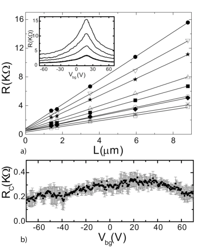
The inset of Fig. 1a shows measurements of
performed on devices fabricated on a bilayer graphene flake, with
different contacts separations ( ranging from to ) and fixed conductive channel width (). As it
appears from the main graph in Fig. 1a, at each fixed value
of the total device resistance scales linearly with .
The deviations from such a linear dependence are small, indicating
that the contact resistance for the different electrodes is
approximately the same. From the linear extrapolation of we
determine the intercept at as a function of . It
appears that is only weakly dependent on even in
the charge neutrality region (see Fig. 1b), in contrast to
the resistance of bilayer graphene, which exhibits a pronounced
peak.
We have also checked the scaling as a function of contact width but
fixed channel length, by comparing two devices fabricated on the
same flake. In this case is given by
, with
. In Fig. 2a-d we show the results
of this experiments for layers of different thickness, with the
light grey lines representing values obtained for as a
function of . Consistently with the previous results, also
these experiments show that is a gate independent quantity
over the full back gate range (), and that its
value () does not depend on the thickness of
graphene layer.
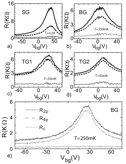
Finally, we have extracted the value of by comparing
directly two and four probe resistance measurements. In a four-probe
configuration only the resistance of the graphene channel is
measured, i.e. . From the value of
and the known device geometry we obtain the resistivity of graphene,
and use it to extract the contact resistance from resistance
measured in a two-terminal configuration . In Fig.
2e we plot and versus , together
with the extracted . Once again we find that and gate voltage independent. The fact that all these
three independent transport methods (scaling of , , and
comparison of two- and four-probe measurements) give quantitatively
consistent results confirms the validity of our analysis. Note also
that measurements performed at different temperature give the same
result, indicating that contact resistance is temperature
independent (or only very weakly temperature dependent) up to room
temperature.
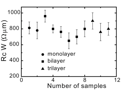
A remarkable result of our measurements emerges when comparing the
estimated value of for each different few layer graphene
device (see Fig. 3). Even though graphene-based materials
of different thickness correspond to truly different electronic
systems, with unique and characteristic low-energy electronic
properties, the value of that we have obtained from all our
measurements is independent of the number of layers: at least up to
3 layers . Since the low-energy
electronic properties of single-, bi-, and tri-layer are markedly
differentLatil , the independence of from layer
thickness suggests that a substantial charge transfer from the metal
contact to the graphene shifts the Fermi level far from the
degeneracy point. This same argument may also explain why is
independent on , since the density of charge transferred
from the metal contact can easily be much larger than the typical
modulation induced by the back gate voltage. Indeed, it has been
predicted theoretically that a large transfer of charge should occur
between many different metals and grapheneGiovannetti . For
Ti, however, no calculations have been yet performed.
In conclusion we have conducted a systematic study in transport
experiments of the contact resistance at graphene-metal (Ti/Au)
interface, using single, double and triple layer graphene. Employing
three independent methods we have established that is , independent of back gate voltage, of
temperature and of layer thickness. A significant charge transfer at
the graphene-metal interface, which shifts the Fermi level of the
few-layer graphene far away from degeneracy point, is the likely
explanation for this unexpected result.
We acknowledge financial support from FOM (AFM and SR) and the Japan
Society for the Promotion of Science, grant P07372 (MFC). M.Y.
acknowledge financial support from the Grant-in-Aid for Young
Scientists A (No. 20684011) and ERATO-JST (No. 080300000477). S.T.
acknowledges financial support from the Grant-in-Aid for Scientific
Research S (No.19104007), B (No. 18340081), JST-CREST, and Special
Coordination Funds for Promoting Science and Technology.
References
- (1) K. S. Novoselov, A. K. Geim, S. V. Morozov, D. Jiang, Y. Zhang, S. V. Dubonos, I. V. Grigorieva, and A. A. Firsov, Science 306, 666 (2004); K. S. Novoselov, A. K. Geim, S. V. Morozov, D. Jiang, M. I. Katsnelson, I. V. Grigorieva, S. V. Dubonos, and A. A. Firsov, Nature 438, 197 (2005); Y. Zhang, Y. Tan, H. L. Stormer, and P. Kim, Nature 438, 201 (2005).
- (2) A. K. Geim and K. S. Novoselov, Nature Mater. 6, 183 (2007).
- (3) M. I. Katsnelson, K. S. Novoselov, and A. K. Geim, Nature Physics 2, 620 (2006).
- (4) E. McCann, Phys. Rev. B 74, 161403 (2006).
- (5) T. Ohta, A. Bostwick, T. Seyller, K. Horn, and E. Rotenberg, Science 313, 951 (2006).
- (6) E. V. Castro, K. S. Novoselov, S. V. Morozov, N. M. R. Peres, J. M. B. Lopes dos Santos, Johan Nilsson, F. Guinea, A. K. Geim, and A. H. Castro Neto, Phys. Rev. Lett. 99 216802 (2007).
- (7) J. B. Oostinga, H. B. Heersche, X. Liu, A. F. Morpurgo, and L. M. K. Vandersypen, Nature Mater. 7, 151 (2008).
- (8) K.I. Bolotin, K.J. Sike, Z. Jian, G. Fundenberg, J. Hone, P. Kim and H.L. Stormer Solid State Commun. 146, 351-355 (2008).
- (9) P. Blake, R. Yang, S. V. Morozov, F. Schedin, L. A. Ponomarenko, A. A. Zhukov, I. V. Grigorieva, K. S. Novoselov, A. K. Geim, arxiv:0811.1459.
- (10) E. J. H. Lee, K. Balasubramanian, R. T. Weitz, M. Burghard, and K. Kern, Nature Nanotechnology 3, 486 (2008).
- (11) B. Huard, N. Stander, J. A. Sulpizio, and D. Goldhaber Gordon, Phys. Rev. B 78, 121402(R) (2008).
- (12) G. Giovannetti, P. A. Khomyakov, G. Brocks, V. M. Karpan, J. van den Brink, and P. J. Kelly, Phys. Rev. Lett. 101, 026803 (2008).
- (13) S. Malola, H. Hakkinen, and P. Koskinen, arxiv:0811.1459.
- (14) J. Cayssol, B. Huard, and D. Goldhaber-Gordon, Preprint at ¡http://arxiv.org/abs/0810.4568¿ (2008).
- (15) H.H. Heersche, P. Jarillo-Herrero, J.B. Oostinga, L.M.K. Vandersypen, and A.F. Morpurgo, Nature 446, 56-59 (2007).
- (16) P. Blake, K. S. Novoselov, A. H. Castro Neto, D. Jiang, R. Yang, T. J. Booth, A. K. Geim, E. W. Hill, Appl. Phys. Lett. 91, 063124 (2007).
- (17) D. S. L. Abergel, A. Russell, and V. I. Falko, Appl. Phys. Lett. 91, 063125 (2007).
- (18) Z. H. Ni, H. M. Wang, J. Kasim, H. M. Fan, T. Yu, Y. H. Wu, Y. P. Feng, and Z. X. Shen, Nano Letters 7, 2758-2763 (2007).
- (19) R. Golizadeh-Mojarad, and S. Datta, arxiv:0710.2727.
- (20) S. Latil, L. Henrard, Phys. Rev. Lett. 97, 036803 (2006); B. Partoens, F.M. Peeters, Phys. Rev. B 74, 075404 (2006).