Device Model for Graphene Bilayer Field-Effect Transistor
Abstract
We present an analytical device model for a graphene bilayer field-effect transistor (GBL-FET) with a graphene bilayer as a channel, and with back and top gates. The model accounts for the dependences of the electron and hole Fermi energies as well as energy gap in different sections of the channel on the bias back-gate and top-gate voltages. Using this model, we calculate the dc and ac source-drain currents and the transconductance of GBL-FETs with both ballistic and collision dominated electron transport as functions of structural parameters, the bias back-gate and top-gate voltages, and the signal frequency. It is shown that there are two threshold voltages, and , so that the dc current versus the top-gate voltage relation markedly changes depending on whether the section of the channel beneath the top gate (gated section) is filled with electrons, depleted, or filled with holes. The electron scattering leads to a decrease in the dc and ac currents and transconductances, whereas it weakly affects the threshold frequency. As demonstrated, the transient recharging of the gated section by holes can pronouncedly influence the ac transconductance resulting in its nonmonotonic frequency dependence with a maximum at fairly high frequencies.
pacs:
73.50.Pz, 73.63.-b, 81.05.UwI Introduction
The features of the electron and hole energy spectra in graphene provide the exceptional properties of graphene-based heterostructures and devices 1 ; 2 ; 3 ; 4 ; 5 ; 6 .
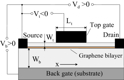
However, due to the gapless energy spectrum, the interband tunneling 7 can substantially deteriorate the performance of graphene field-effect transistors (G-FETs) with realistic device structures 8 ; 9 ; 10 ; 11 . To avoid drawbacks of the characteristics of G-FETs based on graphene monolayer with zero energy gap, the patterned graphene (with an array of graphene nanoribbons) and the graphene bilayers can be used in graphene nanoribbon FETs (GNR-FETs) and in graphene bilayer FETs (GBL-FETs), respectively. The source-drain current in GNR-FETs and GBL-FETs, as in the standard FETs, depends on the gate voltages. The positively biased back gate provides the formation of the electron channels, whereas the negative bias voltage between the top gate and the channels results in forming a potential barrier for electrons which controls the current. By properly choosing the width of the nanoribbons, one can fabricate graphene structures with a relatively wide band gap 12 (see also Refs. 13 ; 14 ; 15 ; 16 ) Recently, the device dc and ac characteristics of GNR-FETs were assessed using both numerical 14 and analytical 17 ; 18 ; 19 models. The effect of the transverse electric field (to the GBL plane) on the energy spectrum of GBLs 20 ; 21 ; 22 can also be used to manipulate and optimize the GBL-FET characteristics. A significant feature of GBL-FETs is that under the effect of the transverse electric field not only the density of the two-dimensional electron gas in the GBL varies, but the energy gap between the GBL valence and conduction bands appears. This effect can markedly influence the GBL-FET characteristics. The structure of a GBL-FET is shown in Fig. 1. In this paper, we present a simple analytical device model for a GBL-FET, obtain the device dc and ac characteristics, and compare these characteristics with those of GNR-FETs.
The paper organized as follows. In Sec. II, we consider the GBL-FET band diagrams at different bias voltages and estimate the energy gaps and the Fermi energy in different sections of the device. Section III deals with the Boltzmann kinetic equation which governs the electron transport at dc and ac voltages and the solutions of this equation. The cases of the ballistic and collision dominated electron transport are considered. In Sec. IV and Sec. V, the dc transconductance and the ac frequency-dependent transconductance are calculated using the results of Sec. III. Section VI deals with the demonstration and analysis of the main obtained results, numerical estimates, and comparison of the GBL-FET properties with those of GNR-FETs. In Sec. VII, we draw the main conclusions. In Appendix, some intermediate calculations related to the dynamic recharging of the gated section by holes due to the interband tunneling are singled out.
II GBL-FET Energy band diagrams
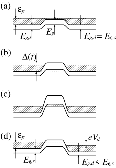
We assume that the bias back-gate voltage , while the bias top-gate voltage . The electric potential of the channel at the source and drain contacts are and , respectively, where is the bias drain voltage. The former results in the formation of a 2DEG in the GBL. The distribution of the electron density along the GBL is generally nonuniform due to the negatively biased top gate forming the barrier region beneath this gate. Simultaneously, the energy gap is also a function of the coordinate (its axis is directed in the GBL plane from the source contact to the drain contact) being different in the source, top-gate, and drain sections of the channel (see Fig. 2). Since the net top-gate voltage apart from the bias component comprises the ac signal component , the height of the barrier for electrons entering the section of the channel under the top gate (gated section) from the source side can be presented as
| (1) |
Depending on the Fermi energy in the extreme sections of the channel, in particular, on its value, , in the source section and on the height of the barrier in this section , there are three situations. The pertinent the GBL-FET energy band diagrams are demonstrated in Fig. 2. The spatial distributions of electrons and holes in the GBL channel are different depending on the relationship between the top-gate voltage and two threshold voltages, and . These threshold voltages are determined in the following.
When , the top of the conduction band in the gated section is below the Fermi level (Fig. 2a). In this case, an n+-n-n+ structure is formed in the GBL channel. At , the Fermi level is between the top of the conduction band and the bottom of the valence band in this section (Fig. 2b). This top-gate voltage range corresponds to the formation of an n+-i-n+ structure. If , both band edges are above the Fermi level (Fig. 2c), so that n+-p and p-n+ junctions are formed beneath the edges of the top gate. In the first and third ranges of the top gate voltage (“a” and “b” ranges), the electron and hole populations of the gated section are essential. In the second range (range “b”), the gated section is depleted. In the voltage range “a”, the source-drain current is associated with a hydrodynamical electron flow (due to effective electron-electron scattering) in the gated section. In this case, the source-drain current and GBL-FET characteristics are determined by the conductivity of the gated section, which, in turn, is determined by the electron density and scattering mechanisms including the electron-electron scattering mechanism, and by the self-consistent electric field directed in the channel plane. In such a situation, different hydrodynamical models of the electron transport (including the drift-diffusion model) can be applied (see, for instance, Refs. 23 ; 24 ; 25 ; 26 ; 27 ).
If , considering the potential distribution in the direction perpendicular to the GBL plane invoking the gradual channel approximation 28 ; 29 and assuming for simplicity that the thicknesses of the gate layers separating the channel and the pertinent gates, and , are equal to each other , we obtain
| (2) |
where is the electron charge. In the voltage range in question, the electron system in the gated section is not degenerate. This voltage range as well as the range correspond to the GBL-FET “off-state”. Similar formulas take place for the barrier height from the drain side (with the replacement of by ),
In the cases when or ,
| (3) |
Here are the electron and hole densities in the gated section and is the dielectric constant of the gate layers. In the most interesting case when the electron densities in the source and drain sections are sufficiently large, so that the electron systems in these sections are degenerate. Considering this, the height of the barrier is given by
| (4) |
| (5) |
when and , respectively. Here is the Bohr radius, is the effective spacing between the graphene layers in the GBL which accounts for the screening of the electric field between these layers 20 ; 21 . This quantity is smaller than the real spacing between the graphene layers in the GBL nm. The Bohr radius and parametes can be rather different in different materials of the gate layers. In the cases of Si02 and Hf02 (with 30 ; 31 ) gate gate layers, nm and nm, respectively. In deriving Eqs. (4) and (5), we have taken into account that in real GBL-FETs, .
The Fermi energy in the source section is given by
| (6) |
where is the Boltzmann constant and is the temperature, so that at sufficiently large back gate voltages,
| (7) |
Here we have considered that the electron density in the source section (the electron density in the drain section of the channel is approximately equal to ). Comparing Eqs. (2), (4), and (5), one can see that the height of the barrier increases with increasing absolute value of the top-gate voltage rather slow in the voltage ranges “a” and “c” in contrast to its steep increase in the voltage range “b”.
Since the energy gaps in GBLs , , and depend on the local transverse electric field 20 ; 21 ; 22 , so that they are different in different sections of the channel depending on the bias voltages:
| (8) |
One can see that at and , one obtains .
The threshold voltages and are determined by the conditions and ,respectively. The latter implies that the Fermi energy of holes in the gated section . As a result, the threshold voltages are given by
| (9) |
Since one can assume that , the threshold voltages are close to each other: with . The values of the energy gap in the gated section at the threshold top gate voltages are given by
| (10) |
In the following we restrict our consideration by the situations when the height of the barrier for electrons in the gated section is sufficiently large (so that ), which corresponds to the band diagrams shown in Figs. 2(b) and 2(c).
III Boltzmann kinetic equation and its solutions
The quasi-classical Boltzmann kinetic equation governing the electron distribution function in the section of the channel covered by the top gate (gated section) can be presented as
| (11) |
Here, taking into account that the electron (and hole) dispersion relation at the energies close to the bottom of the conduction band is virtually parabolic with the effective mass ( g), for the energy of electron with momentum we put , , where (the -axis and the -axis are directed in the GBL plane) and is the probability of the electron scattering on disorder and acoustic phonons with the variation of the electron momentum by quantity .
The density of the electron (thermionic) current, , in the gated section of the channel (per unit length in the -direction) can be calculated using the following formula:
| (12) |
where is the reduced Planck constant.
Disregarding the electron-electron collisions in the gated section of the channel (due a low electron density in this section in contrast to the source and drain sections where the electron-electron collisions are essential), we consider two limiting cases: ballistic transport of electrons across the gated section and strongly collisional electron transport.
III.1 Ballistic electron transport
If , where and are the amplitude and frequency of the ac signal, then the electron distribution function can be searched as and . Assuming that and solving Eq. (11) with the boundary conditions
| (13) |
where is the top gate length, we obtain
| (14) |
| (15) |
Here, is the unity step function. The first boundary condition given by Eq. (14) corresponds to quasi-equilibrium electron distribution in the source section of the channel and the injection of electrons with the kinetic energy exceeding the barrier height from the source section to the gated section (at ). The injection of electrons from the drain source to the gated section (at ) is negleted due to ; this inequality leads to rather high barrier near the drain edge of the gated section. The presence of the unity step fuction in Eqs. (16) and (17) reflects the fact that there are no electrons propagating backwards due to the absence of the electron scattering in the gated section.
Using Eqs. (12), (14), and (15), we arrive at the following formulas for the dc and ac components, and , of the current at the drain edge of the gated section (i.e., at )
| (16) |
| (17) |
Here
where is the effective ballistic transit time across the gated section of electrons with the thermal velocity and and are Frenel’s cosine and sine functions. At ,
At , tends to unity.
III.2 Collisional electron transport
In the case of strongly collisional electron transport, the distribution function in the gated section is close to isotropic and it can be searched in the form
| (18) |
Here is the symmetrical part of the electron distribution function (which is generally not the equilibrium function). The second term in Eq. (18) presents the asymmetric part of the distribution function with . Similar approach was used for the calculation of characteristics of heterojunction bipolar transistors 32 (see also Refs. 19 ; 33 ). As a result, after the averaging of Eq. (11) over the angle , one can arrive at the following coupled equations:
| (19) |
Here in the case of , which corresponds to the scattering of electrons on short-range defects, . Equations (19) are reduced to the following equation for function :
| (20) |
In the most interesting case when , the boundary conditions for Eq. (20) at and , can be adopted in the following form:
| (21) |
The boundary condition under consideration imply that at there is the electron injection from the source section of the channel, whereas at an effective extraction of the electrons into the drain section occurs due to a strong pulling dc electric field. Due to a strong electron scattering a significant portion of the injected electrons returns back to the source section.
Setting as above and, hence, and , we obtain
| (22) |
| (23) |
and arrive at
| (24) |
| (25) |
where . Considering Eqs. (19), (24), and (25) , we obtain
| (26) |
| (27) |
After that, using Eqs. (12), (26), and (27), we arrive at the following formulas for and (at ):
| (28) |
| (29) |
Here
According to Eq. (28), . One needs to stress that the collisional case under consideration corresponds actually to . In the frequency range , . At , one obtains
IV GBL-FET dc transconductance
Equations (16) and (28) provide the dependences of the source-drain dc current as a function of the device structural parameters, temperature, and back- and top-gate voltages for GBL-FETs with ballistic and collisional electron transport, respectively (in the limit ). Using Eq. (16), one can find the dc transconductance of a GBL-FET with the ballistic electron transport:
| (30) |
when , and
| (31) |
when . Here
| (32) |
Similarly, using Eq. (28), we obtain the following formulas for the GBL-FET transconductance in the case of collisional electron transport:
| (33) |
when and
| (34) |
when .
As follows from the comparison of Eq. (30) with Eq. (31) and Eq. (33) with Eq. (34), the GBL-FET dc transconductance in the top gate voltage range (in the range “b”) might be much larger than that when (in the range “c”) since . This is due to relatively slow increase in with increasing when the hole density in the gated section becomes essential.
The voltage dependences of the dc transconductance can be obtained using Eqs. (30), (31), (33), and (34) and invoking Eqs. (2), (4), and (6). In particular, in a rather narrow voltage range , one obtains
| (35) |
At sufficiently large absolute values of the top-gate voltage when , the transconductance vs voltage dependence is given by
| (36) |
V GBL-FET ac transconductance
According to the Shockley-Ramo theorem 34 ; 35 , the source-drain ac current is equal to the ac current induced in the highly conducting quasi-neutral portion of the drain section of the channel and in the drain contact by the electrons injected from the gated section. This current is determined by the injected ac current given by Eq. (16) or Eq. (28) as well as the electron transit-time effects in the depleted portion of the drain section. However, if , where the is the electron transit time in depleted region in question, the induced ac current is very close to the injected ac current 19 ; 36 ; 37 . Since, at moderate drain voltages, the length of depleted portion of the drain section can usually be shorter than the top gate length , in the most practical range of the signal frequencies , one can assume that and, hence, . Considering this and using Eqs. (17) and (28), the GBL-FET ac transconductance at different electron transport conditions can be presented as
| (37) |
| (38) |
respectively.
In the range of gate voltages (range “b”), Eq. (2) yields
| (39) |
In this case, Eqs. (37) and (38) result in
| (40) |
| (41) |
As follows from Eqs. (40) and (41), the characteristic frequencies of the ac transconductance roll-off are and in the case of the ballistic and collisional electron transport, respectively, i.e., the inverse times of the ballistic and diffusive transit across the gated section of the channel. Indeed, the quantity can be presented as , where is the electron diffusion coefficient.

The situation becomes more complex in the range of the top gate bias voltages (range “c”). As follows from Eq. (4) in this voltage range, the quantity is determined not only by the ac voltage but also by the ac component of the hole density in the gated section . Moreover, at sufficiently high signal frequencies, the hole system in the gated section can not manage to follow the variation of the ac voltage. Taking into account the dynamic response of the hole system (see Appendix A), instead of Eq. (39) one can obtain
| (42) |
Here (see Appendix A)
| (43) |
where is the time of the gated section recharging associated with changing of the hole density due to the tunneling or/and generation-recombination processes. Generally, depends on the top gate length .
Accounting for Eq. (42), we arrive at the following formulas for the GBL-FET ac transconductance when :
| (44) |
| (45) |
If , one obtains and the ac transconductances in both “b” and “c” ranges of the top gate voltage are close to each other (compare Eqs. (40) and (41) with Eqs. (42) and (44)). However, at low signal frequencies ( ), the ac transconductance given by Eq. (44) or (45) for the voltage range “c” are markedly smaller than those given by Eqs. (40) or (41) valid in the voltage range “b”.
VI Analysis of the results and discussion
Comparing and given by Eqs. (30) and (35), we obtain . This implies that the above ratio markedly decreases with increasing collision frequency (with decreasing electron mobility) and the top gate length, i.e., with the departure from the ballistic transport.
As shown above, the dc current steeply drops in a narrow top-gate voltage range . Inded, the ratio . Setting nm, K, and V, we find . The estimate of the dc current at (which might be interesting for the GBL-FET applications in digital large scale circuits) with nm, K, and V yields A/cm. At K and V, one obtains A/cm. In the case of a GBL-FET with the width m, the latter corresponds to the characteristic value of the “off- current” pA. Similar values can be obtained at K when V.
As follows from Eq. (35), the GBL dc transconductance in the range of the top gate voltages is particularly large when . This is due to a sharp voltage- sensitivity of the dc current and its relatively high values at such voltages. Indeed, using Eq. (28) at K and , we obtain mS/mm. In GBL-FETs with , the dc transconductance can be even larger.
The pre-exponential factor in the right-hand side of Eq. (36) is proportional to a small parameter . The argument of the exponential function in this equation comprises small parameters and . This implies that the dc transconductance in the voltage range described by Eq. (36) is relatively small and is a faily weak function of the top-gate voltage. As follows from Eqs. (35) and (36), the ratio of the dc transconductance at to that at is equal approximately to the following small value: ; it is smaller then the ratio of the dc currents by parameter .
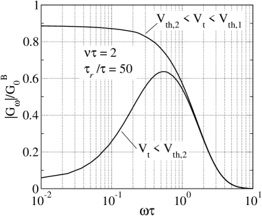
Figure 3 shows the ac transconductance normalized by the dc transconductance at the ballistic transport as a function of the normalized signal frequency calculated for GBL-FETs with both ballistic and collisional electron transport. It is assumed that the top gate voltage is in the range . The inset in Fig. 3 shows the dependence of the normalized threshold frequency on . The threshold frequency is defined as that at which . One can see that pronouncedly decreases with increasing collision frequency. However, as seen from the inset in Fig. 3, the decrease in with increasing is markedly slower: the ratio of at and at (i.e., three times larger) is approximately equal to 1.42. Setting nm and K, for the threshold frequency at the ballistic transport we obtain THz. To realize the near ballistic regime of the electron transport () in GBL-FETs with such gate lengths, the electron mobility cm2/Vs is required. The possibility of the latter mobilities at room temperatures was discussed recently (see, for instance, Ref. 6 ). At a shorter top gate, nm, one obtains THz. In the case of a GBL-FET with relatively long top gate and moderate mobility ( nm and cm2/Vs) when the effect of scattering is strong ( s-1 and ), we obtain GHz.
In Fig. 4, the similar dependences calculated for a GBL-FET with collisional electron transport at and at are demonstrated. Since in the latter top-gate voltage range the electron scattering on holes accumulated in the gated section can be strong, so that the realization of the ballistic transport at such top-gate voltages might be problematic, only the dependences corresponding to the collisional electron transport are shown. As follows from Eqs. (44) and (45) and seen from Fig. 4, the ac transconductance at the top gate voltages is fairly small at low frequencies being close to the dc transconductance (due to a smallness of parameter ), whereas it becomes much larger in the intermediate frequency range (or ). This is due to the effect of holes in the gated section. Owing to this effect, the low frequency noises can be effectively suppressed.
Using the above results for GBL-FETs and those obtained previously 19 for GNR-FETs, one can compare the GBL and GNR characteristics. In particular, considering the expressions for found for GBL-FETs and GNR-FETs, we obtain . For the case of collisional transport, one obtains . As a result, the GBL-FET and GNR-FET dc transconductances are close to each other. The ratio of the GBL-FET and GNR-FET ac transconductances at high signal frequencies is , i.e., the GBL-FET ac transconductance falls more steeply with increasing than the GNR-FET ac transconductance.
The GBL-FET dc and ac characteristics obtained are valid if the interband tunneling source-drain current through the and junctions beneath the edges of the top gate are small in comparison with the thermionic current created by the electrons overcoming the potential barrier in the gated section. Such a tunneling current can be essential in the voltage range ”c” () depending on the energy gap near the top gates and the length of the and junctions in question. This implies that there is a limitation when the top-gate voltage is not too high in comparison with the threshold voltage (i.e., when ), so that the calculated characteristics correspond to the most interesting voltage range where the ac transconductance can be rather large.
VII Conclusions
We have presented an analytical device model for a GBL-FET.
Using this model, we have
calculated the GBL-FET dc and ac characteristics and shown that:
(1) The dependence of the dc current on the top gate voltage
is characterized by the existence of three voltage ranges,
corresponding to (a) the population of the gated section by electrons,
(b) the depletion of this section, and (c)
its essential filling with holes,
and
determined by the top-gate threshold voltages and .
(2) The ac current is most sensitive to the top-gate voltage
and the dc and ac transconductances are large when
.
(3) The electron scattering in the gated section results in a marked
reduction in the dc and ac transconductances. However,
the threshold frequency corresponding to
decreases with increasing collision frequency relatively smoothly.
(4) The transient recharging of the gated section by holes (at )
leads to a nonmonotonic frequency dependence of the ac transconductance
with a pronounced maxima in the range of fairly high frequencies.
This effect might be used for the optimization of GBL-FETs with
reduced sensitivity to low frequency noises.
(5) The fabrication of GBLs with high electron mobility
at elevated temperatures opens up the prospects
of realization of terahertz GBL-FETs with ballistic electron transport
operating at room temperatures and
surpassing FETs based on A3B5 compounds.
Acknowledgments
The authors are grateful to Professor S. Brazovskii (University Paris-Sud) and Professor E. Sano (Hokkaido University) for fruitful discussions and valuable information. The work was supported by the Japan Science and Technology Agency, CREST, Japan. One of the authors (N.K.) acknowledges the support by the INTAS grant 7972, and by the ANR program in France (the project BLAN07-3-192276).
Appendix A. Dynamic response of the hole system in the gated section
At sufficiently large values , the gated section is essentially populated with the holes. As follows from eq. (4),
| (A1) |
The ac component of the hole density obeys the continuity equation which can be presented in the following form:
| (A2) |
Here is the variation of the generation pf holes in the gated section (associated, say, with the generation of holes by the thermal radiation 38 ) and and are the interband tunneling ac currents near the source and drain edges of the top gate, respectively. For normal operation of GBL-FETs, these tunneling current should relatively small. This is achieved in GNL-FETs by proper choice of the energy gap in the different sections of the channel (, , and which should be not too small. The terms in thr right-hand side of eq. (A2) can be presented as
| (A3) |
| (A4) |
Here , , where is the characteristic time of the generation-recombination processes in the gated section, is the tunneling resistance of the p-n junctions induced by the negative top gate voltage near the edges of the top gate: . From eqs. (A1) - (A4), taking into account the limit (see eqs. (5) and (30)), we find
| (A5) |
where is the time of the gated section recharging by the tunneling currents, is the tunneling resistance of the p-n junctions induced by the negative top gate voltage near the edges of the top gate, the quantity is the characteristic time of the gated section recharging by holes, and is the capacitance of the gated section. At , eq. (A5) leads to
| (A6) |
where
i.e., coincides with the value given by eq. (28). When , eq. (A5) yields
| (A7) |
References
- (1) C. Berger, Z. Song, T. Li, X. Li, A.Y. Ogbazhi, R. Feng, Z. Dai, A. N. Marchenkov, E. H. Conrad, P. N. First, and W. A. de Heer, J. Phys. Chem. 108, 19912 (2004).
- (2) K. S. Novoselov, A. K. Geim, S. V. Morozov, D. Jiang, M. I. Katsnelson, I. V. Grigorieva, S. V. Dubonos, and A. A. Firsov, Nature 438, 197 (2005).
- (3) B. Obradovic, R. Kotlyar, F. Heinz, P. Matagne, T. Rakshit, M. D. Giles, M. A. Stettler, and D. E. Nikonov, Appl. Phys. Lett. 88, 142102 (2006).
- (4) J. Hass, R. Feng, T. Li, X. Li, Z. Zong, W. A. de Heer, P. N. First, E. H. Conrad, C. A. Jeffrey, and C. Berger: Appl. Phys. Lett. 89, 143106 (2006).
- (5) A. K. Geim and K. S. Novoselov, Nat. Mater. 6, 183 (2007).
- (6) S. V.Morozov, K. S. Novoselov, M. I. Katsnelson, F. Schedin, D. C. Elias, J. A. Jaszczak, and A. K. Geim, Phys. Rev. Lett. 100, 016602 (2008)
- (7) V. V. Cheianov and V. I. Fal’ko, Phys. Rev. B 74, 041403 (2006).
- (8) B. Huard, J. A. Sulpizio, N. Stander, K. Todd, B. Yang, and D. Goldhaber-Gordon, Phys. Rev. Lett. 98, 236803 (2007).
- (9) M. C. Lemme, T. J. Echtermeyer, M. Baus, and H. Kurz, IEEE Electron Device Lett. 28, 282 (2007).
- (10) V. Ryzhii, M. Ryzhii, and T. Otsuji, Appl. Phys. Express, 1, 013001 (2008),
- (11) V. Ryzhii, M. Ryzhii, and T. Otsuji, Phys. Stat. Sol. (a) 205, 1527 (2008).
- (12) Z. Chen, Y.-M. Lin, M. J. Rooks, and P. Avouris, Physica E 40 228(2007).
- (13) K. Wakabayshi, Y. Takane, and M. Sigrist, Phys. Rev. Lett. 99, 036601 (2007).
- (14) Y. Quyang, Y. Yoon, J. K. Fodor, J. Guo, Appl. Phys. Lett. 89, 203107 (2006).
- (15) G. Liang, N. Neophytou, D. E. Nikonov, and M. S. Lundstrom, IEEE Tran. Electron Devices 54, 677 (2007).
- (16) G. Fiori and G. Iannaccone, IEEE Electron Device Lett. 28, 760 (2007).
- (17) V. Ryzhii, M. Ryzhii, A. Satou, and T. Otsuji, J. Appl. Phys. 103, 094510 (2008).
- (18) V. Ryzhii, V. Mitin, M. Ryzhii, N. Ryabova, and T. Otsuji, Appl. Phys. Express. 1, 063002 (2008).
- (19) M. Ryzhii, A. Satou, V. Ryzhii, and T. Otsuji, J. Appl. Phys. 104, 114505 (2008).
- (20) T. Ohta, A. Bostwick, T. Seyel, K. Horn, E. Rotenberg, Science 313,951 (2006).
- (21) E. McCann, Phys. Rev. B 74, 161403 (2006).
- (22) E. V. Castro, K. S. Novoselov, S. V.Morozov, N. M. R. Peres, J. M. L. dos Santos, J. Nilsson, F. Guinea, A. K. Geim, and A. H. Castro Neto, Phys. Rev. Lett. 99, 216802 (2007)
- (23) L. A. Falkovski Phys. Rev. B 75, 033409 (2007).
- (24) F. T. Vasko and V. Ryzhii, Phys. Rev. B 76, 233404 (2007).
- (25) V. Vyurkov and V. Ryzhii, JETP Lett. 88, No.5 (2008).
- (26) M. G. Ancona, 2008 Int. Conf. Semicond. Processes and Devices (SISPAD 2008), Sept. 9-11, 2008, Hakone, Japan, p. 169.
- (27) V. Vyurkov, I. Seminikhin, M.Ryzhii, T. Otsuji, and V. Ryzhii, Techn. Digest, Int. Symp. on Graphene Devices: Technology, Physics, and Modeling (ISGD2008), Nov. 17-19, 2008, Aizu-Wakamatsu, Japan,, p .32.
- (28) M. Shur, Physics of Semiconductor Devices (Prentice Hall, New Jersey, 1990).
- (29) S. M. Sze, Physics of Semiconductor Devices (Wiley, New York, 1981).
- (30) E. P. Gusev, C. Carbal Jr., M. Copel, C. D’Emic, and M. Gribelenuk, Microelectron. Eng. 63, 145 (2003).
- (31) Y. Xuan, Y. Q. Wu, T. Shen, M. Qi, M. A. Capano, J. A. Cooper, and P. D. Ye, App. Phys. Lett. 92, 013101 (2008).
- (32) V. I. Ryzhii, A. A. Zakharova, and S. N. Panasov, Sov. Phys. Semicond. 19, 298 (1985).
- (33) E. Gnani, A. Gnudi, S. Reggiani, and G. Baccarani, IEEE Trans. on Electron Devices, 55, 2918 (2008)
- (34) W. Shockley, J. Appl. Phys. 9, 635 (1938)
- (35) S. Ramo, Proc. IRE 27, 584 (1939).
- (36) V. Ryzhii and G. Khrenov, IEEE Trans. Electron Devices 42, 166 (1995).
- (37) V. Ryzhii, A. Satou, M. Ryzhii, T. Otsuji, and M. S. Shur, J. Phys. Cond. Mat. 20, 384207 (2008)..
- (38) F. T. Vasko and V. Ryzhii, Phys. Rev. B 77, 195433 (2008).