Frequency doubling and memory effects in the Spin Hall Effect
Abstract
We predict that when an alternating voltage is applied to a semiconducting system with inhomogeneous electron density in the direction perpendicular to main current flow, the spin Hall effect results in a transverse voltage containing a double-frequency component. We also demonstrate that there is a phase shift between applied and transverse voltage oscillations, related to the general memristive behavior of semiconductor spintronic systems. A different method to achieve frequency doubling based on the inverse spin Hall effect is also discussed.
pacs:
72.25.Dc, 71.70.EjIn optics, frequency doubling (also called second harmonic generation) is obtained from nonlinear processes, in which the frequency of photons interacting with a nonlinear material is doubled. This phenomenon was first observed in 1961 SG1 and has found numerous applications in diverse areas of science and engineering SG2 . Physically, the fundamental (pump) wave propagating through a crystal with nonlinearity (due to the lack of inversion symmetry) generates a nonlinear polarization which oscillates with twice the fundamental frequency radiating an electromagnetic field with this doubled frequency. In electronics, frequency doubling is a fundamental operation for both analog and digital systems, which is however achieved via complex circuits made of both passive and active circuit elements freqd .
As we demonstrate in this Letter, the possibility of generating frequency doubling need not be limited to optical processes in crystals, or require complex circuits. In fact, we show it can be realized via a completely different physical mechanism using the spin Hall effect spinHall . Our idea is to use a material with inhomogeneous doping in the direction perpendicular to the main current flow. As it was recently shown vprobe , a dc voltage applied to such a system results in a transverse voltage, similar to the Hall voltage, but with a different symmetry: the sign of the transverse voltage due to the spin Hall effect does not depend on the polarity of the applied field. Therefore, when an ac voltage is applied, the transverse voltage oscillations are similar in the positive and negative half-periods of the applied voltage, which results in the frequency doubling.
Moreover, the transverse voltage oscillations show hysteretic behavior at different frequencies. This result is reminiscent of the recent experimental demonstration of memory-resistive (memristive) behavior in certain nanoscale systems memr1 ; memr2 and is consistent with our suggestion spinmemr that some semiconductor spintronic systems are intrinsically memristive systems chua76 . When a time-dependent voltage is applied to such systems, their response is delayed because the adjustment of spin polarization to changing driving field requires some time (due to spin relaxation and diffusion processes). In other words, the electron spin polarization has a short-time memory on its previous state spinmemr . A unique feature of the system investigated in this work is that effects of spin memory manifest themselves in the voltage response, while in the previous study spinmemr spin memory effects were predicted in the current. Below, we study the frequency doubling and manifestation of spin memristive effects both analytically and numerically. This work reveals fundamental aspects of the spin Hall effect that have not been explored yet, as well as its possible use in electronic circuits.
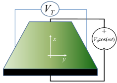
Fig. 1 shows a possible experimental setup which can be used to observe frequency doubling by using the spin Hall effect. An alternating voltage of frequency and amplitude is applied along a sample of semiconductor material (we call this direction). The electron density in the semiconductor is inhomogeneous in the direction () perpendicular to main current flow. A transverse time-dependent voltage then develops between the sample boundaries and , where is the sample width. According to our previous calculations vprobe and recent experimental results miah , it is expected that the transverse voltage oscillation amplitude is a non-linear function of .
To study this system, we employ a self-consistent two-component drift-diffusion model flatte ; PDV which is appropriate for the physics of this problem. The inhomogeneous charge density profile is defined via an assigned positive background density profile (such as the one shown in Fig. 1), which can be obtained in different ways including inhomogeneous doping, variation of sample height or gate-induced variation of electron density. Assuming homogeneous charge and current densities in the direction and homogeneous -component of the electric field in both and directions, the set of equations to be solved is
| (1) |
| (2) |
and
| (3) |
where is the electron charge, is the density of spin-up (spin-down) electrons, is the current density, is the spin relaxation time, is the spin-up (spin-down) conductivity, is the mobility, is the diffusion coefficient, is the permittivity of the bulk, and is the parameter describing deflection of spin-up (+) and spin-down (-) electrons. The current in -direction is coupled to the homogeneous electric field in the same direction as . The last term in Eq. (2) is responsible for the spin Hall effect.
Equation (1) is the continuity relation that takes into account spin relaxation and Eq. (3) is the Poisson equation. Equation (2) is the expression for the current in direction which includes drift, diffusion and spin Hall effect components. We assume here for simplicity that , , and are equal for spin-up and spin-down electrons. prec In our model, as it follows from Eq. (2), the spin Hall correction to spin-up (spin-down) current (the last term in Eq. 2) is simply proportional to the local spin-up (spin-down) density. All information about the microscopic mechanisms for the spin Hall effect is therefore lumped in the parameter .
Combining equations (1) and (2) for different spin components we can get the following equations for the electron density and the spin density imbalance :
| (4) |
and
| (5) |
Analytical solution – Before solving Eqs. (3)-(5) numerically, an instructive analytical result can be obtained in the specific case of exponential doping profile , with a positive constant. At small values of , we search for a solution in the form , , . Setting , the leading terms in the above expansions can be easily obtained (see also Ref. vprobe, ): , , . Next, using Eq. (5) and neglecting the term , we obtain
| (6) |
Combining Eqs. (3), (4), and (6), integrating in and neglecting the term proportional to (this approximation neglects small-amplitude higher harmonics terms), we obtain the following equation for
| (7) |
Equation (7) already demonstrates that the driving term for involves a doubled frequency. In order to further proceed, let us consider a sample of a finite width , in which doping level variations are not dramatic. Then, in the first term in the right hand side of Eq. (7), we can write approximately , where . This approximation allows us to find
| (8) |
where , defined as , is a phase shift, and
| (9) | |||||
| (10) | |||||
| (11) |
Finally, the transverse voltage is given by
| (12) |
Equation (12) demonstrates that there are two contributions to the transverse voltage : a shift term (proportional to ) and a double-frequency phase-shifted oscillation term (proportional to ). We have found that Eq. (12) is in excellent agreement with results of our numerical calculations (given below) with the only one adjustable parameter . For a particular set of parameters used below, a perfect match between analytical and numerical calculations was obtained at .
Numerical solution – Equations (3)-(5) can be solved numerically for any reasonable form of . We choose an exponential profile for its simplicity, the possibility to realize it in practice, and for the purpose of comparison with the above analytical results. We solve these equations iteratively, starting with the electron density close to and close to zero and recalculating at each time step. prec1 At each time step, the transverse voltage is calculated as a change of the electrostatic potential across the sample.
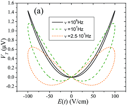
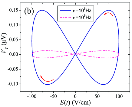
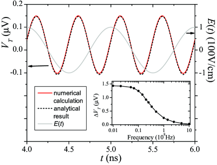
Selected results of our numerical calculations are presented in Figs. 2 and 3. In particular, Fig. 2 demonstrates that the transverse voltage oscillations are indeed of a doubled-frequency character and phase-shifted with respect to the applied voltage. Another important feature shown in Fig. 2 is the excellent agreement between our analytical and numerical results. This agreement was obtained by an appropriate choice of the parameter defined after Eq. (7). We observed that slightly depends on and , and, once is selected, the numerical and analytical solutions are in a good agreement in a wide range of excitation voltage parameters.
Multiple signatures of spin memristive behavior are clearly seen in Figs. 2 and 3 including, constant and phase shifts in depicted in Fig. 2, frequency dependence of the transverse voltage oscillation amplitude shown in the inset of Fig. 2, and hysteresis behavior plotted in Fig. 3. All these features have a common origin: the adjustment of electron spin polarization to changing voltage takes some time. In particular, at low frequencies, we observe a small hysteresis in Fig. 3(a) because when the applied electric field is changed slowly (on equilibration time scale), at each moment of time the instantaneous is very close to its equilibrium value irrespective of the driving field . At high frequencies, the situation is opposite: when the applied electric field changes very fast, the electrons “experience” an average (close to zero) applied electric field, resulting in a significantly reduced transverse voltage oscillations amplitude.
We also note that at those moments of time when , the transverse voltage is very close to, but not exactly, zero. This small deviation from an ideal memristive behavior chua76 (predicting when and related to the absence of energy storage) should be a common feature of solid-state memristive systems operating at frequencies comparable to the inverse characteristic time of charge equilibration processes.
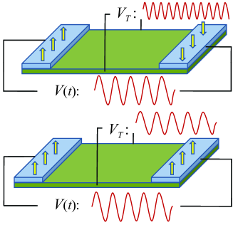
We conclude by noting that another way to realize the frequency doubling discussed in this paper can be realized by sandwiching a nonmagnetic homogeneous material between two ferromagnets (see schematic in Fig. 4). In this case one can employ the inverse spin Hall effect, in which the spin current flowing in the nonmagnetic material induces transverse charge current, and thus causes charge accumulation ishe1 ; ishe2 ; ishe3 ; ishe4 ; ISH . Since the electromotive force in the inverse spin Hall effect is ISH , where is the spin current along the sample and is the Pauli matrix, the simultaneous change of the current direction and its spin polarization, that occurs at antiparallel magnetization of ferromagnetic contacts, does not change the electromotive force polarity leading to transverse voltage oscillations with a doubled frequency. On the other hand, for parallel orientation of the spin polarization of the ferromagnetic contacts, the direction of spin current changes within each voltage cycle but not the the direction of spin polarization. This thus results in a transverse voltage with the same frequency as the longitudinal one, albeit with lower amplitude (see Fig. 4). However, since spin injection allows for much higher levels of electron spin polarization (of the order of several tens of percents) compared to the spin Hall effect (normally, less than one percent), we expect the amplitude of oscillations to be larger in the inverse spin Hall effect. An external magnetic field can also be used in such experiments as an additional control parameter.
Finally, the phenomena we predict can be easily verified experimentally. They provide additional insight on the spin Hall effect and may find application in, e.g., analog electronics requiring frequency doubling. We thus hope our work will motivate experiments in this direction.
This work has been partially funded by the NSF grant No. DMR-0802830.
References
- (1) P. A. Franken, A. E. Hill, C. W. Peters, and G. Weinreich, Phys. Rev. Lett. 7, 118 (1961).
- (2) See, e.g., N. Bloembergen, Rev. Mod. Phys. 54, 685 (1982); C. Winterfeldt, C. Spielmann, and G. Gerber, Rev. Mod. Phys. 80, 117 (2008).
- (3) K. W. Current and A. B. Current, Int. J. Electr. 45, 431 (1978).
- (4) M. I. Dyakonov and V. I. Perel, Sov. Phys. JETP Lett. 13, 467 (1971); M. I. Dyakonov and V. I. Perel, Phys. Lett. A 35, 459 (1971); J. E. Hirsch, Phys. Rev. Lett. 83 1834 (1999).
- (5) Yu. V. Pershin and M. Di Ventra, J. Phys.: Cond. Matt. 20, 025204 (2008).
- (6) D. B. Strukov, G. S. Snider, D. R. Stewart, and R. S. Williams, Nature (London) 453, 80 (2008).
- (7) J. J. Yang, M. D. Pickett, X. Li, D. A. A. Ohlberg, D. R. Stewart, and R. S. Williams, Nat. Nano. 3, 429 (2008).
- (8) Yu. V. Pershin and M. Di Ventra, Phys. Rev. B 78, 113309 (2008).
- (9) L. O. Chua and S. M. Kang, Proc. IEEE 64, 209 (1976).
- (10) M. I. Miah, Mat. Chem. and Phys. 111, 419 (2008).
- (11) Z. G. Yu and M. E. Flatté, Phys. Rev. B 66, 201202(R) (2002); W.-K. Tse, J. Fabian, I. Ẑutić and S. Das Sarma, Phys. Rev. B 72, 241303(R) (2005).
- (12) Yu. V. Pershin and M. Di Ventra, Phys. Rev. B 75, 193301 (2007).
- (13) This is a good approximation for the range of parameters considered in this work.
- (14) We have employed the Scharfetter-Gummel discretization scheme [D. L. Scharfetter and H. K. Gummel, IEEE. Trans. Electron. Devices ED-16, 64 (1969)] to solve both Eqs. (4) and (5) numerically.
- (15) A. A. Bakun, B.P. Zakharchenya, A.A. Rogachev, M.N. Tkachuk, and V.G. Fleisher, Sov. Phys. JETP Lett. 40, 1293 (1984).
- (16) H. Zhao, E. J. Loren, H. M. van Driel, and A. L. Smirl, Phys. Rev. Lett. 96, 246601 (2006).
- (17) S.O. Valenzuela and M. Tinkham, Nature 442, 176 (2006).
- (18) T. Kimura, Y. Otani, T. Sato, S. Takahashi, and S. Maekawa, Phys. Rev. Lett. 98, 156601 (2007).
- (19) K. Harii, K. Ando, K. Sasage, and E. Saitoh, Phys. Stat. Sol. (c) 4, 4437 (2007).